

Page 1
MAX1843
2.7A, 1MHz, Low-Voltage, Step-Down Regulator with
Internal Synchronous Rectification in QFN Package
________________________________________________________________ Maxim Integrated Products 1
19-1986; Rev 1; 3/02
General Description
The MAX1843 constant-off-time, pulse-width modulated
(PWM) step-down DC-DC converter is ideal for use in 5V
and 3.3V to low-voltage conversion necessary in notebook and subnotebook computers. This device features
an internal PMOS power switch and internal synchronous
rectification for high efficiency and reduced component
count. An external Schottky diode is not required. The
internal 90mΩ power switch and 70mΩ NMOS synchronous-rectifier switch easily deliver continuous load currents up to 2.7A. The MAX1843 produces a preset +2.5V,
+1.8V, or +1.5V output voltage or an adjustable output
from +1.1V to VIN. It achieves efficiencies as high as
95%.
The MAX1843 uses a unique current-mode, constant-offtime, PWM control scheme, which includes Idle Mode™
to maintain high efficiency during light-load operation.
The programmable constant-off-time architecture sets
switching frequencies up to 1MHz, allowing the user to
optimize performance trade-offs between efficiency, output switching noise, component size, and cost. The
MAX1843 features an adjustable soft-start to limit surge
currents during startup, a 100% duty-cycle mode for low
dropout operation, and a low-power shutdown mode that
disconnects the input from the output and reduces supply current below 1µA. The MAX1843 is available in a 28pin QFN package with an exposed backside pad.
Applications
5V or 3.3V to Low-Voltage Conversion
CPU I/O Ring
Chipset Supplies
Notebook and Subnotebook Computers
Features
♦ ±1% Output Accuracy
♦ Up to 1MHz Switching Frequency
♦ 95% Efficiency
♦ Internal PMOS/NMOS Switches
90mΩ/70mΩ On-Resistance at V
IN
= +4.5V
110mΩ/80mΩ On-Resistance at V
IN
= +3V
♦ Output Voltage
+2.5V, +1.8V, or +1.5V Pin Selectable
+1.1V to V
IN
Adjustable
♦ +3V to +5.5V Input Voltage Range
♦ 350µA Operating Supply Current
♦ <1µA Shutdown Supply Current
♦ Programmable Constant-Off-Time Operation
♦ Idle Mode Operation at Light Loads
♦ Thermal Shutdown
♦ Adjustable Soft-Start Inrush Current Limiting
♦ 100% Duty Cycle During Low-Dropout Operation
♦ Output Short-Circuit Protection
♦ 28-Pin QFN Package
PART TEMP RANGE PIN-PACKAGE
Ordering Information
Idle Mode is a trademark of Maxim Integrated Products.
EVALUATION KIT
AVAILABLE
MAX1843EGI -40°C to +85°C 28 QFN
MAX1843
2526
27
28 22
2324
8
9
10 11 12 13 14
15
16
17
18
19
20
21
1
2
3
4
5
6
7
REF
TOFF
FB
N.C.
N.C.
N.C.
GND
N.C.
N.C.
N.C.
LX
N.C.
LX
LX
IN
SS
COMP
IN
N.C.
LX
LX
PGND
V
CC
FBSEL
PGND
PGND
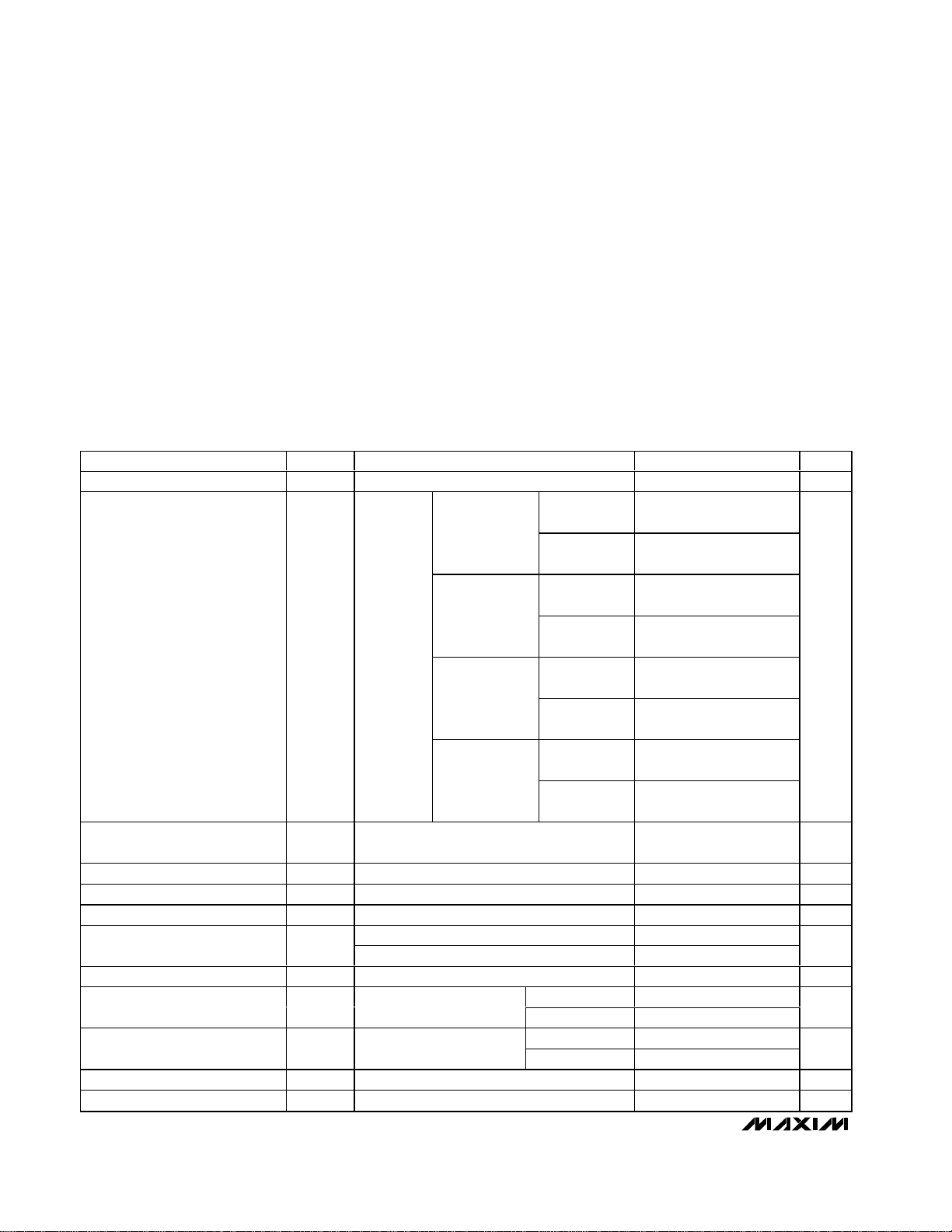
QFN
TOP VIEW
N.C.
SHDN
Pin Configuration
TOFF
COMP
V
CC
FBSEL
SHDN
IN
PGND
GND
REF
SS
LX
FB
MAX1843
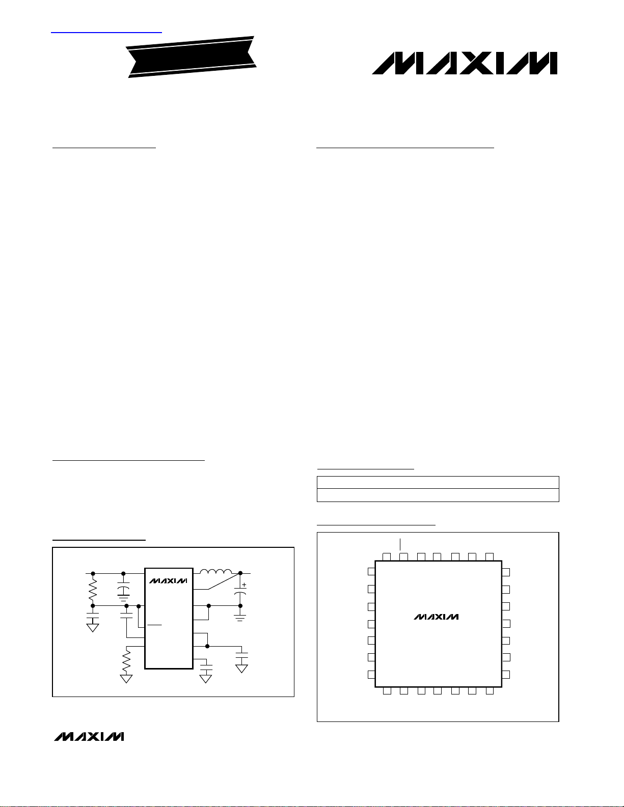
OUTPUT
+1.1V TO
V
IN
INPUT
+3V TO
+5.5V
0.01µF
1µF
2.2µF
470pF
10Ω
Typical Configuration
For pricing, delivery, and ordering information, please contact Maxim/Dallas Direct! at
1-888-629-4642, or visit Maxim’s website at www.maxim-ic.com.
查询MAX1843供应商
Page 2
MAX1843
2.7A, 1MHz, Low-Voltage, Step-Down Regulator with
Internal Synchronous Rectification in QFN Package
2 _______________________________________________________________________________________
ABSOLUTE MAXIMUM RATINGS
ELECTRICAL CHARACTERISTICS
(VIN= VCC= +3.3V, FBSEL = GND, TA= 0°C to +85°C, unless otherwise noted. Typical values are at TA= +25°C.)
Stresses beyond those listed under “Absolute Maximum Ratings” may cause permanent damage to the device. These are stress ratings only, and functional
operation of the device at these or any other conditions beyond those indicated in the operational sections of the specifications is not implied. Exposure to
absolute maximum rating conditions for extended periods may affect device reliability.
VCC, IN to GND ........................................................-0.3V to +6V
IN to V
CC
.............................................................................±0.3V
GND to PGND.....................................................................±0.3V
All Other Pins to GND.................................-0.3V to (V
CC
+ 0.3V)
LX Current (Note 1).............................................................±4.7A
REF Short Circuit to GND Duration ............................Continuous
ESD Protection .....................................................................±2kV
Continuous Power Dissipation (T
A
= +70°C)
28-Pin QFN (derate 20mW/°C above +70°C, part mounted
on 1in
2
of 1oz copper)......................................................1.6W
Operating Temperature Range ...........................-40°C to +85°C
Storage Temperature Range .............................-65°C to +150°C
Junction Temperature......................................................+150°C
Lead Temperature (soldering, 10s) ................................ +300°C
Note 1: LX has internal clamp diodes to PGND and IN. Applications that forward bias these diodes should take care not to exceed the
IC’s package power dissipation limits.
Input Voltage VIN, V
Preset Output Voltage V
Adjustable Output Voltage
Range
AC Load Regulation Error 2%
DC Load Regulation Error 0.4 %
Dropout Voltage V
Reference Voltage V
Reference Load Regulation ∆V
PMOS Switch On-Resistance R
NMOS Switch On-Resistance R
Current-Limit Threshold I
RMS LX Output Current 3.1 A
PARAMETER SYMBOL CONDITIONS MIN TYP MAX UNITS
CC
TA = +25°C
to +85°C
CC
TA = 0°C to
+85°C
TA = +25°C
to +85°C
= 0°C to
T
A
+85°C
TA = +25°C
to +85°C
T
= 0°C to
A
+85°C
TA = +25°C
to +85°C
T
= 0°C to
A
+85°C
= 1A 250 mV
VIN = +4.5V 90 200
V
= +3V 110 250
IN
VIN = +4.5V 70 150
V
= +3V 80 200
IN
OUT
DO
REF
REFIREF
ON,P
ON,NILX
LIMIT
FBSEL = V
VIN =
+3V to
+5.5V
FBSEL =
unconnected
=
I
LOAD
0 to 2.5A
=
V
FB
V
OUT
V
= VCC = +3V to +5.5V, FBSEL = GND V
IN
VIN = VCC = +3V, I
TA = +25°C to +85°C 1.089 1.100 1.111
TA = 0°C to +85°C 1.084 1.100 1.117
= -1µA to +10µA 0.5 2 mV
ILX = 0.5A
= 0.5A
FBSEL = REF
FBSEL = GND
LOAD
3.0 5.5 V
2.500 2.525 2.550
2.487 2.525 2.563
1.500 1.515 1.530
1.492 1.515 1.538
1.800 1.818 1.836
1.791 1.818 1.845
1.089 1.100 1.111
1.084 1.100 1.117
REF
3.1 3.6 4.1 A
V
IN
V
V
V
mΩ
mΩ
Page 3
MAX1843
2.7A, 1MHz, Low-Voltage, Step-Down Regulator with
Internal Synchronous Rectification in QFN Package
_______________________________________________________________________________________ 3
ELECTRICAL CHARACTERISTICS
(VIN= VCC= +3.3V, FBSEL = GND, TA= -40°C to +85°C, unless otherwise noted. Typical values are at TA= +25°C.) (Note 3)
PARAMETER
CONDITIONS MIN MAX
UNITS
Input Voltage
3.0 5.5 V
FBS E L = V
C C
2.475 2.756
FBS E L = unconnected 1.485 1.545
FBS E L = RE F 1.782 1.854
Preset Output Voltage V
OUT
I
LOAD
= 0 to 2.5A,
V
FB
= V
OU T
FBS E L = GN D 1.078 1.122
V
Adjustable Output Voltage
Range
V
IN
= VCC = +3V to +5.5V, FBS E L = GN D V
REF
V
IN
V
Reference Voltage V
REF
1.078 1.122 V
VIN = +4.5V 200
PMOS Switch On-Resistance R
ON,P
ILX = 0.5A
V
IN
= +3V 250
mΩ
ELECTRICAL CHARACTERISTICS (continued)
(VIN= VCC= +3.3V, FBSEL = GND, TA= 0°C to +85°C, unless otherwise noted. Typical values are at TA= +25°C.)
Idle-Mode Current Threshold 0.3 0.6 0.9 A
Switching Frequency f (Note 2) 1 MHz
No-Load Supply Current IIN + I
Shutdown Supply Current
Thermal Shutdown Threshold T
Undervoltage Lockout
FB Input Bias Current V
Off-Time t
Off-Time Startup Period FB = GND 4 t
On-Time t
SS Source Current I
SS Sink Current I
SHDN Input Current I
SHD N Log i c Inp ut Low V ol tag e
SHD N Log i c Inp ut H i g h V ol tag e
FBSEL Input Current I
FBSEL Logic Thresholds
M axi m um O utp ut RM S C ur r ent 3.1 A
PARAMETER SYMBOL CONDITIONS MIN TYP MAX UNITS
= 1.2V 350 600 µA
SHDN = GND, includes PMOS leakage <1 15 µA
Hysteresis = 15°C 160 °C
V
falling, hysteresis = 90mV 2.5 2.6 2.7 V
IN
= 1.2V 0 60 250 nA
FB
R
= 110kΩ 0.9 1.00 1.1
TOFF
R
= 30.1kΩ 0.24 0.30 0.37
TOFF
R
= 499kΩ 3.8 4.5 5.2
TOFF
OFF
(Note 2) 0.4 µs
456µA
VSS = 1V 100 µA
V
SHDN
= 0 to V
CC
-1 1 µA
0.8 V
2.0 V
V
FBSEL
= 0 to V
CC
-4 4 µA
I
IN
V
SHDN
UVLO
SHDN
CCVFB
+ I
CC
OFF
ON
SS
SS
IL
V
IH
V
FB
FBSEL = GND 0.2
FBSEL = REF 0.9 1.3
FBSEL = unconnected
FBSEL = V
CC
0.7V
- 0.2
V
- 0.2
CC
CC
0.7V
+ 0.2
CC
µs
µs
V
RMS
SYMBOL
VIN, V
CC
V
= +3V to + 5.5V,
IN
Page 4
Typical Operating Characteristics
(Circuit of Figure 1, TA = +25°C, unless otherwise noted.)
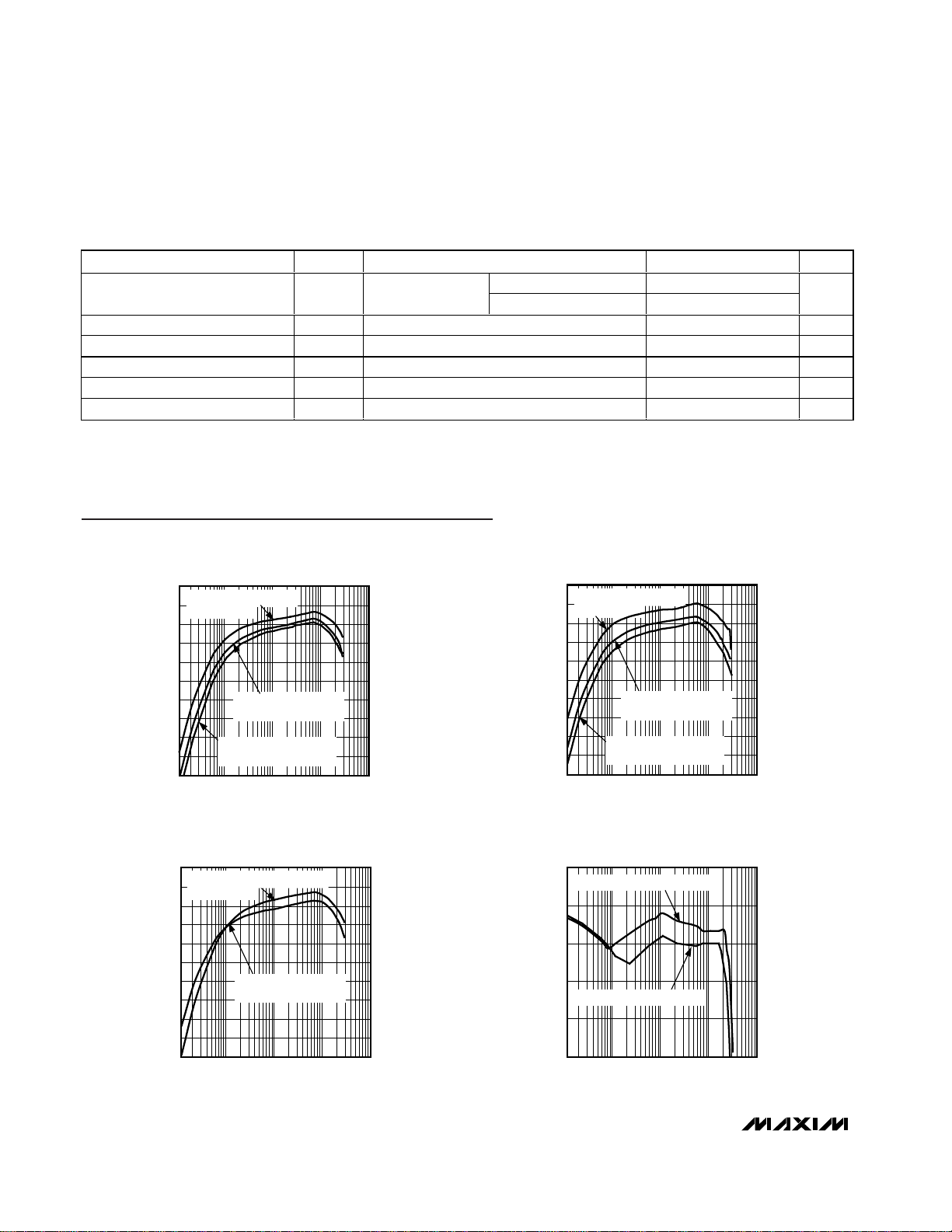
0.001 0.01 0.1 1 10
EFFICIENCY vs. OUTPUT CURRENT
(V
IN
= +5.0V, L = 2.5µH)
MAX1843 toc03
OUTPUT CURRENT (A)
V
OUT
= +1.5V, R
TOFF
= 1OOkΩ,
f
PWM
= 770kHz
V
OUT
= +1.8V, R
TOFF
= 75kΩ,
f
PWM
= 910kHz
V
OUT
= +2.5V, R
TOFF
= 47kΩ,
f
PWM
= 1070kHz
100
95
90
85
80
70
65
60
55
50
75
EFFICIENCY (%)
0.001 0.01 0.1 1 10
EFFICIENCY vs. OUTPUT CURRENT
(V
IN
= +3.3V, L = 1.5µH)
MAX1843 toc04
OUTPUT CURRENT (A)
V
OUT
= +2.5V, R
TOFF
= 56kΩ,
f
PWM
= 1000kHz
V
OUT
= +2.5V, R
TOFF
= 39kΩ,
f
PWM
= 610kHz
V
OUT
= +1.8V, R
TOFF
= 43kΩ,
f
PWM
= 1050kHz
100
95
90
85
80
70
65
60
55
50
75
EFFICIENCY (%)
0.001 0.01 0.1 1 10
EFFICIENCY vs. OUTPUT CURRENT
(f
PWM
= 270kHz)
MAX1843 toc05
I
OUT
(A)
VIN = +3.3V, V
OUT
= +1.8V,
L = 4.7µH, R
TOFF
= 160kΩ
100
95
90
85
80
70
65
60
55
50
75
EFFICIENCY (%)
VIN = +5V, V
OUT
= +1.8V, L = 5.6µH,
R
TOFF
= 240kΩ
NORMALIZED OUTPUT ERROR
vs. OUTPUT CURRENT
MAX1843 toc06
0.001 0.01 0.1 1 10
OUTPUT CURRENT (A)
VIN = +3.3V, V
OUT
= +1.5V, L = 1.5µH
VIN = +5V, V
OUT
= +1.5V, L = 2.5µH
0.1
0
-0.1
-0.2
-0.3
-0.4
NORMALIZED OUTPUT ERROR (%)
PARAMETER
CONDITIONS MIN MAX
V
IN
= +4.5V 150
NMOS Switch On-Resistance R
ON,NILX
= 0.5A
V
IN
= +3V 200
mΩ
Current-Limit Threshold I
LIMIT
2.9 4.3 A
Idle-Mode Current Threshold 0.2 1.0 A
No-Load Supply Current
VFB = 1.2V 600 µA
FB Input Bias Current I
FB
VFB = 1.2V 0 300 nA
Off-Time t
OFF
R
TOFF
= 110kΩ 0.85 1.15 µs
MAX1843
2.7A, 1MHz, Low-Voltage, Step-Down Regulator with
Internal Synchronous Rectification in QFN Package
4 _______________________________________________________________________________________
ELECTRICAL CHARACTERISTICS (continued)
(VIN= VCC= +3.3V, FBSEL = GND, TA= -40°C to +85°C, unless otherwise noted. Typical values are at TA= +25°C.) (Note 3)
Note 2: Recommended operating frequency, not production tested.
Note 3: Specifications from 0°C to -40°C are guaranteed by design, not production tested.
SYMBOL
IIN + I
CC
UNITS
Page 5
MAX1843
2.7A, 1MHz, Low-Voltage, Step-Down Regulator with
Internal Synchronous Rectification in QFN Package
_______________________________________________________________________________________ 5
Typical Operating Characteristics (continued)
(Circuit of Figure 1, TA = +25°C, unless otherwise noted.)
0
1.0
0.5
2.0
1.5
3.0
2.5
3.5
4.5
4.0
5.0
0 100 150 20050 250 300 350 450400 500
OFF-TIME vs. R
TOFF
MAX1843 toc02
R
TOFF
(kΩ)
t
OFF
(µs)
LOAD-TRANSIENT RESPONSE
V
OUTPUT
50mV/div
I
L
2A/div
MAX1843 toc09
10µs/div
0
LINE-TRANSIENT RESPONSE
V
INPUT
2V/div
V
OUTPUT
20mV/div
AC-COUPLED
MAX1843 toc10
20µs/div
I
OUT
= 2.5A, V
OUT
= +1.5V
R
TOFF
= 100kΩ, L = 2.2µH
0
400
200
800
600
1000
1200
0 1.0 1.50.5 2.0 2.5 3.0
SWITCHING FREQUENCY
vs. OUTPUT CURRENT
MAX1843 toc07
OUTPUT CURRENT (A)
FREQUENCY (kHz)
VIN = +5V, V
OUT
= +2.5V, L = 2.5µH
VIN = +3.3V, V
OUT
= +1.5V, L = 1.5µH
VIN = +5V, V
OUT
= +1.5V, L = 2.5µH
0
0
0
0
STARTUP AND SHUTDOWN
V
SS
2V/div
MAX1843 toc08
V
SHDN
5V/div
R
OUT
= 0.5Ω, R
TOFF
= 56kΩ
V
IN
= +3.3V, V
OUT
= +1.5V
I
INPUT
1A/div
V
OUTPUT
1V/div
1ms/div
500
450
(µA)
CC
400
+ I
IN
350
300
250
200
150
100
NO-LOAD SUPPLY CURRENT, I
50
0
021 3456
SUPPLY CURRENT
vs. SUPPLY VOLTAGE
NO LOAD
SHUTDOWN
VIN (V)
MAX1843 toc01
100
(nA)
90
CC
80
+ I
IN
70
60
50
40
30
20
10
SHUTDOWN SUPPLY CURRENT, I
0
Page 6

MAX1843
2.7A, 1MHz, Low-Voltage, Step-Down Regulator with
Internal Synchronous Rectification in QFN Package
6 _______________________________________________________________________________________
Detailed Description
The MAX1843 synchronous, current-mode, constant-offtime, PWM DC-DC converter steps down input voltages
of +3V to +5.5V to a preset output voltage of +2.5V,
+1.8V, or +1.5V, or to an adjustable output voltage from
+1.1V to VIN. It delivers up to 2.7A of output current.
Internal switches composed of a 0.09Ω PMOS power
switch and a 0.07Ω NMOS synchronous-rectifier switch
improve efficiency, reduce component count, and eliminate the need for an external Schottky diode.
The MAX1843 optimizes efficiency by operating in constant-off-time mode under heavy loads and in Maxim’s
proprietary idle mode under light loads. A single resistorprogrammable constant-off-time control sets switching
frequencies up to 1MHz, allowing the user to optimize
performance trade-offs in efficiency, switching noise,
component size, and cost. Under low-dropout conditions,
the device operates in a 100% duty-cycle mode, where
the PMOS switch remains continuously on. Idle mode
enhances light-load efficiency by skipping cycles, thus
reducing transition and gate-charge losses.
When power is drawn from a regulated supply, constantoff-time PWM architecture essentially provides constantfrequency operation. This architecture has the inherent
advantage of quick response to line and load transients.
The MAX1843’s current-mode, constant-off-time PWM
architecture regulates the output voltage by changing
the PMOS switch on-time relative to the constant offtime. Increasing the on-time increases the peak inductor current and the amount of energy transferred to the
load per pulse.
Modes of Operation
The current through the PMOS switch determines the
mode of operation: constant-off-time mode (for load
currents greater than half the idle mode threshold, of
idle mode), or idle mode (for load currents less than
half the idle-mode threshold). Current sense is
achieved through a proprietary architecture that eliminates current-sensing I2R losses.
Pin Description
NAME FUNCTION
2, 4 IN Supply Voltage Input—for the internal PMOS power switch
PIN
3, 18, 19,
23, 25
LX
Connection for the drains of the PMOS power switch and NMOS synchronous-rectifier switch. Connect
the inductor from this node to the output filter capacitor and load.
6 SS Soft-Start. Connect a capacitor from SS to GND to limit inrush current during startup.
7 COMP
Integrator Compensation. Connect a capacitor from COMP to VCCfor integrator compensation. See
Integrator Amplifier section.
8 TOFF
Off-Time Select Input. Sets the PMOS power switch off-time during constant-off-time operation. Connect a
resistor from TOFF to GND to adjust the PMOS switch off-time.
9 FB
Feedback Input—for both preset-output and adjustable-output operating modes. Connect directly to
output for fixed-voltage operation or to a resistive divider for adjustable operating modes.
13, back-
side pad
GND Analog Ground. Connect exposed backside pad to pin 13.
14 REF Reference Output. Bypass REF to GND with a 1µF capacitor.
15 FBSEL Feedback Select Input. Selects output voltage. See Table 2 for programming instructions.
16 V
CC
Analog Supply Voltage Input. Supplies internal analog circuitry. Bypass VCCwith a 10Ω and 2.2µF lowpass filter. See Figure 1.
17, 20, 21 PGND Power Ground. Internally connected to the internal NMOS synchronous-rectifier switch.
1, 5, 10,
11, 12,
22, 24,
26, 28
N.C. Not internally connected.
27
SHDN
Shutdown Control Input. Drive SHDN low to disable the reference, control circuitry, and internal
MOSFETs. Drive high or connect to V
CC
for normal operation.
Page 7

MAX1843
2.7A, 1MHz, Low-Voltage, Step-Down Regulator with
Internal Synchronous Rectification in QFN Package
_______________________________________________________________________________________ 7
Constant-Off-Time Mode
Constant-off-time operation occurs when the current
through the PMOS switch is greater than the idle-mode
threshold current (which corresponds to a load current of
half the idle mode threshold). In this mode, the regulation
comparator turns the PMOS switch on at the end of each
off-time, keeping the device in continuous-conduction
mode. The PMOS switch remains on until the output is in
regulation or the current limit is reached. When the
PMOS switch turns off, it remains off for the programmed
off-time (t
OFF
). To control the current under short-circuit
conditions, the PMOS switch remains off for approximately 4 x t
OFF
when V
OUT
< V
OUT(NOM)
/ 4.
Figure 2. Functional Diagram
Figure 1. Typical Circuit
470pF
10Ω
V
IN
2.2µF
COMP
V
SHDN
INPUT
C
10Ω
2.2µF
REF
g
CC
33µF
470pF
R
TOFF
FEEDBACK
SELECTION
m
REF
IN
IN
V
CC
SHDN
COMP
TOFF
FBSEL
MAX1843
LX
FB
PGND
GND
FBSEL
REF
SS
MAX1843
SUMMING
COMPARATOR
L
1µF
0.01µF
SS
CURRENT
SENSE
SKIP
PWM LOGIC
AND
DRIVERS
OUTPUT
C
OUT
150µF
= +2.5V, FBSEL = V
V
OUT
V
= +1.8V, FBSEL = REF
OUT
= +1.5V, FBSEL = FLOATING
V
OUT
0.01µF
FB
IN
LX
CC
C
IN
CERAMIC
C
OUT
V
IN
+3.0V TO +5.5V
V
OUT
REF
1µF
NOTE: HEAVY LINES DENOTE HIGH-CURRENT PATHS.
REF
GND
TIMER
R
CURRENT
SENSE
PGNDTOFF
TOFF
Page 8

MAX1843
2.7A, 1MHz, Low-Voltage, Step-Down Regulator with
Internal Synchronous Rectification in QFN Package
8 _______________________________________________________________________________________
Idle Mode
Under light loads, this device improves efficiency by
switching to a pulse-skipping idle mode. Idle-mode
operation occurs when the current through the PMOS
switch is less than the idle-mode threshold current. Idle
mode forces the PMOS to remain on until the current
through the switch reaches the idle mode threshold,
thus minimizing the unnecessary switching that
degrades efficiency under light loads. In idle mode, the
device operates in discontinuous conduction. Currentsense circuitry monitors the current through the NMOS
synchronous switch, turning it off before the current
reverses. This prevents current from being pulled from
the output filter through the inductor and NMOS switch to
ground. As the device switches between operating
modes, no major shift in circuit behavior occurs.
100% Duty-Cycle Operation
When the input voltage drops near the output voltage,
the duty cycle increases until the PMOS MOSFET is on
continuously. The dropout voltage in 100% duty cycle
is the output current multiplied by the on-resistance of
the internal PMOS switch and parasitic resistance in the
inductor. The PMOS switch remains on continuously as
long as the current limit is not reached.
Shutdown
Drive SHDN to a logic-level low to place the MAX1843
in low-power shutdown mode and reduce supply current to less than 1µA. In shutdown, all circuitry and
internal MOSFETs turn off, and the LX node becomes
high impedance. Drive SHDN to a logic-level high or
connect to VCCfor normal operation.
Summing Comparator
Three signals are added together at the input of the
summing comparator (Figure 2): an output voltage error
signal relative to the reference voltage, an integrated
output voltage error correction signal, and the sensed
PMOS switch current. The integrated error signal is provided by a transconductance amplifier with an external
capacitor at COMP. This integrator provides high DC
accuracy without the need for a high-gain amplifier.
Connecting a capacitor at COMP modifies the overall
loop response (see the Integrator Amplifier section).
Synchronous Rectification
In a step-down regulator without synchronous rectification, an external Schottky diode provides a path for current to flow when the inductor is discharging. Replacing
the Schottky diode with a low-resistance NMOS synchronous switch reduces conduction losses and
improves efficiency.
The NMOS synchronous-rectifier switch turns on following a short delay after the PMOS power switch turns off,
thus preventing cross-conduction or “shoot through.” In
constant-off-time mode, the synchronous-rectifier switch
turns off just prior to the PMOS power switch turning on.
While both switches are off, inductor current flows
through the internal body diode of the NMOS switch. The
internal body diode’s forward voltage is relatively high.
Thermal Resistance
Junction-to-ambient thermal resistance, θJA, is highly
dependent on the amount of copper area immediately
surrounding the IC leads. The MAX1843 EV kit has 1in
2
of copper area and a thermal resistance of 50°C/W with
no forced airflow. Airflow over the board significantly
reduces the junction-to-ambient thermal resistance. For
heatsinking purposes, it is essential to connect the
exposed backside pad to a large analog ground plane.
Power Dissipation
Power dissipation in the MAX1843 is dominated by
conduction losses in the two internal power switches.
Power dissipation due to supply current in the control
section and average current used to charge and discharge the gate capacitance of the internal switches
(i.e., switching losses) is approximately:
P
DS
= C x V
IN
2
x f
PWM
where C = 2.5nF and f
PWM
is the switching frequen-
cy in PWM mode.
This number is reduced when the switching frequency
decreases as the part enters idle mode. Combined conduction losses in the two power switches are approximated by:
PD= I
OUT
2
x R
PMOS
where R
PMOS
is the on-resistance of the PMOS switch.
The junction-to-ambient thermal resistance required to
dissipate this amount of power is calculated by:
θJA= (T
J,MAX
- T
A,MAX
) / P
D(TOT)
where: θJA= junction-to-ambient thermal resistance
T
J(MAX)
= maximum junction temperature
T
A(MAX)
= maximum ambient temperature
P
D(TOT)
= total losses
Page 9

MAX1843
2.7A, 1MHz, Low-Voltage, Step-Down Regulator with
Internal Synchronous Rectification in QFN Package
_______________________________________________________________________________________ 9
Design Procedure
For typical applications, use the recommended component values in Table 1. For other applications, take the
following steps:
1) Select the desired PWM-mode switching frequency.
See Figure 3 for maximum operating frequency.
2) Select the constant off-time as a function of input
voltage, output voltage, and switching frequency.
3) Select R
TOFF
as a function of off-time.
4) Select the inductor as a function of output voltage,
off-time, and peak-to-peak inductor current.
Setting the Output Voltage
The output of the MAX1843 is selectable between one
of three preset output voltages: +2.5V, +1.8V, and
+1.5V. For a preset output voltage, connect FB to the
output voltage, and connect FBSEL as indicated in
Table 2. For an adjustable output voltage, connect
FBSEL to GND, and connect FB to a resistive divider
between the output voltage and ground (Figure 4).
Regulation is maintained for adjustable output voltages
when VFB= V
REF
. Use a resistor in the 10kΩ to 50kΩ
range for R1. R2 is given by the equation:
where V
REF
is typically 1.1V.
Figure 4. Adjustable Output Voltage
Figure 3. Maximum Recommended Operating Frequency vs.
Input Voltage
V
OUT
(V)
R
TOFF
(kΩ)
2.2 39
L
(µH)
5 3.3
2.2
V
IN
(V)
47
2.2 755 1.8
1.5 393.3 2.5
1.5 433.3 1.8
1.5 563.3 1.5
5 2.5
2.2 1005 1.5
f
PWM
(kHz)
800
850
570
985
940
715
1180
Table 1. Recommended Component
Values (I
OUT
= 2.7A)
Output voltageUnconnected
FBSEL
OUTPUT
VOLTAGE
(V)
FB
Resistive
divider
GND Adjustable
Output voltageREF 1.8
1.5
Output voltage
V
CC
2.5
PIN
Table 2. Output Voltage Programming
MAXIMUM RECOMMENDED
OPERATING FREQUENCY vs. INPUT VOLTAGE
1400
V
= +1.5V
OUT
1200
1000
V
= +1.8V
OUT
800
V
= +2.5V
600
FREQUENCY (kHz)
400
200
0
2.6 3.6 4.13.1 4.6 5.1 5.6
OUT
VIN (V)
V
= +3.3V
OUT
MAX1843 fig03
LX
MAX1843
FB
/ V
OUT
REF
- 1)
R2 = R1(V
= 1.1V
V
REF
R2
R1
V
OUT
R2 R1
=
V
V
OUT
REF
−
1
Page 10

MAX1843
2.7A, 1MHz, Low-Voltage, Step-Down Regulator with
Internal Synchronous Rectification in QFN Package
10 ______________________________________________________________________________________
Programming the Switching Frequency
and Off-Time
The MAX1843 features a programmable PWM mode
switching frequency, which is set by the input and output voltage and the value of R
TOFF
, connected from
TOFF to GND. R
TOFF
sets the PMOS power switch offtime in PWM mode. Use the following equation to select
the off-time according to the desired switching frequency in PWM mode:
where: t
OFF
= the programmed off-time
V
IN
= the input voltage
V
OUT
= the output voltage
V
PMOS
= the voltage drop across the internal
PMOS power switch
V
NMOS
= the voltage drop across the internal
NMOS synchronous-rectifier switch
f
PWM
= switching frequency in PWM mode
Select R
TOFF
according to the formula:
R
TOFF
= (t
OFF
- 0.07µs) (110kΩ / 1.00µs)
Recommended values for R
TOFF
range from 36kΩ to
430kΩ for off-times of 0.4µs to 4µs.
Inductor Selection
The key inductor parameters must be specified: inductor value (L) and peak current (I
PEAK
). The following
equation includes a constant, denoted as LIR, which is
the ratio of peak-to-peak inductor AC current (ripple
current) to maximum DC load current. A higher value of
LIR allows smaller inductance but results in higher losses and ripple. A good compromise between size and
losses is found at approximately a 25% ripple-current
to load-current ratio (LIR = 0.25), which corresponds to
a peak inductor current 1.125 times the DC load current:
where: I
OUT
= maximum DC load current
LIR = ratio of peak-to-peak AC inductor current
to DC load current, typically 0.25
The peak inductor current at full load is 1.125 x I
OUT
if
the above equation is used; otherwise, the peak current
is calculated by:
Choose an inductor with a saturation current at least as
high as the peak inductor current. The inductor you
select should exhibit low losses at your chosen operating
frequency.
Capacitor Selection
The input filter capacitor reduces peak currents and
noise at the voltage source. Use a low-ESR and lowESL capacitor located no further than 5mm from IN.
Select the input capacitor according to the RMS input
ripple-current requirements and voltage rating:
where I
RIPPLE
= input RMS current ripple.
The output filter capacitor affects the output voltage ripple, output load-transient response, and feedback loop
stability. For stable operation, the MAX1843 requires a
minimum output ripple voltage of V
RIPPLE
≥ 1% x V
OUT
.
The minimum ESR of the output capacitor should be:
Stable operation requires the correct output filter capacitor. When choosing the output capacitor, ensure that:
Integrator Amplifier
An internal transconductance amplifier fine tunes the
output DC accuracy. A capacitor, C
COMP
, from COMP
to VCCcompensates the transconductance amplifier.
For stability, choose C
COMP
= 470pF.
A large capacitor value maintains a constant average
output voltage but slows the loop response to changes
in output voltage. A small capacitor value speeds up
the loop response to changes in output voltage but
decreases stability. Choose the capacitor values that
result in optimal performance.
t
=
OFF
fVV V
PWM IN PMOS NMOS
−−
VV V
()
IN OUT PMOS
−
()
+
Vt
OUT OFF
L
=
I LIR
OUT
×
×
II
PEAK OUT
=+
Vt
×
OUT OFF
L
×
2
II
RIPPLE LOAD
=
VVV
OUT IN OUT
−
()
V
IN
ESR
% >×1
t
OFF
L
C
OUT
t
OFF
≥µµ /79
V
OUT
FV s
Page 11

MAX1843
2.7A, 1MHz, Low-Voltage, Step-Down Regulator with
Internal Synchronous Rectification in QFN Package
______________________________________________________________________________________ 11
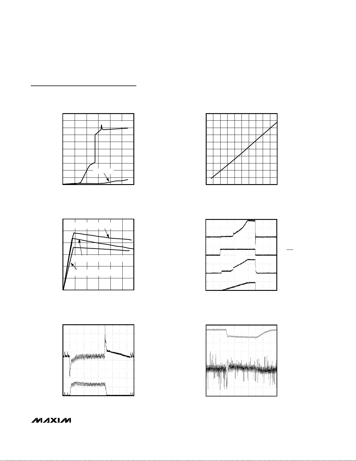
Soft-Start
Soft-start allows a gradual increase of the internal current limit to reduce input surge currents at startup and
at exit from shutdown. A timing capacitor, CSS, placed
from SS to GND sets the rate at which the internal current limit is changed. Upon power-up, when the device
comes out of undervoltage lockout (2.6V typ) or after
the SHDN pin is pulled high, a 4µA constant-current
source charges the soft-start capacitor and the voltage
on SS increases. When the voltage on SS is less than
approximately 0.7V, the current limit is set to zero. As
the voltage increases from 0.7V to approximately 1.8V,
the current limit is adjusted from 0 to the current-limit
threshold (see the Electrical Characteristics). The voltage across the soft-start capacitor changes with time
according to the equation:
The soft-start current limit varies with the voltage on the
soft-start pin, SS, according to the equation:
where I
LIMIT
is the current threshold from the Electrical
Characteristics.
The constant-current source stops charging once the
voltage across the soft-start capacitor reaches 1.8V
(Figure 5).
Frequency Variation with Output Current
The operating frequency of the MAX1843 is determined
primarily by t
OFF
(set by R
TOFF
), VIN, and V
OUT
as
shown in the following formula:
f
PWM
= (VIN- V
OUT
- V
PMOS
) / [t
OFF(VIN
- V
PMOS
+
V
NMOS
)]
However, as the output current increases, the voltage
drop across the NMOS and PMOS switches increases
and the voltage across the inductor decreases. This
causes the frequency to drop. The change in frequency
can be approximated with the following formula:
∆f
PWM
= -I
OUT
x R
PMOS
/ (VINx t
OFF
)
where R
PMOS
is the resistance of the internal MOSFETs
(90mΩ typ).
Circuit Layout and Grounding
Good layout is necessary to achieve the MAX1843’s
intended output power level, high efficiency, and low
noise. Good layout includes the use of ground planes,
careful component placement, and correct routing of
traces using appropriate trace widths. The following
points are in order of decreasing importance:
1) Minimize switched-current and high-current ground
loops. Connect the input capacitor’s ground, the output capacitor’s ground, and PGND. Connect the
resulting island to GND at only one point.
2) Connect the input filter capacitor less than 5mm
away from IN. The connecting copper trace carries
large currents and must be at least 1mm wide,
preferably 2.5mm.
3) Place the LX node components as close together
and as near to the device as possible. This reduces
resistive and switching losses as well as noise.
4) Ground planes are essential for optimum performance. In most applications, the circuit is located on
a multilayer board and full use of the four or more
layers is recommended. For heat dissipation, connect the exposed backside pad to a large analog
ground plane, preferably on a surface of the board
that receives good airflow. If the ground plane is
located on the IC surface, make use of the N.C. pins
adjacent to GND to lower thermal resistance to the
ground plane. If the ground is located elsewhere,
use several vias to lower thermal resistance. Typical
applications use multiple ground planes to minimize
thermal resistance. Avoid large AC currents through
the analog ground plane.
Chip Information
TRANSISTOR COUNT: 3662
Figure 5. Soft-Start Current-Limit Over Time
V
SS
At
=×4µ
C
SS
SSI
LIMIT
VV
− .
07
SS
=×
.
11
V
I
LIMIT
SHDN
0
V
(V)
SS
0
(A)
I
LIMIT
0
0.7V
1.8V
I
t
LIMIT
Page 12

MAX1843
2.7A, 1MHz, Low-Voltage, Step-Down Regulator with
Synchronous Rectification in QFN Package
12 ______________________________________________________________________________________
Package Information
(The package drawing(s) in this data sheet may not reflect the most current specifications. For the latest package outline information,
go to www.maxim-ic.com/packages.)
32L QFN .EPS
Page 13

2.7A, 1MHz, Low-Voltage, Step-Down Regulator with
Internal Synchronous Rectification in QFN Package
MAX1843
Maxim cannot assume responsibility for use of any circuitry other than circuitry entirely embodied in a Maxim product. No circuit patent licenses are
implied. Maxim reserves the right to change the circuitry and specifications without notice at any time.
Maxim Integrated Products, 120 San Gabriel Drive, Sunnyvale, CA 94086 408-737-7600 ____________________ 13
© 2002 Maxim Integrated Products Printed USA is a registered trademark of Maxim Integrated Products.
Package Information (continued)
(The package drawing(s) in this data sheet may not reflect the most current specifications. For the latest package outline information,
go to www.maxim-ic.com/packages.)
Page 14

Copyright © Each Manufacturing Company.
All Datasheets cannot be modified without permission.
This datasheet has been download from :
www.AllDataSheet.com
100% Free DataSheet Search Site.
Free Download.
No Register.
Fast Search System.
www.AllDataSheet.com
 Loading...