

Page 1
General Description
The MAX1838 is a dual, current-limited USB switch with
auxiliary input supply. Each switch meets all IEC specifications for USB ports and is guaranteed to supply
500mA from either of two input supplies. A control pin
selects the power source from either the main or auxiliary supply.
The MAX1838 has multiple protection features, including independent thermal-shutdown on each channel to
limit junction temperature in case of a prolonged short
or overload condition. The device has accurate internal
current-limit and reverse-current protection to safeguard the input supply against overload. When powered from the auxiliary supply, the current limit on each
channel is set independently with an external resistor.
An autoreset feature latches the switch off if the output
is shorted, thereby saving system power. When the
short is removed, the switch automatically turns back
on. Independent fault signals (FAULTA and FAULTB)
notify the microprocessor (µP) that the internal current
limit has been reached. A 20ms fault-blanking feature
prevents the MAX1838 from issuing false alarms to the
host during power-up or when hot-swapping into a
capacitive load.
The MAX1838 is available in a space-saving 16-pin
QSOP. For other USB current-limited switches, refer to
the MAX1693, MAX1694, MAX1812, and MAX1823.
Applications
Desktops
Notebook Computers
USB Ports
Docking Stations
Features
o Dual USB Switch with Auxiliary Input
o Autoreset from Fault Condition
o Guaranteed 500mA Load per Channel
o Programmable Current Limits on Auxiliary Inputs
o Reverse Current Protection
o Thermal Overload Protection
o Built-In 20ms Fault-Blanking
o 4V to 5.5V Range
o Independent FAULT Indicator Outputs
MAX1838
Dual USB Switch with Fault Blanking
and Autoreset
________________________________________________________________
Maxim Integrated Products
1
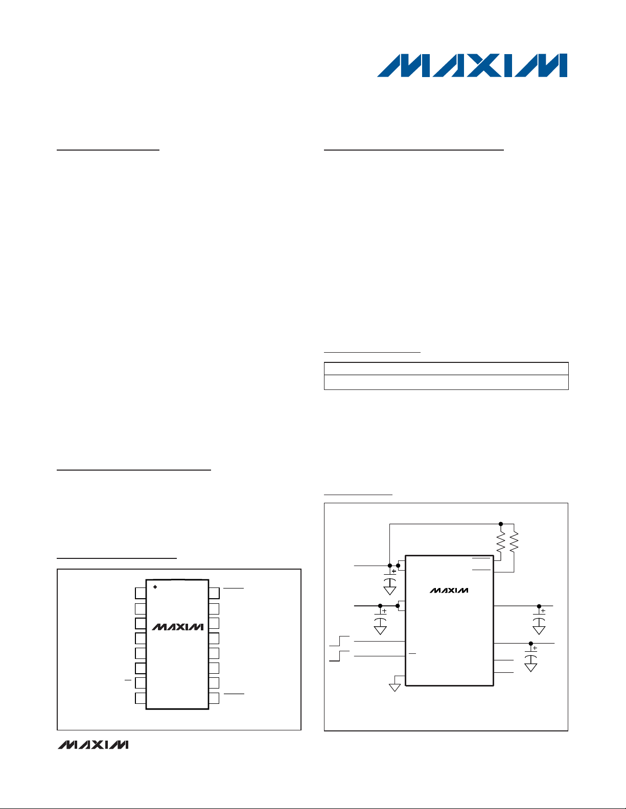
Pin Configuration
Ordering Information
19-2033; Rev 1; 2/10
Typical Operating Circuit
For pricing, delivery, and ordering information, please contact Maxim Direct at 1-888-629-4642,
or visit Maxim’s website at www.maxim-ic.com.
PART TEMP RANGE PIN-PACKAGE
MAX1838EEE -40°C to +85°C 16 QSOP
TOP VIEW
1
GND FAULTA
SEL
2
AUXA
3
4
INA
INB
5
AUXB
6
ON
7
GND
8
16
15
ADJA
14
OUTA2
MAX1838
QSOP
13
12
11
10
9
OUTA1
OUTB2
OUTB1
ADJB
FAULTB
AUX
IN
AUXA
AUXB
INA
INB
SEL
ON
GND
MAX1838
FAULTB
FAULTA
OUTB
OUTA
ADJB
ADJA
OUTB
10µF
OUTA
Page 2
MAX1838
Dual USB Switch with Fault Blanking
and Autoreset
2 _______________________________________________________________________________________
ABSOLUTE MAXIMUM RATINGS
ELECTRICAL CHARACTERISTICS
(V
IN__
= V
AUX__
= 5V, ON = SEL = GND, ADJ_ = open, TA= 0°C to +85°C, unless otherwise noted. Typical values are at TA=
+25°C.)
Stresses beyond those listed under “Absolute Maximum Ratings” may cause permanent damage to the device. These are stress ratings only, and functional
operation of the device at these or any other conditions beyond those indicated in the operational sections of the specifications is not implied. Exposure to
absolute maximum rating conditions for extended periods may affect device reliability.
IN_, AUX_, ON, OUT_, SEL, FAULT_,
ADJ_ to GND .........................................................-0.3V to +6V
IN_, AUX_ to OUTA_; IN_, AUX_ to OUTB_.................-6V to +6V
AUX_ to IN_ .................................................................-6V to +6V
Maximum Continuous Switch Current
(per channel, internally limited).............................................1.2A
FAULT_ Current ..................................................................20mA
Continuous Power Dissipation (T
A
= +70°C)
16-Pin QSOP (derate 8.3mW/°C above +70°C)..........667mW
Operating Temperature Range ...........................-40°C to +85°C
Junction Temperature......................................................+150°C
Storage Temperature Range .............................-65°C to +150°C
Lead Temperature (soldering, 10s) .................................+300°C
Supply Voltage Range
Switch On-Resistance R
AUX_ Standby Supply Current V ON = V
IN_ Standby Supply Current V ON = VIN_13µA
AUX_ Quiescent Supply Current V ON = 0V, I
IN_ Quiescent Supply Current V ON = 0V, I
OUT_ Off-Leakage Current V ON = VIN_, V
Reverse Leakage Current V
Undervoltage Lockout Threshold V
Continuous Load Current 500 mA
Current-Limit Threshold I
Short-Circuit Current Limit I
Continuous Current-Limit
Blanking Timeout Period
Short-Circuit Blanking Timeout
Period
PARAMETER SYMBOL CONDITIONS MIN TYP MAX UNITS
V
IN_
V
AUX_
ON
UVLO
LIM
SHORT
VIN_ = 5V, each switch 95 170
VIN_ = 4V, each switch 100
AUX
= 5.5V, VIN_ = V
OUT
VIN_ or V
VIN_ - V
V
R
SEL = GND,
V
(I
SEL = AUX_, V
From continuous current-limit condition to
FAULT_ assertion
From short-circuit current-limit condition to
FAULT_ assertion
AUX
OUT
_ - V
AUX
ADJ
OUT
OUT
OUT
_ = 67kΩ 0.09 0.225 0.36
_ = 0V
_ pulsing)
4.0 5.5
4.0 5.5
_ 7 16 µA
_ = 0A 66 350 µA
OUT
_ = 0A, SEL = AUX_ 23 300 µA
OUT
_ = V
OUTA
_ rising edge, 3% hysteresis 3.0 3.5 3.8 V
_ = 0.5V, SEL = AUX_ 0.6 0.9 1.2
_ = 0.5V, SEL = GND 0.6 0.9 1.2
_ = 0V
OUT
_ = 0V 0.02 10 µA
OUTB
_ = 0V 0.02 10 µA
AUX
0.3 0.48 A
R
_ = 67kΩ
ADJ
0.6 1.2 1.8 A
10 20 35 ms
7.5 18 35 ms
0.09 A
0.35 A
V
mΩ
A
PEAK
RMS
PEAK
RMS
Page 3
MAX1838
Dual USB Switch with Fault Blanking
and Autoreset
_______________________________________________________________________________________ 3
ELECTRICAL CHARACTERISTICS (continued)
(V
IN__
= V
AUX__
= 5V, ON = SEL = GND, ADJ_ = open, TA= 0°C to +85°C, unless otherwise noted. Typical values are at TA=
+25°C.)
ELECTRICAL CHARACTERISTICS
(V
IN__
= V
AUX__
= VON= 5V, SEL = GND, ADJ_ = open, TA= -40°C to +85°C, unless otherwise noted. Circuit of Figure 1.) (Note 2)
Turn-On Delay
Output Rise Time
Turn-Off Delay from ON
Output Fall Time
Thermal Shutdown Threshold 10°C hysteresis 160 °C
Logic Input High Voltage VIN_ = 4V to 5.5V 2 V
Logic Input Low Voltage VIN_ = 4V to 5.5V 0.8 V
Logic Input Current V ON = 0V or 5.5V -1 1 µA
FAULT_ Output Low Voltage VIN_ = 4V, sinking 1mA 0.4 V
FAULT_ Output High Leakage
Current
Autoreset Current In latched-off state, V
Autoreset Threshold In latched-off state, V
Autoreset Blanking Time In latched-off state, V
AUX_ to IN_ or IN_ to AUX_
Select Delay
PARAMETER SYM BOL CONDITIONS MIN TYP MAX UNITS
= 10Ω, does not include rise time
R
OUT_
(from ON asserted to V
V
R
C
R
IN
OUT
OUT
OUT
_), C
_ = 1µF
OUT
_ = 10Ω, from 10% to 90% of V
_ = 1µF
_ = 10Ω, does not include fall time
(from ON asserted to V
V
R
C
V
IN
OUT
OUT
IN
_), C
_ = V
_ = 1µF
OUT
_ = 10Ω, from 90% to 10% of V
_ = 1µF
FAULT_
OUT
OUT_
= 5.5V 1 µA
_ = 0V 10 25 50 mA
OUT
_ rising 0.4 0.5 0.6 V
OUT
_ > 1V 10 20 35 ms
OUT
_ = 10% of
OUT_
= 90% of
OUT
0.5 2 4.0 ms
,
4.5 ms
0.8 3 ms
_,
3ms
Make-before-break (Note 1) 4.5 9 18 ms
Supply Voltage Range
Switch On-Resistance R
AUX_ Standby Supply Current V
IN_ Standby Supply Current V
AUX_ Quiescent Supply Current V
IN_ Quiescent Supply Current V
OUT_ Off-Leakage Current V
Reverse Leakage Current V
Undervoltage Lockout Threshold V
Continuous Load Current 500 mA
PARAMETER SYM BO L CONDITIONS MIN MAX UNITS
VIN_ 4.0 5.5 V
_ 4.0 5.5 V
V
AUX
VIN_ = 5V, each switch 170 mΩ
ON
UVLOVIN
= V
ON
= VIN_3µA
ON
= 0V, I
ON
= 0V, I
ON
= VIN_, V
ON
OUT
_ or V
_16µA
AUX
= 0A 350 µA
OUT_
= 0A, SEL = AUX_ 300 µA
OUT
_ = V
OUTA
_ = 5.5V, VIN_ = V
_ rising edge, 3% hysteresis 3.0 3.8 V
AUX
_ = 0V 10 µA
OUTB
_ = 0V 10 µA
AUX
Page 4
MAX1838
Dual USB Switch with Fault Blanking
and Autoreset
4 _______________________________________________________________________________________
ELECTRICAL CHARACTERISTICS (continued)
(V
IN__
= V
AUX__
= VON= 5V, SEL = GND, ADJ_ = open, TA= -40°C to +85°C, unless otherwise noted. Circuit of Figure 1.) (Note 2)
Note 1: SEL delay includes both make and break delay. The host system should wait for at least this interval before turning off the
appropriate input supply.
Note 2: Specifications from 0°C to -40°C are guaranteed by design, not production tested.
Current-Limit Threshold I
Short-Circuit Current Limit I
Continuous Current-Limit
Blanking Timeout Period
Short-Circuit Blanking Timeout
Period
Turn-On Delay
Turn-Off Delay from ON
Logic Input High Voltage VIN_ = 4V to 5.5V 2 V
Logic Input Low Voltage VIN_ = 4V to 5.5V 0.8 V
Logic Input Current V ON = 0V or 5.5V -1 1 µA
FAULT_ Output Low Voltage VIN_ = 4V, sinking 1mA 0.4 V
FAULT_ Output High Leakage
Current
Autoreset Current In latched-off state, V
Autoreset Threshold In latched-off state, V
Autoreset Blanking Time In latched-off state, V
AUX_ to IN_ or IN_ to AUX_
Select Delay
PARAMETER SYM BO L CONDITIONS MIN MAX UNITS
LIM
SHORT
VIN_ – V
V
AUX
SEL = GND, V
SEL = AUX_, V
From continuous current-limit condition to
FAULT_ assertion
From short-circuit current-limit condition to
FAULT_ assertion
R
OUT
(from ON asserted to V
_), C
V
IN
R
OUT
(from ON asserted to V
V
_), C
IN
V
_ = V
IN
Make-before-break (Note 1) 4.5 18 ms
_ = 0.5V, SEL = AUX_ 0.6 1.2
OUT
_ – V
_ = 0.5V, SEL = GND 0.6 1.2
OUT
_ = 0V (I
OUT
_ = 0V 0.6 1.8
OUT
_ = 10Ω, does not include rise time
_ = 1µF
OUT
_ = 10Ω, does not include fall time
_ = 1µF
OUT
= 5.5V 1 µA
FAULT_
OUT
OUT
OUT
_ pulsing) 0.6 1.8
OUT
940ms
740ms
_ = 10% of
OUT
_ = 90% of
OUT
_ = 0V 10 55 mA
_ rising 0.4 0.6 V
_ > 1 V 9 40 ms
0.5 4 ms
A
A
PEAK
3ms
Page 5

MAX1838
Dual USB Switch with Fault Blanking
and Autoreset
_______________________________________________________________________________________
5
Typical Operating Characteristics
(Circuit of Figure 2, V
IN_
= 5V, TA= +25°C, unless otherwise noted.)
AUX QUIESCENT CURRENT vs. V
70
60
SEL = GND
50
40
30
20
AUX QUIESCENT CURRENT (µA)
10
0
023145
VIN = 4.5V
VIN = 5V
V
AUX
IN + AUX QUIESCENT CURRENT
vs. TEMPERATURE
110
SEL = GND
100
90
QUIESCENT CURRENT (µA)
80
70
-40 20 40-20 0 60 80
TEMPERATURE (°C)
(V)
VIN = V
VIN = V
VIN = V
VIN = 0
VIN = 5.5V
= 5.5V
AUX
= 5V
AUX
= 4.5V
AUX
AUX
MAX1838 toc01
MAX1838 toc04
IN QUIESCENT CURRENT vs. V
30
SEL = AUX
25
20
15
10
IN QUIESCENT CURRENT (µA)
5
0
023145
VIN = 5V
V
AUX
(V)
IN + AUX QUIESCENT SHUTDOWN CURRENT
vs. TEMPERATURE
10.0
9.5
VIN = V
9.0
8.5
8.0
7.5
SHUTDOWN CURRENT (µA)
7.0
6.5
VIN = V
6.0
-40 0-20 20406080
VIN = V
= 4.5V
AUX
= 5.5V
AUX
TEMPERATURE (°C)
VIN = 5.5V
= 5.0V
AUX
AUX
MAX1838 toc02
VIN = 4.5V
MAX1838 toc05
IN + AUX QUIESCENT CURRENT
vs. TEMPERATURE
100
SEL = AUX = IN
90
V
80
QUIESCENT CURRENT (µA)
70
-40 20 40-20 0 60 80
TEMPERATURE (°C)
V
= 5V
AUX
V
= 4.5V
AUX
SWITCH LEAKAGE CURRENT
vs. TEMPERATURE, FULL DATA
1000
100
IN = AUX = SEL = ON = GND
= 5.5V
V
OUT_
10
VIN = V
= VON = V
SWITCH LEAKAGE CURRENT (nA)
1
-40 80
AUX
OUT_ = GND
020-20 40 60
TEMPERATURE (°C)
AUX
= 5.5V
SEL
MAX1838 toc03
MAX1838 toc06
= 5.5V
NORMALIZED SWITCH ON-RESISTANCE
vs. TEMPERATURE
1.3
1.2
1.1
I
= 500mA
1.0
0.9
NORMALIZED ON-RESISTANCE (Ω)
0.8
0.7
-40 20 40-20 0 60 80
OUT_
TEMPERATURE (°C)
CONTINUOUS CURRENT LIMIT THRESHOLD
vs. TEMPERATURE
0.94
MAX1838 toc07
0.92
0.90
0.88
CONTINUOUS CURRENT LIMIT THRESHOLD (A)
0.86
-40 20-20 0 40 60 80
TEMPERATURE (°C)
2.3
MAX1838 toc08
2.2
2.1
2.0
TURN-ON DELAY (ms)
1.9
1.8
TURN-ON DELAY vs. TEMPERATURE
SEL = GND
VIN = V
= 5.0V
AUX
VIN = V
= 5.5V
AUX
-40 0-20 20 40 60 80
TEMPERATURE (°C)
VIN = V
AUX
= 4.5V
MAX1838 toc09
Page 6

MAX1838
Dual USB Switch with Fault Blanking
and Autoreset
6 _______________________________________________________________________________________
Typical Operating Characteristics (continued)
(Circuit of Figure 2, V
IN_
= 5V, TA= +25°C, unless otherwise noted.)
18.5
19.0
19.5
20.0
20.5
FAULT-BLANKING TIME vs. TEMPERATURE
MAX1838 toc10
TEMPERATURE (°C)
FAULT-BLANKING TIME (ms)
-40 20 40-20 0 60 80
V
AUX
= 5.0V
V
AUX
= 4.5V
V
AUX
= 5.5V
15
20
30
25
35
40
-40 0-20 20 40 60 80
AUTORESET CURRENT vs. TEMPERATURE
MAX1838 toc11
TEMPERATURE (°C)
AUTORESET CURRENT (mA)
VIN = V
AUX
= 5.5V
VIN = V
AUX
= 4.5V
0
10
5
20
15
30
25
35
0 1.0 1.5 2.00.5 2.5 3.0 3.5 4.0 4.5 5.0 5.5
AUTORESET CURRENT vs. INPUT VOLTAGE
MAX1838 toc12
INPUT VOLTAGE (V)
AUTOREST CURRENT (mA)
AUX = IN,
SEL = ON = GND
10ms/div
OVERLOAD RESPONSE INTO 2.5Ω LOAD
5V
5V
V
FAULT_
I
OUT_
0.5A/div
V
OUT_
0
0
0
MAX1838 toc13
0.5A/div
1ms/div
OVERLOAD RESPONSE INTO 2.5Ω LOAD
(EXPANDED TIME SCALE)
5V
5V
V
FAULT_
I
OUT_
V
OUT_
0
0
0
MAX1838 toc14
0.5A/div
10ms/div
SHORT-CIRCUIT RESPONSE INTO 0Ω
5V
5V
V
FAULT_
I
OUT_
0.5A
V
OUT_
0
0
1A
0
MAX1838 toc15
1ms/div
SHORT-CIRCUIT RESPONSE INTO 0Ω
(EXPANDED TIME SCALE)
5V
5V
V
FAULT_
V
OUT_
0
0
MAX1838 toc16
I
OUT_
0.5A
0
1A
Page 7

MAX1838
Dual USB Switch with Fault Blanking
and Autoreset
_______________________________________________________________________________________ 7
Typical Operating Characteristics (continued)
(Circuit of Figure 2, V
IN_
= 5V, TA= +25°C, unless otherwise noted.)
1ms/div
SWITCH TURN-OFF TIME,
C
OUT
= 1µF R
OUT
= 10Ω
MAX1838 toc18
5V
5V
V
OUT_
0
1V
2V
3V
4V
0
V
ON
1ms/div
START-UP TIME INTO 10Ω LOAD
4V
5V
V
OUT_
I
OUT_
0
0.5A
0
2V
0
MAX1838 toc19
V
ON
Pin Description
SWITCH TURN-ON TIME, C
PIN NAME FUNCTION
1, 8 GND Ground. Connect both GND pins together.
2 SEL
3, 6 AUXA, AUXB
4, 5 INA, INB
7 ON
9 FAULTB
= 1µF
OUT
MAX1838 toc17
5V
V
ON
0
5V
4V
3V
V
OUT_
2V
1V
0
1ms/div
Select Input. Control input to select from either V
power from IN source, low for power from AUX source.
Auxiliary Input. Connect both AUX pins together and bypass with a 0.1µF capacitor to ground.
Load conditions may require additional bulk capacitance to maintain AUX voltage regulation.
Power Input. Connect both IN pins together and bypass with a 0.1µF capacitor to GND. Load
conditions may require additional bulk capacitance to maintain the IN voltage regulation.
Control Input. A logic low at ON turns on the device. A logic high shuts off both outputs and all
power to internal circuits. Driving ON higher than IN does not cause damage.
Fault Indicator Output for Channel B. This open-drain output goes low when channel B is in
thermal shutdown or in undervoltage lockout or in a sustained (>20ms) current-limit or short-circuit
condition.
IN_
or V
for both outputs. Pull SEL high for
AUX_
10 ADJB
11, 12 OUTB1, OUTB2
13, 14 OUTA1, OUTA2
Current-Limit Adjust for Channel B. When operating from auxiliary input, adjust the current limit by
connecting a resistor from ADJB to GND as shown in Programmable Current Limit.
Power Output B. Connect both OUTB_ pins together. Connect a 1µF or greater capacitor from
OUTB_ to ground. Load condition may require additional bulk capacitance.
Power Output A. Connect both OUTA_ pins together. Connect a 1µF or greater capacitor from
OUTA_ to ground. Load condition may require additional bulk capacitance.
Page 8

MAX1838
Detailed Description
The MAX1838 is a dual, current-limited switch with
auxiliary inputs designed for USB applications. It has
two independent channels, each with its own faultblanking and autoreset function. Each channel has an
error flag output to notify the USB controller when the
current limit, short circuit, undervoltage lockout, or thermal shutdown threshold is reached. A single input
enables both channels. The MAX1838 supplies the outputs from one of two inputs, IN or AUX, selected by
SEL (Table 1).
The MAX1838 operates from 4V to 5.5V input voltage
range and guarantees a 500mA (min) output current. A
0.9A built-in current limit limits the current in the event
of a heavy overload condition. When powering the
switches from the auxiliary input, each channel has an
adjustable current limit. The MAX1838 has independent
thermal shutdown for each channel in the event of a
prolonged overload or short-circuit condition. The
autoreset function monitors the overload and automatically turns the switch on when the overload is removed.
Use of internal, low-RONNMOS switches enables the
MAX1838 to provide four switches in the small 16-pin
QSOP package. Internal micropower charge pumps
generate the gate drive of these high-side switches.
Separate current limiting and thermal shutdown circuits
permit each switch to operate independently, improving system robustness.
Input Voltage Requirements and
Undervoltage Lockout
The MAX1838 operates in one of three modes (Table 1).
The device receives its supply current from the AUX
input. When V
AUX_
falls below the 3.8V undervoltage
lockout voltage, the MAX1838 shuts down to prevent
erroneous switch operation.
Dual USB Switch with Fault Blanking
and Autoreset
8 _______________________________________________________________________________________
Figure 1. Simplified Functional Diagram
Pin Description (continued)
Table 1. MAX1838 Operation Modes
PIN NAME FUNCTION
15 ADJA
16 FAULTA
Current-Limit Adjust for Channel A. When operating from auxiliary input, adjust the current limit by
connecting a resistor from ADJA to GND as shown in Programmable Current Limit.
Fault Indicator Output for Channel A. This open-drain output goes low when channel A is in
thermal shutdown or undervoltage lockout or in a sustained (>20ms) current-limit or short-circuit
condition.
FAULT LOGIC
20ms
BLANKING
CHANNEL A CONTROL
CIRCUITRY
CHANNEL B CONTROL
CIRCUITRY
20ms
BLANKING
FAULT LOGIC
FAULTA
N
ADJA
OUTA1
OUTA2
OUTB2
OUTB1
ADJB
FAULTB
N
SEL
AUX
IN
ON
THERMAL
SHUTDOWN A
IC POWER
THERMAL
SHUTDOWN B
Power from IN
(SEL high)
Power from AUX
(SEL low)
Full Shutdown
(ON high)
Both A and B outputs receive
current from IN. The IC is powered
from AUX.
Both A and B outputs receive
current from AUX. The IC is
powered from AUX. V
to zero in this mode.
Both A and B outputs are open and
no power is available. Either V
V
may drop to zero.
AUX_
may drop
IN_
IN_
or
Page 9

Output Fault Protection
The MAX1838 senses the switch output voltage and
selects 0.9A continuous current limiting when V
OUT
is
greater than 1V or short-circuit current limiting when
V
OUT
is less than 1V (see
Behavior During Current Limit
and Fault Blanking
).
Autoreset Mode
The MAX1838 monitors the output to detect an overload condition. If an output fault is detected for more
than the 20ms blanking time, OUT_ latches, FAULT
goes low, and OUT sources 25mA to the load. If the
voltage at OUT exceeds 0.5V for 20ms, the fault resets,
the 25mA current source shuts down, and the channel
turns back on. For proper autoreset function, the output
load current must remain below 25mA when the output
voltage is lower than 0.5V. Toggle ON to manually reset
the output.
Thermal Shutdown
The MAX1838 features independent thermal shutdown
for each channel, allowing one channel to deliver
power even if the other channel has a fault condition.
When the junction temperature exceeds +160°C, the
switch turns off and FAULT_ goes low immediately.
Fault blanking does not occur during thermal limit.
When the junction cools by 15°C, the channel turns on
again. If the fault overload condition continues, the
channel cycles on and off, resulting in a pulsed output.
Fault Indicators
The MAX1838 provides an open-drain fault output
(FAULT) for each channel. For most applications, con-
nect FAULT to AUX through a 100kΩ pullup resistor.
FAULT goes low when any one of the following conditions occurs:
• V
AUX
_ is below the undervoltage-lockout (UVLO)
threshold.
• V
IN
_ is below the undervoltage-lockout threshold
and SEL = AUX.
• The switch junction temperature exceeds the thermal
shutdown temperature limit of +160°C.
• The switch is in current-limit or short-circuit limit
mode after the fault-blanking period is exceeded
(autoreset).
After the fault condition is removed, the FAULT output
deasserts after a 20ms delay. Ensure that the MAX1838
has adequate input bypass capacitance to prevent
glitches from triggering FAULT outputs. Input glitches
greater than 0.2V/µs may cause erroneous FAULT indi-
cations.
Programmable Current Limit
When using the auxiliary input (AUX), each channel has
an adjustable current limit. For maximum current limit
(0.9A), open ADJ. For current limits below 0.9A, connect a resistor from ADJ to GND according to the following equation:
I
OUT
_ = 0.9A × R
ADJ
/ (200kΩ + R
ADJ
)
Behavior During Current Limit
and Fault Blanking
The MAX1838 limits switch current in the following
ways. When ON is high, both channels are off. When
ON is low, both channels can supply a continuous output current of at least 500mA. When the output current
exceeds the 0.9A threshold, the MAX1838 will limit the
current depending on the output voltage. If V
OUT
is
greater than 1V (current-limit mode), the MAX1838 regulates the output current to 0.9A. If V
OUT
is less than 1V
(short-circuit mode), the MAX1838 pulses the output,
decreasing the current to 0.35A
RMS
(Table 2). Note that
a thermal overload may result from either of these highcurrent conditions.
The MAX1838 switches may enter current limit in normal operation when powering up or driving heavy
capacitive loads. To differentiate these conditions from
short circuits or sustained overloads that may damage
the device, the MAX1838 has an independent faultblanking circuit in each channel. When a load transient
causes the device to enter current limit, an internal
counter starts to monitor the duration of the fault. If the
load fault persists beyond the 20ms fault-blanking time,
the channel turns off, FAULT asserts low, and the channel enters autoreset mode (see
Autoreset Mode
). Only
current-limit and short-circuit faults are blanked.
Thermal overload faults and input undervoltage immediately cause the channel to turn off and FAULT to
assert low.
Fault blanking allows the MAX1838 to accommodate
USB loads that may not be fully compliant with the USB
specifications. USB loads with additional bypass
capacitance and/or large startup currents can be successfully powered while protecting the upstream power
source. If the switch is able to bring up the load within
the 20ms blanking period, no fault is indicated.
Switching Supplies
To select IN as the source for both channels, drive SEL to
a logic high. To select AUX, drive SEL low. To minimize
switching transients, the MAX1838 switches between
input supplies (IN and AUX) with a make-before-break
sequence. Both switches are on simultaneously for up to
9ms before the initial supply is disconnected. When
switching from IN to AUX, a significant current may flow
MAX1838
Dual USB Switch with Fault Blanking
and Autoreset
_______________________________________________________________________________________ 9
Page 10

MAX1838
between IN and AUX. However, a fault does not trigger
since the fault blanking-time is longer than the supply
switchover time.
Applications Information
Input Power Source
AUX provides the power for the MAX1838 internal control circuitry. Limit the input-voltage slew rate to less
than 0.2V/µs to prevent erroneous FAULT indications.
Input Capacitor
To limit the input voltage drop during momentary output
short-circuit conditions, connect a capacitor from both
AUX and IN to ground. A 0.1µF ceramic capacitor is
required for local decoupling; however, higher capacitor values will further reduce the voltage drop at the
input (Figure 2). When driving inductive loads, a larger
capacitance prevents voltage spikes from exceeding
the MAX1838’s absolute maximum ratings.
Output Capacitor
An output capacitor helps prevent parasitic inductance
from pulling OUT negative during turn-off. When starting up into very large capacitive loads, the switch pulses the output current at 0.35A
RMS
until the output
voltage rises above 1V, then the capacitor continues to
charge at the full 0.9A current limit. There is no limit to
the size of output capacitor, but to prevent a startup
fault assertion, the capacitor must charge up within the
fault-blanking delay period. Typically starting up into a
330µF or smaller capacitor does not trigger a fault output. In addition to bulk capacitance, small value (0.1µF
or greater) ceramic capacitors improve the output’s
resilience to electrostatic discharge (ESD).
Driving Inductive Loads
A wide variety of devices (mice, keyboards, cameras,
and printers) can load the USB port. These devices
commonly connect to the port with cables, which can
add an inductive component to the load. This inductance causes the output voltage at the USB port to ring
Dual USB Switch with Fault Blanking
and Autoreset
10 ______________________________________________________________________________________
Table 2. MAX1838 Current Limiting and Fault Behavior
CONDITION MAX1838 BEHAVIOR
• If a short circuit is detected at the output, the channel turns off, the blanking timer
begins, and FAULT stays high.
• If the short circuit persists during the fault-blanking period, the output pulses at 0.35A
. When the short is removed before the 15ms short-circuit blanking timeout period,
If a short circuit is present
(V
< 1V)
OUT
RMS
the next ramped current pulse soft-starts the output. The FAULT flag stays high.
• If the short circuit persists after the fault-blanking period, FAULT goes low, autoreset
mode is enabled, and the output sources 25mA. If the voltage on that output is above
0.5V for 20ms, the channel resets, the output turns on, and FAULT goes high (see
Short-Circuit Response in the Typical Operating Characteristics.)
-
• Output current regulates at I
• Continuous current at I
If an overload current is present
> 1V)
(V
OUT
If thermal fault condition is present
or the 20ms continuous current-limit timeout period is reached.
• If overcurrent is still present at 20ms, FAULT goes low, autoreset mode is enabled, and
the output sources 25mA. If the voltage on that output is above 0.5V for 20ms, the
channel resets, the output turns on, and FAULT goes high.
• FAULT immediately goes low (the blanking timer does not apply to thermal faults), and
the channel turns off. When the junction cools by 15
removed, autoreset mode is enabled, the output sources 25mA, and FAULT remains
low. If the voltage on that output is above 0.5V for 20ms, the channel resets, the output
turns on, and FAULT goes high.
LIM
, the blanking timer turns on, and FAULT stays high.
LIM
persists until the overload is removed, a thermal fault occurs,
o
C, the thermal fault condition is
Page 11

during a load step. The MAX1838 is capable of driving
inductive loads, but avoid exceeding the device’s
absolute maximum ratings. Usually the load inductance
is relatively small, and the MAX1838’s input includes a
substantial bulk capacitance from an upstream regulator
as well as local bypass capacitors, limiting overshoot. If
severe ringing occurs due to large load inductance,
clamp the MAX1838’s output below 6V and above -0.3V.
Turn-On and Turn-Off Behavior
In absence of faults, the MAX1838’s internal switches
turn on and off slowly under the control of the ON input.
The slow charge-pump switch-drive minimizes load transients on the upstream power source. Under thermal
fault and undervoltage lockout, the power device turns
off rapidly to protect the switch and the power source.
Layout and Thermal Dissipation
To optimize the switch response to output short-circuit
conditions, keep all traces as short as possible to reduce
the effect of undesirable parasitic inductance. Place
input and output capacitors no more than 5mm from
device leads. IN, AUX, and OUT pins must be connected with short traces to the power bus. Wide power bus
planes provide superior switch heat dissipation. While
the switches are on, power dissipation is small and the
package temperature rise is minimal. Calculate the
power dissipation for this condition as follows:
P = (I
OUT
)2R
ON
For the normal operating current (I
OUT
= 0.5A), the maximum on-resistance of the switch is 170mΩ, and the
power dissipation is:
P = (0.5A)
2
x 0.170Ω = 43mW per switch
The worst-case power dissipation occurs when the
switch is in current limit and the output is greater than
1V. In this case, the power dissipated in each switch is
the voltage drop across the switch multiplied by the current limit:
P = (I
LIM
) (VIN- V
OUT
)
For a 5V input and 1V output, the maximum power dissipation per switch is:
P = (1.2A) (5.5V - 1V) = 5.4W
Since the package power dissipation is only 667mW, the
MAX1838 die temperature will exceed the thermal shutdown threshold and the switch output shuts down until
the junction temperature cools by 10°C. The duty cycle
and period are strong functions of the ambient temperature and the PC board layout.
A short circuit at the output causes the power dissipated
across the switch and the junction temperature to
increase. If the fault condition persists, the thermal-overload-protection circuitry activates, and the output shuts
down until the junction temperature decreases by 10°C
(see
Thermal Shutdown
).
MAX1838
Dual USB Switch with Fault Blanking
and Autoreset
______________________________________________________________________________________ 11
Figure 2. Typical Application Circuit
AUX
0.1µF
IN
0.1µF
AUXA
AUXB
INA
INB
SEL
ON
GND
MAX1838
100kΩ
FAULTB
FAULTA
OUTB2
OUTB1
OUTA2
OUTA1
ADJB
ADJA
67kΩ
100kΩ
OUTB
10µF
OUTA
10µF
67kΩ
Page 12

MAX1838
Dual USB Switch with Fault Blanking
and Autoreset
12 ______________________________________________________________________________________
Chip Information
PROCESS: BiCMOS
Package Information
For the latest package outline information and land patterns, go
to www.maxim-ic.com/packages
. Note that a “+”, “#”, or “-” in
the package code indicates RoHS status only. Package drawings may show a different suffix character, but the drawing pertains to the package regardless of RoHS status.
PACKAGE TYPE PACKAGE CODE DOCUMENT NO.
16 QSOP E16-5
21-0055
Page 13

MAX1838
Dual USB Switch with Fault Blanking
and Autoreset
Maxim cannot assume responsibility for use of any circuitry other than circuitry entirely embodied in a Maxim product. No circuit patent licenses are
implied. Maxim reserves the right to change the circuitry and specifications without notice at any time.
Maxim Integrated Products, 120 San Gabriel Drive, Sunnyvale, CA 94086 408-737-7600 ____________________
13
© 2010 Maxim Integrated Products Maxim is a registered trademark of Maxim Integrated Products, Inc.
Revision History
REVISION
NUMBER
0 4/01 Initial release —
1 2/10 Removed UL Certification Pending bullet from Features section 1
REVISION
DATE
DESCRIPTION
PAGES
CHANGED
 Loading...