

Page 1
General Description
The MAX1823 is a dual, current-limited switch with
autoreset specifically made for USB applications. The
autoreset feature latches the switch off if the output is
shorted, saving system power. The switch reactivates
when the short circuit is removed. Each channel is guaranteed to supply 720mA and meet USB specifications.
Low quiescent supply current (50µA) and standby current
(3µA) conserve battery power in portable applications.
The MAX1823 has multiple safety features to ensure
that the USB port is protected. Built-in thermal-overload
protection limits power dissipation and junction temperature. Accurate internal current-limiting circuitry protects the input supply against both overload and
short-circuit conditions. Independent fault signals
(FAULTA and FAULTB) notify the microprocessor (µP)
when a thermal-overload, current-limit, undervoltagelockout (UVLO), or short-circuit fault occurs. A 20ms
fault-blanking feature ignores momentary faults, such
as those caused when hot swapping a capacitive load,
preventing false alarms to the host system. The
MAX1823A/MAX1823B also block reverse current (current from OUT_ to IN_) while in shutdown.
The MAX1823 is available in a space-saving 10-pin
µMAX package. The MAX1823/MAX1823A are enabled
with an active-low signal, and the MAX1823B/MAX1823H
are enabled with an active-high signal. For a single version of this device, refer to the MAX1946 data sheet. For
a triple version, refer to the MAX1940 data sheet.
Applications
USB Ports and Hubs
Notebook and Desktop Computers
PDAs and Palmtop Computers
Docking Stations
Features
♦ Dual USB Switch in Tiny 10-Pin µMAX Package
♦ Autoreset Feature Saves Power
♦ Guaranteed 720mA Load per Channel
♦ Built-In 20ms Fault Blanking
♦ Compliant to USB Specification
♦ Blocks Reverse Current in Shutdown
(MAX1823A/MAX1823B)
♦ 4V to 5.5V Input Voltage Range
♦ Independent Shutdown Control
(MAX1823/MAX1823A—Active Low)
(MAX1823B/MAX1823H—Active High)
♦ Independent FAULT Indicator Outputs
♦ Thermal-Overload Protection
♦ 50µA Quiescent Current (Both Switches On)
♦ 3µA Standby Current
♦ UL Recognized
MAX1823/MAX1823A/MAX1823B/MAX1823H
Dual USB Switch with Fault
Blanking and Autoreset
________________________________________________________________ Maxim Integrated Products 1
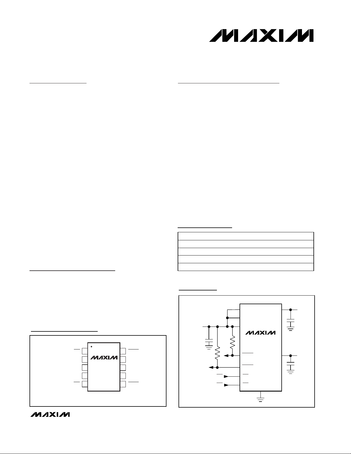
Ordering Information
Typical Operating Circuit
19-1903; Rev 3; 10/03
Pin Configuration
For pricing, delivery, and ordering information, please contact Maxim/Dallas Direct! at
1-888-629-4642, or visit Maxim’s website at www.maxim-ic.com.
TOP VIEW
INA
1
2
MAX1823
3
IN
4
5
MAX1823A
MAX1823B
MAX1823H
µMAX
10
9
8
7
6
FAULTA
OUTA
GND
OUTBINB
FAULTB
*(ONA) ONA
*(ONB) ONB
*( ) ARE FOR MAX1823B/MAX1823H.
PART TEMP RANGE PIN-PACKAGE
MAX1823EUB -40°C to +85°C 10 µMAX
MAX1823AEUB -40°C to +85°C 10 µMAX
MAX1823BEUB -40°C to +85°C 10 µMAX
MAX1823HEUB -40°C to +85°C 10 µMAX
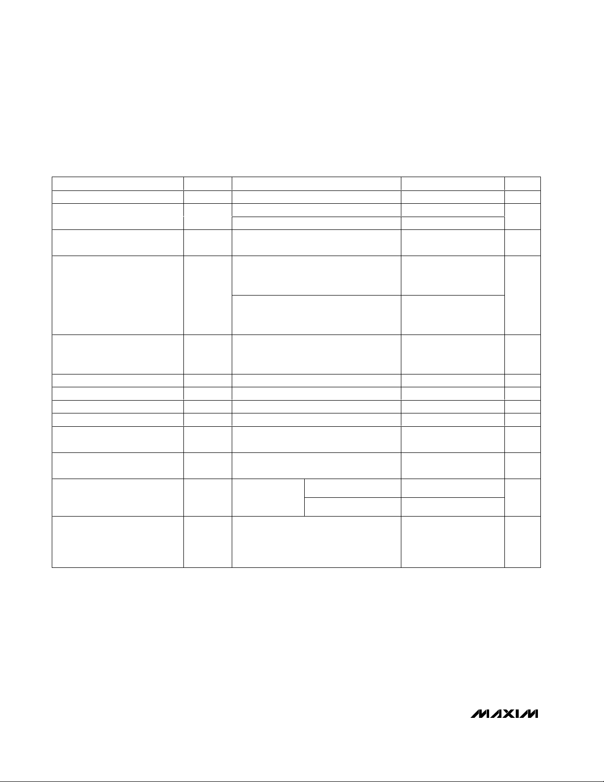
USB
PORT A
USB
PORT B
INPUT
4V TO 5.5V
INA
IN
INB
MAX1823A
FAULTA
FAULTB
ONAONA
ONBONB
OUTA
MAX1823
OUTB
GND
Page 2
MAX1823/MAX1823A/MAX1823B/MAX1823H
Dual USB Switch with Fault
Blanking and Autoreset
2 _______________________________________________________________________________________
ABSOLUTE MAXIMUM RATINGS
Stresses beyond those listed under “Absolute Maximum Ratings” may cause permanent damage to the device. These are stress ratings only, and functional
operation of the device at these or any other conditions beyond those indicated in the operational sections of the specifications is not implied. Exposure to
absolute maximum rating conditions for extended periods may affect device reliability.
IN, INA, INB, ONA, ONB, ONA, ONB
OUTA, OUTB to GND ...........................................-0.3V to +6V
FAULTA, FAULTB to GND..........................-0.3V to (V
IN_
+ 0.3V)
MAX1823/MAX1823H, INA, IN to OUTA;
INB, IN to OUTB ...................................................-0.3V to +6V
MAX1823A/MAX1823B, INA, IN to OUTA;
INB, IN to OUTB (when disabled, Note 3)...............-6V to +6V
INA, IN to OUTA; INB, IN to OUTB
(when enabled, Note 4)..............................-1.5A to +1.5A
RMS
FAULTA, FAULTB Current .................................................20mA
Continuous Power Dissipation (T
A
= +70°C)
10-Pin µMAX (derate 5.6mW/°C above +70°C) ...........444mW
Operating Temperature Range ...........................-40°C to +85°C
Junction Temperature......................................................+150°C
Storage Temperature Range .............................-65°C to +150°C
Lead Temperature (soldering, 10s) .................................+300°C
ELECTRICAL CHARACTERISTICS
(Circuit of Figure 1, VIN= V
INA
= V
INB
= 5V, ONA = ONB = GND (MAX1823/MAX1823A), ONA = ONB = IN (MAX1823B/MAX1823H),
T
A
= 0°C to +85°C, unless otherwise noted. Typical values are at TA= +25°C.)
Supply Voltage Range 4.0 5.5 V
Switch On-Resistance R
Standby Supply Current
PARAMETER SYMBOL CONDITIONS MIN TYP MAX UNITS
TA = +25°C, each switch,
MAX1823/MAX1823H
TA = +25°C, each switch,
MAX1823A/MAX1823B
ON
TA = 0°C to +85°C, each switch,
MAX1823/MAX1823H
TA = 0°C to +85°C, each switch,
MAX1823A/MAX1823B
ON_ = IN_ (MAX1823/MAX1823A), ON_ =
GND (MAX1823B/MAX1823H)
75 105
90 120
135
165
310µA
mΩ
I
= I
Quiescent Supply Current
OUT_ Off-Leakage Current
Undervoltage-Lockout Threshold V
Continuous Load Current 720 mA
Continuous Current Limit I
Short-Circuit Current Limit I
UVLO
LIM
SHORT
OUTA
= I
I
OUTA
ON_ = IN _ ( MAX 1823/M AX1823A), ON _ = GND
(M AX1823B/M AX1823H), V
T
= +25oC
A
ON_ = IN_ (MAX1823/MAX1823A), ON_ =
GND (MAX1823B/MAX1823H),
V
OUTA
Rising edge, 3% hysteresis 3.0 3.4 3.8 V
VIN - V
V
= 0V (I
OUT_
V
= 0V (I
OUT_
= 0A, one channel on 40 80
OUTB
= 0A, both channels on 50 100
OUTB
= V
OUTA
= V
OUT_
= 0V, TA = 0oC to +85oC
OUTB
= 0.5V 0.72 0.90 1.20 A
pulsing) 0.8 1.2 1.6 A
OUT
pulsing) 0.35 A
OUT
OUTB
= 0V,
0.02 1.00
0.02 10.00
µA
µA
PEAK
RMS
Page 3
MAX1823/MAX1823A/MAX1823B/MAX1823H
Dual USB Switch with Fault
Blanking and Autoreset
_______________________________________________________________________________________ 3
ELECTRICAL CHARACTERISTICS (continued)
(Circuit of Figure 1, VIN= V
INA
= V
INB
= 5V, ONA = ONB = GND (MAX1823/MAX1823A), ONA = ONB = IN (MAX1823B/MAX1823H),
T
A
= 0°C to +85°C, unless otherwise noted. Typical values are at TA= +25°C.)
Short-Circuit Detect Threshold (Note 1) 1 V
Continuous Current-Limit
Blanking Timeout Period
Short-Circuit Blanking Timeout
Period
Turn-On Delay t
Output Rise Time t
Turn-Off Delay from ON t
Output Fall Time t
Thermal-Shutdown Threshold 15oC hysteresis +160
Logic Input High Voltage V
Logic Input Low Voltage V
Logic Input Current
FAULT_ Output Low Voltage I
FAULT_ Output High Leakage
Current
Autoreset OUT_ Current In latched-off state, V
Autoreset Threshold In latched-off state, rising 0.4 0.5 0.6 V
Autoreset Blanking Time In latched-off state, V
PARAMETER SYMBOL CONDITIONS MIN TYP MAX UNITS
ON
RISE
OFF
FALL
From continuous current-limit condition to
FAULT_ assertion
From short-circuit current-limit condition to
FAULT_ assertion
R
= 10kΩ,
OUT_
does not include
rise time
R
= 10Ω, from 10% to 90% of V
OUT_
R
_ = 10Ω, does not include fall time (from
OUT
ON_ (MAX1823) or ON_ (MAX1823H)
deasserted to V
R
_ = 10Ω, does not include fall time (from
OUT
ON_ (MAX1823A) or ON_ (MAX1823B)
deasserted to V
R
= 10Ω, from 90% to 10% of V
OUT_
(MAX1823/MAX1823H)
R
= 10Ω, from 90% to 10% of V
OUT_
(MAX1823A/MAX1823B)
= 4V to 5.5V 2 V
IN_
= 4V to 5.5V 0.8 V
IN_
ON_ = GND or IN_ (MAX1823/MAX1823A),
ON_ = GND or IN_ (MAX1823B/MAX1823H)
= 1mA, VIN_ = 4V 0.4 V
SINK
V
_ = V
IN
FAULT_
MAX1823/MAX1823H 0.5 1.2 4.0
MAX1823A/MAX1823B 0.3 0.8 3.0
OUT_
= 90% of V
OUT
= 90% of V
OUT
= 5.5V 1 µA
OUT_
OUT_
)
IN_
)
IN_
OUT_
OUT_
= 0V 10 30 45 mA
> 0.5V 10 20 35 ms
10 20 35 ms
7.5 18 35.0 ms
2.5 ms
0.8 3.0
0.1 3.0
2.5
2.8
-1 +1 µA
ms
ms
ms
o
C
Page 4
MAX1823/MAX1823A/MAX1823B/MAX1823H
Dual USB Switch with Fault
Blanking and Autoreset
4 _______________________________________________________________________________________
ELECTRICAL CHARACTERISTICS
(Circuit of Figure 1, VIN= VIN_ = VON_ = 5V (MAX1823B/MAX1823H); VIN= VIN_ = 5V, ON_ = GND (MAX1823/MAX1823A), TA = -40°C
to +85°C, unless otherwise noted.) (Note 2)
Supply Voltage Range 4.0 5.5 V
Switch On-Resistance R
Standby Supply Current
PARAMETER SYMBOL CONDITIONS MIN TYP MAX UNITS
ON
Each switch, MAX1823/MAX1823H 135
Each switch, MAX1823A/MAX1823B 165
ON_ = IN_ (MAX1823/MAX1823A),
ON_ = GND (MAX1823B/MAX1823H)
I
OUTA
= I
= 0A, one channel on 80
OUTB
10 µA
mΩ
Quiescent Supply Current
= I
I
OUTA
ON_ = IN_ (MAX1823/MAX1823A),
OUT_ Off-Leakage Current
Undervoltage-Lockout Threshold V
Continuous Load Current 720 mA
Continuous Current Limit I
Current Limit into Short Circuit I
Continuous Current-Limit
Blanking Timeout Period
Short-Circuit Blanking Timeout
Period
Turn-On Delay t
Turn-Off Delay from ON t
UVLO
LIM
SHORTVOUT_
ON
OFF
ON_ = GND (MAX1823B/MAX1823H),
V
OUTA
Rising edge, 3% hysteresis 3.0 3.8 V
V
- V
IN_
= 0V (I
From continuous current-limit condition to
FAULT_ assertion
From short-circuit current-limit condition to
FAULT_ assertion
R
= 10kΩ,
OUT_
does not include
rise time
R
OUT_
(from ON_ (MAX1823/MAX1823A) or ON_
(MAX1823B/MAX1823H) deasserted to
V
= 90% V
OUT_
= 0A, both channels on 100
OUTB
= V
OUT_
= 10Ω, does not include fall time
= 0V
OUTB
= 0.5V 0.72 1.20 A
pulsing) 0.8 1.6 A
OUT
10 35 ms
7.5 35.0 ms
MAX1823/MAX1823H 0.5 4.0
MAX1823A/MAX1823B 0.3 3.0
)
IN_
10 µA
3ms
µA
PEAK
ms
Page 5

MAX1823/MAX1823A/MAX1823B/MAX1823H
Dual USB Switch with Fault
Blanking and Autoreset
_______________________________________________________________________________________ 5
ELECTRICAL CHARACTERISTICS (continued)
(Circuit of Figure 1, VIN= VIN_ = VON_ = 5V (MAX1823B/MAX1823H); VIN= VIN_ = 5V, ON_ = GND (MAX1823/MAX1823A), TA = -40°C
to +85°C, unless otherwise noted.) (Note 2)
Note 1: The output voltage at which the device transitions from short-circuit current limit to continuous current limit.
Note 2: Specifications to -40°C are guaranteed by design, not production tested.
Note 3: Reverse current (current from OUT_ to IN_) is blocked when disabled.
Note 4: Forward current (current from IN_ to OUT_) is internally limited. Reverse current, from OUT_ to IN_, is not limited when the
device is enabled and must be kept below 1.5A
RMS
to prevent permanent device damage. When the MAX1823A/MAX1823B
are disabled, the switch turns off and reverse current is internally blocked.
Typical Operating Characteristics
(Circuit of Figure 1, VIN= V
INA
= V
INB
= 5V, ON_ = GND (MAX1823/MAX1823A), ON_ = IN_ (MAX1823B/MAX1823H), TA= +25°C,
unless otherwise noted.)
0
18
12
6
24
30
36
42
48
54
60
021 3456
QUIESCENT CURRENT
vs. INPUT VOLTAGE
MAX1823 toc01
INPUT VOLTAGE (V)
QUIESCENT CURRENT (µA)
45
47
51
49
53
55
-40 10-15 35 60 85
QUIESCENT CURRENT
vs. TEMPERATURE
MAX1823 toc02
TEMPERATURE (°C)
QUIESCENT CURRENT (µA)
VIN_ = 5.5V
VIN_ = 4.5V
VIN_ = 5V
2.5
2.7
3.1
2.9
3.3
3.5
-40 10-15 35 60 85
SHUTDOWN SUPPLY CURRENT
vs. TEMPERATURE
MAX1823 toc03
TEMPERATURE (°C)
SHUTDOWN SUPPLY CURRENT (µA)
ON_ = IN_ (MAX1823/MAX1823A)
ON_ = GND (MAX1823B/MAX1823H)
Logic Input High Voltage V
Logic Input Low Voltage V
Logic Input Current V
FAULT_ Output Low Voltage I
FAULT_ Output High Leakage
Current
Autoreset OUT_Current In latched-off state, V
Autoreset Threshold In latched-off state, rising 0.4 0.6 V
Autoreset Blanking Time In latched-off state, V
PARAMETER SYMBOL CONDITIONS MIN TYP MAX UNITS
= 4V to 5.5V 2 V
IN_
= 4V to 5.5V 0.8 V
IN_
ON_
SINK
V
IN_
= 0V or V
= 1mA, V
= V
IN_
= 4V 0.4 V
IN_
= 5.5V 1 µA
FAULT_
= 0V 10 50 mA
OUT_
> 0.5V 10 35 ms
OUT_
-1 +1 µA
Page 6

MAX1823/MAX1823A/MAX1823B/MAX1823H
Dual USB Switch with Fault
Blanking and Autoreset
6 _______________________________________________________________________________________
Typical Operating Characteristics (continued)
(Circuit of Figure 1, VIN= V
INA
= V
INB
= 5V, ON_ = GND (MAX1823/MAX1823A), ON_ = IN_ (MAX1823B/MAX1823H), TA= +25°C,
unless otherwise noted.)
SWITCH OFF-LEAKAGE
vs. TEMPERATURE
1000
NORMALIZED RON vs. TEMPERATURE
1.50
CONTINUOUS CURRENT-LIMIT
THRESHOLD vs. TEMPERATURE
940
RISE
MAX1823 toc04
1.25
ON
1.00
NORMALIZED R
0.75
0.50
-40 10-15 35 60 85
TEMPERATURE (°C)
TURN-OFF TIME
)
MAX1823 toc07
vs. TEMPERATURE (t
3.5
3.3
VIN_ = 5V
3.1
2.9
TURN-OFF TIME (ms)
2.7
VIN_ = 4.5V
2.5
-40 10-15 35 60 85
TEMPERATURE (°C)
+ t
OFF
VIN_ = 5.5V
AUTORESET CURRENT vs. TEMPERATURE
(MAX1823/MAX1823H)
40
MAX1823 toc10
35
30
25
AUTORESET CURRENT (mA)
20
15
-40 10-15 35 60 85
VIN_ = 4.5V
TEMPERATURE (°C)
VIN_ = 5.5V
VIN_ = 5V
100
10
1
SWITCH OFF-LEAKAGE (nA)
0.1
0.01
-40 10-15 35 60 85
TEMPERATURE (°C)
TURN-ON TIME
vs. TEMPERATURE (t
4.0
3.8
3.6
3.4
TURN-ON TIME (ms)
3.2
3.0
VIN_ = 4.5V
VIN_ = 5.5V
-40 10-15 35 60 85
TEMPERATURE (°C)
+ t
ON
VIN_ = 5V
FAULT_ OUTPUT LOW VOLTAGE
vs. TEMPERATURE
0.250
I
_ = 1mA
FAULT
0.225
0.200
0.175
0.150
FAULT_ OUTPUT LOW VOLTAGE (V)
0.125
0.100
VIN_ = 4.5V
-40 10-15 35 60 85
TEMPERATURE (°C)
VIN_ = 5V
VIN_ = 5.5V
FALL
)
MAX 1823 toc05
MAX1823 toc08
V
=
IN_
930
920
V
=
IN_
V
=
IN_
910
CONTINUOUS CURRENT LIMIT (mA)
900
-40 10-15 35 60 85
22.0
21.8
21.6
21.4
FAULT-BLANKING TIME (ms)
21.2
21.0
VIN_ = 4.5V
-40 10-15 35 60 85
AUTORESET CURRENT vs. TEMPERATURE
36
MAX1823 toc11
34
32
30
AUTORESET CURRENT (mA)
VIN_ = 4.5V
28
-40 10-15 35 60 85
5.5V
5V
4.5V
TEMPERATURE (°C)
FAULT-BLANKING TIME
vs. TEMPERATURE
VIN_ = 5.5V
TEMPERATURE (°C)
(MAX1823A/MAX1823B)
VIN_ = 5.5V
VIN_ = 5V
TEMPERATURE (°C)
MAX1823 toc06
MAX1823 toc09
VIN_ = 5V
MAX1823 toc12
Page 7

MAX1823/MAX1823A/MAX1823B/MAX1823H
Dual USB Switch with Fault
Blanking and Autoreset
_______________________________________________________________________________________ 7
Typical Operating Characteristics (continued)
(Circuit of Figure 1, VIN= V
INA
= V
INB
= 5V, ON_ = GND (MAX1823/MAX1823A), ON_ = IN_ (MAX1823B/MAX1823H), TA= +25°C,
unless otherwise noted.)
AUTORESET CURRENT vs. INPUT VOLTAGE
(MAX1823/MAX1823H)
50
40
30
20
AUTORESET CURRENT (mA)
10
0
3.6 5.24.4 6.0
TA = +25°C
INPUT VOLTAGE (V)
OVERLOAD RESPONSE INTO 2.5Ω
(MAX1823A/MAX1823B ONLY)
A
B
C
D
TA = -40°C
TA = +85°C
OVERLOAD RESPONSE INTO 2.5Ω
(MAX1823/MAX1823H)
A
B
C
D
10ms/div
, 5V/div
C: V
D: I
FAULTA
OUTA
, 1A/div
A: V
B: V
IN_
OUTA
, 5V/div
SHORT-CIRCUIT RESPONSE INTO 0Ω
(MAX1823/MAX1823H)
A
B
C
D
, 5V/div
MAX1823 toc16
AUTORESET CURRENT vs. INPUT VOLTAGE
39
MAX1823 toc13
5V
0
0
0
37
35
33
31
29
AUTORESET CURRENT (mA)
27
25
A
B
C
D
(MAX1823A/MAX1823B)
TA = +85°C
TA = +25°C
TA = -40°C
3.6 5.24.4 6.0
INPUT VOLTAGE (V)
OVERLOAD RESPONSE INTO 2.5Ω
(EXPANDED TIME SCALE)
MAX1823 toc17
MAX1823 toc14
5V
0
0
0
MAX1823 toc15
5V
0
0
0
MAX1823 toc18
5V
0
0
0
10ms/div
, 5V/div
C: V
D: I
FAULTA
OUTA
, 1A/div
A: V
B: V
IN_
OUTA
, 5V/div
SHORT-CIRCUIT RESPONSE INTO 0Ω
(MAX1823A/MAX1823B)
A
B
C
D
, 5V/div
10ms/div
C: V
D: I
FAULTA
OUTA
A: VIN_, 5V/div
B: V
OUTA
, 5V/div
, 5V/div
, 2A/div
MAX1823 toc19
500
A: V
B: V
IN_
OUTA
, 5V/div
, 5V/div
C: V
D: I
µs/div
FAULTA
OUTA
, 5V/div
, 1A/div
A: VIN_, 5V/div
B: V
OUTA
SHORT-CIRCUIT RESPONSE INTO 0Ω
(EXPANDED TIME SCALE)
A
5V
B
0
C
0
D
0
, 5V/div
500µs/div
C: V
D: I
A: V
B: V
IN_
OUTA
, 5V/div
FAULTA
OUTA
, 5V/div
, 2A/div
MAX1823 toc20
5V
A
0
5V
B
0
A: V
, 5V/div
ONA
B: V
OUTA
10ms/div
, 5V/div
C: V
D: I
FAULTA
OUTA
, 5V/div
, 1A/div
SWITCH TURN-ON TIME
(MAX1823/MAX1823A)
1ms/div
, 2V/div
MAX1823 toc21
0
0
Page 8

MAX1823/MAX1823A/MAX1823B/MAX1823H
Dual USB Switch with Fault
Blanking and Autoreset
8 _______________________________________________________________________________________
Pin Description
Typical Operating Characteristics (continued)
(Circuit of Figure 1, VIN= V
INA
= V
INB
= 5V, ON_ = GND (MAX1823/MAX1823A), ON_ = IN_ (MAX1823B/MAX1823H), TA= +25°C,
unless otherwise noted.)
*() are for the MAX1823B/MAX1823H only.
SWITCH TURN-OFF TIME
A
+ t
(t
OFF
)
FALL
MAX1823 toc22
0
STARTUP TIME
(TYPICAL USB APPLICATION)
A
B
MAX1823 toc23
0
5V
C
B
0
1ms/div
A: V
, 5V/div
ONA
, 2V/div
B: V
OUTA
PIN NAME FUNCTION
1
2, 3, 4
5
*(ONA)
INA, IN,
*(ONB)
6 FAULTB
7 OUTB
ONA
INB
ONB
C ontr ol Inp ut for S w i tch A. C an b e d r i ven hi g her than IN_ w i thout d am ag e. A l og i c l ow tur ns sw i tch A on for
the M AX 1823/M AX 1823A, and a l og i c hi g h tur ns sw i tch A on for the M AX 1823B/M AX 1823H .
Power Input. Connect all IN_ pins together, and bypass with a 0.1µF capacitor to ground. Load
conditions may require additional bulk capacitance to prevent the input from being pulled down.
Control Input for Switch B. Can be driven higher than IN_ without damage. A logic low turns switch B
on for the M AX 1823/M AX 1823A, and a logic high turns switch B on for the M AX 1823B/M AX 1823H .
Fault-Indicator Output for Switch B. This open-drain output goes low when switch B is in thermal
shutdown or UVLO or in a sustained (>20ms) current-limit or short-circuit condition.
Power Output for Switch B. Connect a 1µF capacitor from OUTB to ground. Load condition may
require additional bulk capacitance.
D
, 5V/div
, 5V/div
500µs/div
C: V
D : I
OUTA
OUTA
, 2V/div
, 0.5A/div
A: V
B: V
ONA
FAULTA
8 GND Ground
9 OUTA
10 FAULTA
Power Output for Switch A. Connect a 1µF capacitor from OUTA to ground. Load condition may
require additional bulk capacitance.
Fault-Indicator Output for Switch A. This open-drain output goes low when switch A is in thermal
shutdown or UVLO or in a sustained (>20ms) current-limit or short-circuit condition.
0
0
Page 9

MAX1823/MAX1823A/MAX1823B/MAX1823H
Dual USB Switch with Fault
Blanking and Autoreset
_______________________________________________________________________________________ 9
Detailed Description
The MAX1823 is a dual, current-limited switch designed
for USB applications. It has two independent switches,
each with its own enable control input and autoreset
function. Each switch has an error-flag output to notify
the USB controller when the current-limit, short-circuit,
undervoltage-lockout, or thermal-shutdown threshold is
reached (Figure 2).
The MAX1823 operates from a 4V to 5.5V input voltage
range and guarantees a minimum 720mA output current.
A built-in 0.9A current limit limits the current in the event
of a heavy-overload condition. The MAX1823 has independent thermal shutdown for each switch in the event
of a prolonged overload or short-circuit condition. The
autoreset function monitors the overload and automatically turns the switch on when the overload is removed.
Use of low-RONNMOS switches enables the MAX1823
to provide two switches in the ultra-small 10-pin µMAX
package. An internal micropower charge pump generates the high-side supply needed for driving the gates
of these high-side switches. Separate current-limiting
and thermal-shutdown circuits permit each switch to
operate independently, improving system robustness.
Undervoltage-Lockout and
Input-Voltage Requirements
The MAX1823 includes a UVLO circuit to prevent erroneous switch operation when the input voltage goes
low during startup and brownout conditions. Operation
is inhibited when V
IN_
is less than 3.4V.
Output Fault Protection
The MAX1823 senses the switch output voltage and
selects continuous current limiting when V
OUT
is greater
than 1V or short-circuit current limiting when V
OUT
is less
than 1V. When V
OUT
is greater than 1V, the device operates in a continuous current-limit mode that sets the output current limit to 0.9A. When V
OUT
is less than 1V, the
device operates in short-circuit current-limit mode,
sourcing 0.35A
RMS
current pulses to the load.
Autoreset Mode
If an output fault is detected for more than the 20ms
blanking time, the output latches off, the FAULT_ output
goes low, and a 25mA current is forced at the output. If
the voltage on the output exceeds 0.5V for 20ms, the fault
resets, the 25mA current source shuts down, and the output turns on. The device monitors the output voltage so
that a short-circuit condition can be detected. Active
loads are not expected to have measurable currents
when the supply is below 0.5V. The MAX1823/MAX1823A
can also be reset from fault manually by toggling ON_
(ON_ for the MAX1823B/MAX1823H) for that channel.
Thermal Shutdown
The MAX1823 features independent thermal shutdown
for each switch channel, allowing one switch to deliver
power even if the other switch has a fault condition.
When the junction temperature exceeds +160°C, the
switch turns off and the FAULT_ output goes low immediately; fault blanking does not occur during thermal
limit. When the junction cools by 15°C, the switch turns
on again. If the fault overload condition continues, the
switch cycles on and off, resulting in a pulsed output,
saving battery power.
Reverse Current Blocking
The USB specification does not allow an output device
to source current back into the USB port. However, the
MAX1823A/MAX1823B are designed to safely power
noncompliant devices. When disabled, each output is
switched to a high-impedance state, blocking reverse
current flow from the output back to the input. However,
during normal operation with the device enabled, the
MAX1823A/MAX1823B are bidirectional switches.
Fault Indicators
The MAX1823 provides an open-drain fault output
(FAULT_) for each switch. For most applications, connect
FAULT_ to IN_ through a 100kΩ pullup resistor. FAULT_
goes low when any of the following conditions occur:
• The input voltage is below the UVLO threshold.
• The switch junction temperature exceeds the
+160°C thermal-shutdown temperature limit.
• The switch is in current-limit or short-circuit limit
mode after the fault-blanking period is exceeded.
• The switch is in autoreset mode.
Figure 1. Typical Application Circuit
INA
INPUT
4V TO 5.5V
* USB APPLICATIONS MAY REQUIRE
ADDITIONAL BULK CAPACITANCE.
0.1µF
100kΩ
100kΩ
IN
INB
FAULTA
FAULTB
ONAONA
ONBONB
OUTA
MAX1823
OUTB
GND
USB
PORT A
1µF*
USB
PORT B
1µF*
Page 10

MAX1823/MAX1823A/MAX1823B/MAX1823H
Dual USB Switch with Fault
Blanking and Autoreset
10 ______________________________________________________________________________________
After the fault condition is removed, the FAULT_ output
deasserts after a 20ms delay. Ensure that the MAX1823
has adequate input bypass capacitance to prevent
glitches from triggering FAULT_ outputs. Input glitches
greater than 0.2V/µs may cause erroneous FAULT_
indications.
Behavior During Current Limit
and Fault Blanking
The MAX1823 limits switch current in three ways. When
ON_ is deasserted (high for MAX1823/MAX1823A, low
for MAX1823B/MAX1823H), the switch is off and leakage dominates the residual output current. When ON_
is asserted (low for MAX1823/MAX1823A, high for
MAX1823B/MAX1823H), the switch supplies a continuous output current of at least 720mA. When the output
current exceeds the 0.9A threshold, the MAX1823 limits the current depending on the output voltage. For
V
OUT_
greater than 1V (current-limit mode), the
MAX1823 regulates the output current to 0.9A. For
V
OUT_
less than 1V (short-circuit mode), the MAX1823
pulses the switch, decreasing the current to 0.35A
RMS
(Table 1). Note that a thermal overload may result from
either of these high-current conditions.
The MAX1823 switches may enter current limit in normal operation when powering up or driving heavy
capacitive loads. To differentiate these conditions from
short circuits or sustained overloads that may damage
the device, the MAX1823 has an independent faultblanking circuit in each switch. When a load transient
causes the device to enter current limit, an internal
counter starts to monitor the duration of the fault. For
load faults exceeding 20ms fault-blanking time, the
switch turns off, the FAULT_ signal asserts low, and the
device enters autoreset mode (see the Autoreset Mode
section). Only current-limit and short-circuit faults are
blanked. Thermal-overload faults and input voltage
drops below the UVLO threshold immediately cause
the switch to turn off and FAULT_ to assert low.
Figure 2. Functional Diagram
INA
ONA
*(ONA)
CHARGE
PUMP
INA
FAULTA
BIAS
UVLO
REF
4V TO 5.5V
IN_
0.1µF
*(ONB)
ONB
INB
*( ) ARE FOR THE MAX1823B/MAX1823H.
MAX1823B/MAX1823H
OSC
25kHz
MAX1823/MAX1823A
CHARGE
PUMP
THERMAL
SHUTDOWN
TIMER
20ms
ILIM
25mA
FAULT
LOGIC
25mA
ILIM
FAULTB
OUTA
1µF
GND
OUTB
1µF
INB
Page 11

MAX1823/MAX1823A/MAX1823B/MAX1823H
Dual USB Switch with Fault
Blanking and Autoreset
______________________________________________________________________________________ 11
Table 1. MAX1823 Current Limiting and Fault Behavior
Fault blanking allows the MAX1823 to handle USB loads
that may not be fully compliant with the USB specifications. USB loads with additional bypass capacitance
and/or large startup currents can be successfully powered even while protecting the upstream power source.
No fault is indicated if the switch is able to bring up the
load within the 20ms blanking period.
Applications Information
Input Power Source
IN, INA, and INB provide the power for all control and
charge-pump circuitry. All three IN_ pins must be connected together externally. The input-voltage slew rate
should be less than 0.2V/µs to prevent erroneous
FAULT_ indications. This condition should not occur
under normal USB applications.
Input Capacitor
Connect a capacitor from IN_ to ground to limit the input
voltage drop during momentary output short-circuit conditions. A 0.1µF ceramic capacitor is required for local
decoupling; higher capacitor values further reduce the
voltage drop at the input (see the Typical Application
Circuit (Figure 1)). When driving inductive loads, a larger capacitance prevents voltage spikes from exceeding
the MAX1823’s absolute maximum ratings.
Output Capacitor
Place a 1µF or greater capacitor at each output for noise
immunity. When starting up into very large capacitive
loads, the switch pulses the output current at 0.35A
RMS
until the output voltage rises above 1V, then the capacitor
continues to charge at the full 0.9A current limit. There is
no limit to the output capacitor size, but to prevent a startup fault assertion, the capacitor must charge up within
the fault-blanking delay period. Typically, starting up into
a 330µF or smaller capacitor does not trigger a fault output. In addition to bulk capacitance, small-value (0.1µF or
greater) ceramic capacitors improve the output’s
resilience to electrostatic discharge (ESD).
Driving Inductive Loads
A wide variety of devices (mice, keyboards, cameras,
and printers) can load the USB port. These devices commonly connect to the port with cables, which can add an
inductive component to the load. This inductance causes
the output voltage at the USB port to ring during a load
step. The MAX1823 is capable of driving inductive loads,
but avoids exceeding the device’s absolute maximum ratings. Usually the load inductance is relatively small, and
the MAX1823’s input includes a substantial bulk capacitance from an upstream regulator as well as local bypass
capacitors, limiting overshoot. If severe ringing occurs
due to large load inductance, clamp the MAX1823’s output below 6V and above -0.3V.
CONDITION MAX1823 BEHAVIOR
• An output short circuit ramps the current to I
blanking timer turns on, FAULT_ stays high, and the output current pulses at 0.35A
Output short circuit
< 1V)
(V
OUT
Output overload current
> 1V)
(V
OUT
Thermal fault
(T
> +160°C)
J
• Removing the short circuit before the 15ms short-circuit blanking timeout period allows the
next ramped current pulse to soft-start the output. The FAULT_ flag stays high.
• A short circuit exceeding 15ms to 20ms forces FAULT_ low at 20ms, enables autoreset
mode, and sources 25mA at the output.
• An output voltage above 0.5V for 20ms resets the switch, turns on the output, and forces
FAULT_ high.
• An output overload regulates the current at I
overload is removed, a thermal fault occurs, or the 20ms continuous current-limit timeout
period is reached.
• An overcurrent condition still present at 20ms forces FAULT_ low, enables autoreset, and
sources 25mA at the output.
• An output voltage above 0.5V for 20ms resets the switch, turns on the output, and forces
FAULT_ high.
• A junction temperature of +160°C immediately forces FAULT_ low (the blanking timer does
not apply to thermal faults) and turns off the switch. The junction cooling 15°C removes the
thermal fault condition, enables autoreset mode, and sources 25mA at the output. FAULT_
remains low while a thermal fault condition is present.
• An output voltage above 0.5V for 20ms resets the switch, turns on the output, and forces
FAULT_ high.
in 2ms to 3ms, the switch shuts off, the
SHORT
(0.9A), and FAULT_ stays high until the
LIM
RMS
.
Page 12

MAX1823/MAX1823A/MAX1823B/MAX1823H
Dual USB Switch with Fault
Blanking and Autoreset
12 ______________________________________________________________________________________
Turn-On and Turn-Off Behavior
In the absence of faults, the MAX1823’s internal switches
turn on and off slowly under the control of the ON_
inputs. Transition times for both edges are provided in
the Electrical Characteristics table. The slow chargepump switch drive minimizes load transients on the
upstream power source. Under thermal fault and UVLO,
the power device turns off rapidly (100ns) to protect the
power device.
Layout and Thermal Dissipation
To optimize the switch response time to output shortcircuit conditions, keep all traces as short as possible
to reduce the effect of undesirable parasitic inductance. Place input and output capacitors no more than
5mm from device leads. All IN_ and OUT_ pins must be
connected with short traces to the power bus. Wide
power-bus planes provide superior heat dissipation
through the switch IN_ and OUT_ pins.
While the switches are on, power dissipation is small, and
the package temperature change is minimal. Calculate
the power dissipation for this condition as follows:
P = (I
OUT_
)2R
ON
For the normal operating current (I
OUT_
= 0.5A), and
the maximum on-resistance of the switch (135mΩ), the
power dissipation is:
P = (0.5A)2x 0.135Ω = 34mW per switch
The worst-case power dissipation occurs when the
switch is in current limit and the output is greater than
1V. In this case, the power dissipated in each switch is
the voltage drop across the switch multiplied by the
current limit:
P = (I
LIM
) (VIN- V
OUT
)
For a 5V input and 1V output, the maximum power dissipation per switch is:
P = (1.2A) ( 5V - 1V) = 4.8W
Since the package power dissipation is only 444mW,
the MAX1823 die temperature exceeds the thermalshutdown threshold, and the switch output shuts down
until the junction temperature cools by 15°C. The duty
cycle and period are strong functions of the ambient
temperature and the PC board layout.
A short circuit at the output causes the power dissipated
across the switch and the junction temperature to
increase. If the fault condition persists, the thermaloverload-protection circuitry activates, and the output
shuts down until the junction temperature decreases by
15°C (see the Thermal Shutdown section).
Since the output short-circuit current is 25mA (typ), and
with V
IN_
= 5V, calculate the power dissipation for a
short-circuited output as follows:
P = (0.025A)(5) = 0.125W
Chip Information
TRANSISTOR COUNT: 3227
PROCESS: BiCMOS
Page 13

MAX1823/MAX1823A/MAX1823B/MAX1823H
Dual USB Switch with Fault
Blanking and Autoreset
Maxim cannot assume responsibility for use of any circuitry other than circuitry entirely embodied in a Maxim product. No circuit patent licenses are
implied. Maxim reserves the right to change the circuitry and specifications without notice at any time.
Maxim Integrated Products, 120 San Gabriel Drive, Sunnyvale, CA 94086 408-737-7600 ____________________ 13
© 2003 Maxim Integrated Products Printed USA is a registered trademark of Maxim Integrated Products.
Package Information
(The package drawing(s) in this data sheet may not reflect the most current specifications. For the latest package outline information,
go to www.maxim-ic.com/packages.)
0.6±0.1
e
10
ÿ 0.50±0.1
1
0.6±0.1
TOP VIEW
D2
A2
b
D1
FRONT VIEW
4X S
10
DIM
H
1
BOTTOM VIEW
E2
GAGE PLANE
A
A1
α
E1
L
L1
INCHES
MIN
-A
0.002
A1
A2 0.030 0.037 0.75 0.95
0.116
D1
0.114
D2
0.116
E1
0.114
E2
0.187
H
0.0157
L
L1
0.037 REF
0.007
b
e
0.0197 BSC
0.0035
c
0.0196 REF
S
α
0∞ 0∞ 6∞
c
MAX
0.043
0.006
0.120
0.118
0.120
0.118
0.199
0.0275
0.0106
0.0078
6∞
MILLIMETERS
MAX
MIN
1.10
-
0.15
0.05
3.05
2.95
3.00
2.89
3.05
2.95
2.89
3.00
4.75
5.05
0.40
0.70
0.940 REF
0.177
0.270
0.500 BSC
0.090
0.200
0.498 REF
10LUMAX.EPS
SIDE VIEW
PROPRIETARY INFORMATION
TITLE:
PACKAGE OUTLINE, 10L uMAX/uSOP
REV.DOCUMENT CONTROL NO.APPROVAL
21-0061
1
I
1
 Loading...