

Page 1
For price, delivery, and to place orders, please contact Maxim Distribution at 1-888-629-4642,
or visit Maxim’s website at www.maxim-ic.com.
General Description
The MAX1812 is a dual current-limited switch specifically made for USB applications. Each channel is guaranteed to supply 500mA and meets USB specifications.
The MAX1812’s low quiescent supply current (45µA)
and shutdown current (3µA) conserve battery power in
portable applications.
The MAX1812 has multiple safety features to ensure
that the USB port is protected. Built-in thermal-overload
protection limits power dissipation and junction temperature. The device also has accurate internal current-limiting circuitry to protect the input supply against both
overload and short-circuit conditions. Independent fault
signals (FAULTA and FAULTB) notify the microprocessor when a thermal-overload, current limit, undervoltage
lockout, or short-circuit fault occurs. A 20ms fault-blanking feature enables the circuit to ignore momentary
faults, such as those caused when hot-swapping a
capacitive load, thereby preventing false alarms to the
host system.
The MAX1812 is available in a space-saving 10-pin
µMAX package. For single versions of this device, refer
to the MAX1693, MAX1694, and MAX1607 data sheets.
________________________Applications
USB Ports
USB Hubs
Notebook Computers
Desktop Computers
PDAs and Palmtop Computers
Docking Stations
Features
♦ Dual USB Switch in Tiny 10-Pin µMAX Package
♦ Guaranteed 500mA Load per Channel
♦ Built-In 20ms Fault Blanking
♦ Compliant to USB Specifications
♦ +4.0V to +5.5V Input Voltage Range
♦ 45µA Quiescent Current
♦ 3µA Shutdown Current
♦ Independent Shutdown Control
♦ Independent FAULT Indicator Outputs
♦ Thermal-Overload Protection
♦ UL Listing Pending
MAX1812
Dual USB Switch with Fault Blanking
________________________________________________________________ Maxim Integrated Products 1
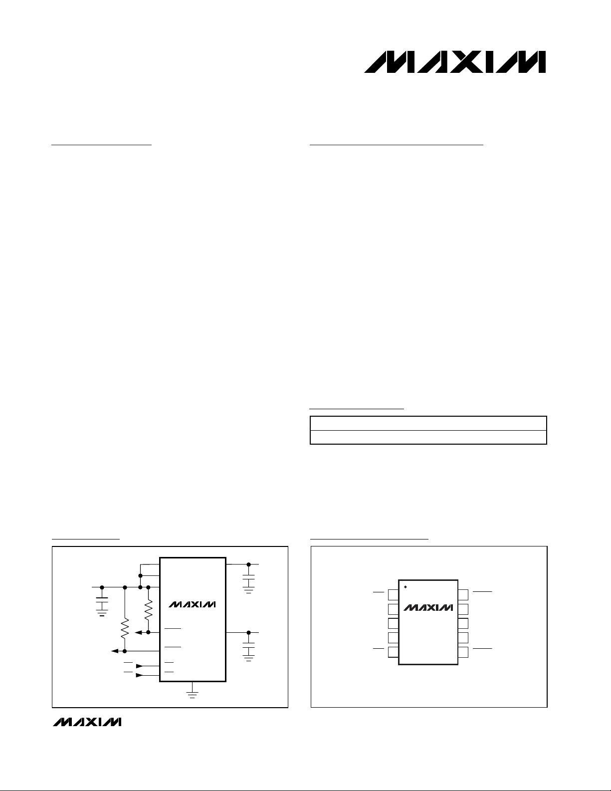
Pin Configuration
ONBONB
ONAONA
GND
MAX1812
FAULTB
FAULTA
IN
INA
INB
USB
PORT A
OUTA
USB
PORT B
OUTB
INPUT
4.0V TO 5.5V
Typical Operating Circuit
19-1865; Rev 0; 11/00
1
2
3
4
5
10
9
8
7
6
OUTA
GND
OUTBINB
IN
INA
MAX1812
µMAX
TOP VIEW
ONA
ONB FAULTB
FAULTA
Ordering Information
PART TEMP. RANGE PIN-PACKAGE
MAX1812EUB -40°C to +85°C 10 µMAX
Page 2
MAX1812
Dual USB Switch with Fault Blanking
2 _______________________________________________________________________________________
ABSOLUTE MAXIMUM RATINGS
ELECTRICAL CHARACTERISTICS
(VIN= V
INA
= V
INB
= 5V, TA= -40°C to +85°C, unless otherwise noted. Typical values are at TA= +25°C) (Note 1)
Stresses beyond those listed under “Absolute Maximum Ratings” may cause permanent damage to the device. These are stress ratings only, and functional
operation of the device at these or any other conditions beyond those indicated in the operational sections of the specifications is not implied. Exposure to
absolute maximum rating conditions for extended periods may affect device reliability.
IN, INA, INB, ONA, ONB, OUTA, OUTB to GND......-0.3V to +6V
FAULTA, FAULTB to GND .........................-0.3V to (V
IN
_ + 0.3V)
INA, IN to OUTA; INB, IN to OUTB..........................-0.3V to +6V
OUTA, OUTB Maximum Continuous Switch Current
(per channel, internally limited) .........................................1.2A
FAULTA, FAULTB Current .................................................20mA
Continuous Power Dissipation (T
A
= +70°C)
10-Pin µMAX (derate 5.6mW/°C above +70°C) ............444mW
Operating Temperature Range ...........................-40°C to +85°C
Junction Temperature......................................................+150°C
Storage Temperature Range .............................-65°C to +150°C
Lead Temperature (soldering, 10s) .................................+300°C
Supply Voltage Range 4.0 5.5 V
Switch On-Resistance R
Standby Supply Current Both switches disabled 3 10 µA
Quiescent Supply Current Both switches enabled, I
OUT_ Leakage Current
U nd er vol tag e Lockout Thr eshol d UVLO Rising edge, 3% hysteresis 3.0 3.4 3.8 V
Continuous Load Current 500 mA
Continuous Current Limit ILIM VIN_ - V
Short-Circuit Current Limit ISHORT V
Short-Circuit Detect Threshold (Note 2) 1 V
Continuous Current-Limit
Blanking Timeout Period
Short-Circuit Blanking Timeout
Period
Turn-On Delay
Output Rise Time
Turn-Off Delay from ON
Output Fall Time
Thermal Shutdown Threshold 15°C hysteresis 160 °C
PARAMETER SYMBOL CONDITIONS MIN TYP MAX UNITS
ON
TA = +25°C, each switch 75 105
TA = -40°C to +85°C, each switch 135
Switches disabled, V
T
= +25°C
A
Switches disabled, V
T
= -40°C to 85°C
A
_ = 0.5V 0.6 0.9 1.2 A
OUT
OUT
_ = 0 (I
OUT
pulsing)
OUTA
OUTA
OUTA
= V
= V
= I
OUTB
OUTB
= 0 45 100 µA
OUTB
= 0,
= 0,
From continuous current-limit condition to
FAULT_ assertion
From short-circuit current-limit condition to
FAULT_ assertion
R
= 10Ω, C
OUT
rise time (from ON_ to 10% of V
R
= 10Ω, C
OUT
90% of V
R
OUT
OUT
= 10Ω, C
fall time (from ON_ to 90% of V
C
= 1µF, R
OUT
of V
OUT
= 1µF does not include
OUT
OUT
= 1µF, from 10% to
OUT
= 1µF does not include
OUT
OUT
= 10Ω, from 90% to 10%
OUT
)
)
0.002 1
10
0.8 1.2 1.6 A( peak)
0.35 A
10 20 35 ms
7.5 18 35 ms
0.5 1.2 4.0 ms
2.5 ms
0.8 3 ms
2.5 ms
mΩ
µA
RMS
Page 3
MAX1812
Dual USB Switch with Fault Blanking
_______________________________________________________________________________________ 3
ELECTRICAL CHARACTERISTICS (continued)
(VIN= V
INA
= V
INB
= 5V, TA= -40°C to +85°C, unless otherwise noted. Typical values are at TA= +25°C.) (Note 1)
Note 1: Specifications to -40°C are guaranteed by design, not production tested.
Note 2: The output voltage at which the device transitions from short-circuit current limit to continuous current limit.
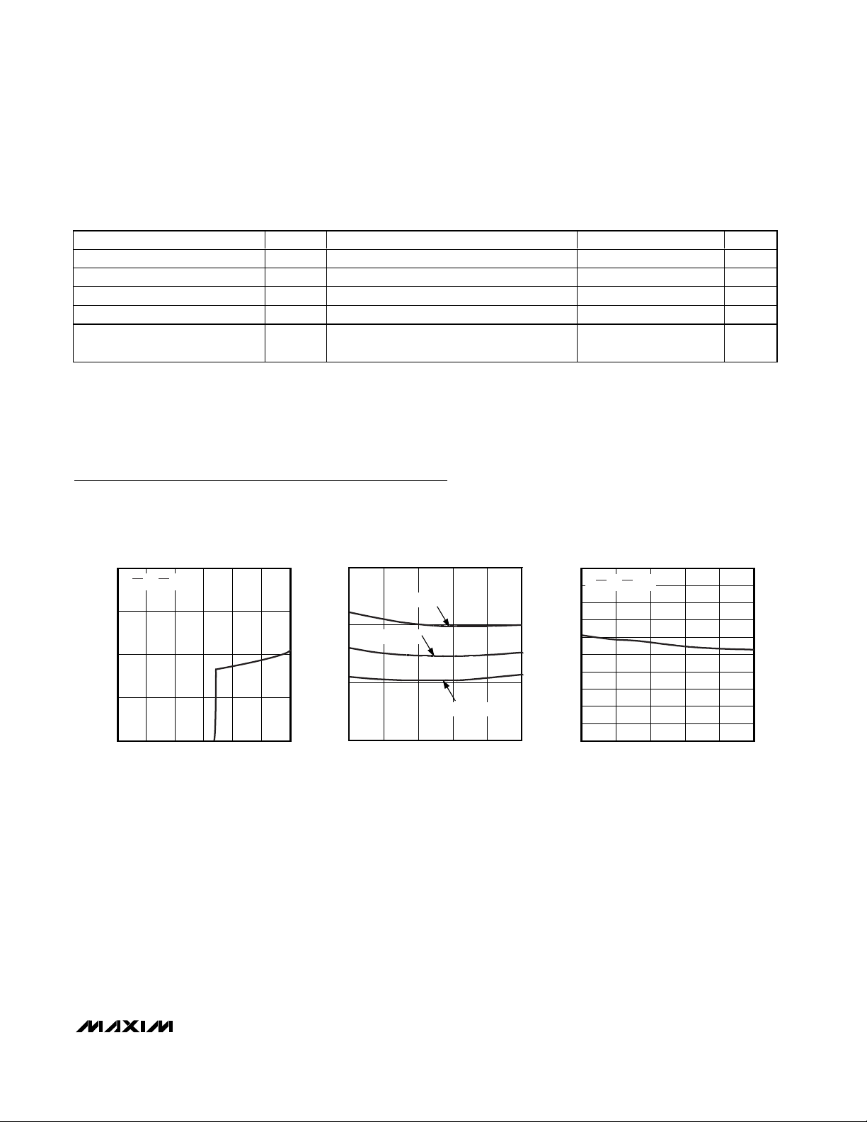
Typical Operating Characteristics
(VIN= V
INA
= V
INB
= 5V, Circuit of Figure 2, TA = +25°C, unless otherwise noted.)
100
75
50
25
0
0312 456
QUIESCENT CURRENT
vs. INPUT VOLTAGE
MAX1812 toc01
INPUT VOLTAGE (V)
QUIESCENT CURRENT (µA)
V
ONA
= V
ONB
= 0V
40
45
50
55
-40 10-15 35 60 85
QUIESCENT CURRENT
vs. TEMPERATURE
MAX1812 toc02
TEMPERATURE (°C)
QUIESCENT CURRENT (µA)
VIN = 4.5V
VIN = 5V
VIN = 5.5V
0
1
2
3
4
5
-40 10-15 35 60 85
SHUTDOWN SUPPLY CURRENT
vs. TEMPERATURE
MAX1812 toc03
TEMPERATURE (°C)
SHUTDOWN SUPPLY CURRENT (µA)
V
ONA
= V
ONB
= V
IN
Logic Input High Voltage V
Logic Input Low Voltage V
Logic Input Current V
FAULT_ Output Low Voltage I
FAULT_ Output High Leakage
Current
PARAMETER SYMBOL CONDITIONS MIN TYP MAX UNITS
= +4V to +5.5V 2 V
IN_
= +4V to +5.5V 0.8 V
IN_
SINK
V
ON_
IN_
= 0 or V
= 1mA, V
= V
FAULT_
IN_
= 4V 0.4 V
IN_
= 5.5V 1 µA
-1 1 µA
Page 4

MAX1812
Dual USB Switch with Fault Blanking
4 _______________________________________________________________________________________
Typical Operating Characteristics
(VIN= V
INA
= V
INB
= 5V, Circuit of Figure 2, TA = +25°C, unless otherwise noted.)
1.50
1.25
1.00
0.75
0.50
-40 10-15 35 60 85
NORMALIZED RON vs. TEMPERATURE
MAX 1812 toc05
TEMPERATURE (°C)
NORMALIZED R
ON
V
ONA
= V
ONB
= 0V
800
830
820
810
840
850
860
870
880
890
900
-40 10-15 35 60 85
CONTINUOUS CURRENT LIMIT
vs. TEMPERATURE
MAX1812 toc06
TEMPERATURE (°C)
CONTINUOUS CURRENT LIMIT (mA)
VIN = 5V
2.6
2.9
2.8
2.7
3.0
3.1
3.2
3.3
3.4
3.5
3.6
-40 10-15 35 60 85
TOTAL TURN-OFF TIME
vs. TEMPERATURE
MAX1812 toc08
TEMPERATURE (°C)
TOTAL TURN-OFF TIME (ms)
VIN = 5.5V
VIN = 5V
VIN = 4.5V
TOTAL TURN-OFF
TIME = FALL TIME + DELAY TIME
22.0
21.5
21.0
20.5
20.0
-40 10-15 35 60 85
FAULT-BLANKING TIME
vs. TEMPERATURE
MAX1812 toc09
TEMPERATURE (°C)
FAULT-BLANKING TIME (ms)
VIN = 5.0V
1000
0.1
-40 10-15 60
OUT_ LEAKAGE CURRENT
vs. TEMPERATURE
1
10
100
MAX1812 toc04
TEMPERATURE (°C)
LEAKAGE CURRENT (nA)
35 85
V
ONA
= V
ONB
= V
IN
3.0
3.3
3.2
3.1
3.4
3.5
3.6
3.7
3.8
3.9
4.0
-40 10-15 35 60 85
TOTAL TURN-ON TIME
vs. TEMPERATURE
MAX1812 toc07
TEMPERATURE (°C)
TOTAL TURN-ON TIME (ms)
V
IN
= 4.5V
V
IN
= 5V
V
IN
= 5.5V
TOTAL TURN-ON
TIME = RISE TIME + DELAY TIME
0.100
0.150
0.125
0.200
0.175
0.225
0.250
-40 10-15 35 60 85
FAULT OUTPUT LOW VOLTAGE
vs. TEMPERATURE
MAX1812 toc10
TEMPERATURE (°C)
FAULT OUTPUT LOW VOLTAGE (V)
VIN = 4.5V
VIN = 5V
VIN = 5.5V
5ms/div
A
B
D
C
0
5V
0
0
MAX1812-11
A : V
IN,
5V/div C : V
FAULTA,
5V/div
B : V
OUTA,
5V/div D : I
OUTA,
1A/div
OVERLOAD RESPONSE INTO 2.5Ω LOAD
LOAD REMOVED
FAULT RECOVERS
500µs/div
A : V
IN,
5V/div
C : V
FAULTA,
5V/div
B : V
OUTA,
5V/div D : I
OUTA,
1A/div
A
B
D
C
0
5V
0
0
MAX1812-12
OVERLOAD RESPONSE INTO 2.5Ω LOAD
(EXPANDED TIME SCALE)
Page 5

MAX1812
Dual USB Switch with Fault Blanking
_______________________________________________________________________________________ 5
Typical Operating Characteristics (continued)
(VIN= V
INA
= V
INB
= 5V, Circuit of Figure 2, TA = +25°C, unless otherwise noted.)
400µs/div
A
B
D
C
0
5V
0
0
MAX1812-14
A : V
IN,
1V/div C : V
FAULTA,
5V/div
B : V
OUTA,
5V/div D : I
OUTA,
1A/div
SHORT-CIRCUIT RESPONSE INTO 0Ω LOAD
(EXPANDED TIME SCALE)
1ms/div
A
B
0
0
MAX1812-15
A : V
ONA,
5V/div
B : V
OUTA,
1V/div
SWITCH TURN-ON TIME
RL = 10Ω
C
OUT
= 1µF
1ms/div
A
B
0
0
MAX1812-16
A : V
ONA,
5V/div
B : V
OUTA,
1V/div
SWITCH TURN-OFF TIME
RL = 10Ω
C
OUT
= 1µF
500
µs/div
A : V
ONA,
5V/div C : V
OUTA,
2V/div
B : V
FAULTA,
5V/div D : I
OUTA,
0.5A/div
A
0
0
MAX1812-17
STARTUP TIME
(TYPICAL USB APPLICATION)
RL = 10Ω
C
OUT
= 150µF
B
C
0
0
10ms/div
A : V
IN, 1V
C : V
FAULTA,
5V/div
B : V
OUTA,
5V/div D : I
OUTA,
1A/div
A
B
D
C
0
5V
0
0
MAX1812-13
SHORT-CIRCUIT RESPONSE INTO 0Ω
FAULT RECOVERS
LOAD REMOVED
Page 6

MAX1812
Detailed Description
The MAX1812 is a dual current-limited switch designed
specifically for USB applications. It has two independent switches, each with its own enable control input.
Each switch also has an independent error flag output
to notify the USB controller when the current-limit, shortcircuit, undervoltage-lockout, or thermal-shutdown
threshold is reached (Figure 1).
The MAX1812 operates from a +4V to +5.5V input voltage and guarantees a minimum output current of
500mA. A built-in current-limit of 0.9A (typ) limits the
current in the event of a heavy overload condition. The
MAX1812 has independent thermal shutdown for each
switch in the event of a prolonged overload or short-circuit condition.
Use of internal low RONNMOS switches enables the
MAX1812 to fit two switches in the ultra-small 10-pin
µMAX package. An internal micropower charge pump
generates the high-side supply needed for driving the
gates of these high-side switches. Separate currentlimiting and thermal-shutdown circuits permit each
switch to operate independently, improving system
robustness.
Undervoltage Lockout and
Input Voltage Requirements
The MAX1812 includes an undervoltage-lockout
(UVLO) circuit to prevent erroneous switch operation
when the input voltage goes low during startups and
brownout conditions. Operation is inhibited when V
IN_
< 3.4V.
Output Fault Protection
The MAX1812 senses the switch output voltage and
selects continuous current limiting when V
OUT
_ > 1V, or
pulsed current limiting when V
OUT_
< 1V. When V
OUT_
> 1V, the device operates in a continuous current-limit
mode, which sets the output current limit to 0.9A (typ).
When V
OUT_
< 1V, the device operates in short-circuit
current-limit mode. The MAX1812 pulses the output
current at 400Hz to limit the output current to 0.35A
(RMS).
Thermal Shutdown
The MAX1812 features independent thermal shutdown
for each switch channel, allowing one switch to deliver
power even if the other switch has a fault condition.
When the junction temperature exceeds +160°C, the
switch turns off and the FAULT_ output goes low immediately; fault blanking does not occur during thermal
limit. When the junction cools by 15°C, the switch turns
back on again. If the fault overload condition continues,
the switch will cycle on and off, resulting in a pulsed
output that saves battery power.
Fault Indicators
The MAX1812 provides an open-drain fault output
(FAULT_) for each switch. For most applications, connect FAULT_ to IN_ through a 100kΩ pullup resistor.
Dual USB Switch with Fault Blanking
6 _______________________________________________________________________________________
Pin Description
PIN NAME FUNCTION
1 ONA
2, 3, 4
5 ONB Control Input for Switch B. Can be higher than IN_ without damage. A logic low turns switch B on.
6 FAULTB
7 OUTB
8 GND Ground
9 OUTA
10 FAULTA
INA, IN,
INB
Control Input for Switch A. Can be driven higher than IN_ without damage. A logic low turns switch A
on.
Power Input. Connect all IN_ pins together and bypass with a 0.1µF capacitor to ground. Load
conditions may require additional bulk capacitance to prevent the input from being pulled down.
Fault Indicator Output for Switch B. This open-drain output goes low when switch B is in thermal
shutdown or undervoltage lockout or in a sustained (>20ms) current-limit or short-circuit condition.
Power Output for Switch B. Connect a 1µF capacitor from OUTB to ground. Load condition may
require additional bulk capacitance. See USB requirements.
Power Output for Switch A. Connect a 1µF capacitor from OUTA to ground. Load condition may
require additional bulk capacitance. See USB requirements.
Fault Indicator Output for Switch A. This open-drain output goes low when switch A is in thermal
shutdown or undervoltage lockout or in a sustained (>20ms) current-limit or short-circuit condition.
Page 7

FAULT_ goes low when any of the following conditions
occur:
• The input voltage is below the undervoltage-lockout
(UVLO) threshold.
• The switch junction temperature exceeds the thermal
shutdown temperature limit of +160°C.
• The switch is in current limit or short-circuit limit
mode and the fault-blanking period is exceeded.
The fault indicators have a latching delay to prevent
short FAULT_ pulses. After the fault-condition is
removed, the FAULT_ output will deassert after a 20ms
delay. Ensure that the MAX1812 has adequate input
bypass capacitance to prevent glitches from triggering
FAULT_ outputs. Input glitches greater than 0.2V/µS
may cause spurious FAULT_ transitions.
MAX1812
Dual USB Switch with Fault Blanking
_______________________________________________________________________________________ 7
Figure 1. Functional Diagram
IN_
FAULTA
4.0V TO 5.5V
IN_
0.1µF
ONA
ONB
MAX1812
4-MOS
Q-PMP
BIAS
UVLO
REF
OSC
25kHz
4-MOS
Q-PMP
THERMAL
SHUTDOWN
TIMER
20ms
ILIM
FAULT
LOGIC
ILIM
OUTA
1µF
GND
OUTB
1µF
IN_
FAULTB
Page 8

MAX1812
Behavior During Current Limit
and Fault Blanking
The MAX1812 limits switch current in three ways
(Table 1). When ON_ is high, the switch is off, and the
residual output current is dominated by leakage. When
ON_ is low, the switch can supply a continuous output
current of at least 500mA. When the output current
exceeds the 0.9A (typ) threshold, the MAX1812 will limit
the current, depending upon the output voltage. If
V
OUT_
> 1V (current-limit mode), the MAX1812 serves
the switch drive so that the peak current does not
exceed 1.2A (max). If V
OUT_
< 1V (short-circuit mode),
the MAX1812 pulses the switch drive to decrease the
current to 0.35A (RMS). Note that a thermal overload
may result from either of these high-current conditions.
The switches in the MAX1812 may enter current limit in
normal operation when powering up or when driving
heavy capacitive loads. To differentiate these conditions from short circuits or sustained overloads that
may damage the device, the MAX1812 has an independent fault-blanking circuit in each switch. When a
load transient causes the device to enter current limit,
an internal counter monitors the duration of the fault. If
the load fault persists beyond the 20ms fault-blanking
timeout, then the switch turns off and the FAULT_ signal
asserts low. Only current-limit and short-circuit faults
are blanked. Thermal overload faults and input voltage
drops below the UVLO threshold immediately cause
the switch to turn off and the FAULT_ to assert low.
Fault blanking allows the MAX1812 to handle USB
loads that may not be fully compliant with the USB
specifications. USB loads with additional bypass
capacitance and/or large startup currents can be successfully powered even while protecting the upstream
power source. If the switch is able to bring up the load
within the 20ms blanking period, no fault is reported.
Applications Information
Input Power Source
The power for all control and charge-pump circuitry
comes from IN, INA, and INB. All three IN_ pins must
be connected together externally.
Input Capacitor
To limit the input voltage drop during momentary output
short-circuit conditions, connect a capacitor from IN_ to
ground. A 0.1µF ceramic capacitor is required for local
decoupling; however, higher capacitor values will further reduce the voltage drop at the input (Figure 2).
When driving inductive loads, a larger capacitance will
prevent voltage spikes from exceeding the device’s
absolute maximum ratings.
Output Capacitor
An output capacitor helps prevent inductive parasitics
from pulling OUT_ negative during turn-off. At startups,
Dual USB Switch with Fault Blanking
8 _______________________________________________________________________________________
Table 1. MAX1812 Current Limiting and Fault Behavior
CONDITION MAX1812 BEHAVIOR
If a short circuit is present at startup, current will ramp up to ISHORT in 2ms–3ms, and the switch
If a short circuit
is present
(V
< 1V)
OUT
If an overload current
is present
(V
> 1V)
OUT
If thermal fault condition
is present
will shut off. The blanking timer turns on, but FAULT_ stays high.
If a short circuit occurs during operation, current output will be pulsed at 0.35A (RMS).
If ISHORT is exceeded between 15ms–20ms, then the short circuit is still present and FAULT_ goes
low at 20ms. When the short circuit is removed, the next ramped current pulse will soft-start the
output. The FAULT_ flag releases at the end of the next cycle.
Current will regulate at ILIM (0.9A typ). The blanking timer turns on, but FAULT_ stays high.
Continuous current at ILIM persists until the overload is removed or a thermal fault occurs.
If overcurrent is still present at 20ms, then FAULT_ goes low.
When the overcurrent condition is removed, the FAULT_ flag releases at the end of the next cycle.
FAULT_ immediately goes low (the blanking timer does not apply to thermal faults), and the switch
turns off.
When thermal condition is removed, switch control returns to the current-limit loop. FAULT_ goes
high at the end of the timer period if no further thermal or current-limit faults exist.
Page 9

the switch pulses the output current at 0.35A RMS until
the output voltage rises above 1V, then the capacitor
will continue to charge at the full 0.9A current limit.
There is no limit to the output capacitor size, but to
prevent a startup fault assertion the capacitor must
charge up within the fault-blanking delay period.
Typically starting up into a 330µF or smaller capacitor
will not trigger a fault output. In addition to bulk capacitance, small value (0.1µF) ceramic capacitors improve
the output’s resilience to electrostatic discharge (ESD).
Driving Inductive Loads
A wide variety of devices (mice, keyboards, cameras,
and printers) can load the USB port. These devices
commonly connect to the port with cables, which can
add an inductive component to the load. This inductance can cause the output voltage at the USB port to
ring during a load step. The MAX1812 is capable of driving inductive loads, but care should be taken to avoid
exceeding the device’s absolute maximum ratings.
Usually, the load inductance is relatively small, and the
MAX1812’s input includes a substantial bulk capacitance from an upstream regulator as well as a local
bypass, so the amount of transient overshoot is small. If
the load inductance is very large, ringing may become
severe, and it may be necessary to clamp the
MAX1812’s output below 6V and above -0.3V.
Turn-On and Turn-Off Behavior
In normal operation, the MAX1812’s internal switches
turn on and turn off slowly under the control of the ON_
inputs. Transition times for both edges are approximately 2ms. The slow charge-pump switch-drive minimizes load transients the upstream power source.
Under thermal fault and under voltage lockout, the
power device will turn off rapidly (100ns typ) to protect
the power device.
Layout and Thermal Dissipation
To optimize the switch-response time to output shortcircuit conditions, it is important to keep all traces as
short as possible to reduce the effect of undesirable
parasitic inductance. Place input and output capacitors
no more than 5mm from the package leads. All IN_ and
OUT_ pins must be connected with short traces to the
power bus. Wide power bus planes provide superior
heat dissipation through the switch IN_ and OUT_ pins.
Under normal operating conditions, power dissipation
is small and the package can conduct heat away.
Calculate the maximum power dissipation for normal
operation as follows:
P = (I
OUT_
)2R
ON
P = (0.5A)2x 0.135Ω = 34mW per switch
where I
OUT_
is the maximum normal operating current,
and RONis the on-resistance of the switch (135mΩ
max).
The worst-case power dissipation occurs when the
switch is in current limit and the output is greater than
1V. In this case, the power dissipated in each switch is
the voltage drop across the switch multiplied by the
current limit:
P = (ILIM) (VIN- V
OUT
)
For a 5V input and 1V output, the maximum power dissipation per switch is:
P = (1.2A) ( 5V - 1V) = 4.8W
Since the maximum package power dissipation is only
444mW, the MAX1812 die temperature will quickly
exceed the thermal-shutdown threshold, and the switch
output will pulse on and off. The duty cycle and period
are strong functions of the ambient temperature and
the PC board layout.
When the output is short circuited, current limiting activates and the power dissipated across the switch
increases as does junction temperature. If the fault condition persists, the thermal-overload-protection circuitry
activates (see Thermal Shutdown).
Chip Information
TRANSISTOR COUNT: 2739
PROCESS: BiCMOS
MAX1812
Dual USB Switch with Fault Blanking
_______________________________________________________________________________________ 9
Figure 2. Typical Application Circuit
INA
INPUT
4.0V TO 5.5V
IN
INB
MAX1812
FAULTA
FAULTB
ONAONA
ONBONB
OUTA
OUTB
GND
USB
PORT A
USB
PORT B
Page 10

MAX1812
Dual USB Switch with Fault Blanking
Package Information
Maxim cannot assume responsibility for use of any circuitry other than circuitry entirely embodied in a Maxim product. No circuit patent licenses are
implied. Maxim reserves the right to change the circuitry and specifications without notice at any time.
10 ____________________Maxim Integrated Products, 120 San Gabriel Drive, Sunnyvale, CA 94086 408-737-7600
© 2000 Maxim Integrated Products Printed USA is a registered trademark of Maxim Integrated Products.
10LUMAX.EPS
 Loading...