

Page 1
General Description
The MAX1811 is a single-cell lithium-ion (Li+) battery
charger that can be powered directly from a USB port*
or from an external supply up to 6.5V. It has a 0.5%
overall battery regulation voltage accuracy to allow
maximum utilization of the battery capacity.
The charger uses an internal FET to deliver up to
500mA charging current to the battery. The device can
be configured for either a 4.1V or 4.2V battery, using
the SELV input. The SELI input sets the charge current
to either 100mA or 500mA. An open-drain output (CHG)
indicates charge status.
The MAX1811 has preconditioning that soft-starts a
near-dead battery cell before charging. Other safety
features include continuous monitoring of voltage and
current and initial checking for fault conditions before
charging.
The MAX1811 is available in a small 1.4W thermally
enhanced 8-pin SO package.
________________________Applications
PDAs and Palmtops
Digital Still Cameras
MP3 Players
Cell Phones
Two-Way Pagers
Hand-Held Computers
Features
♦ Charges Single-Cell Li+ Batteries Directly from
USB Port
♦ 0.5% Overall Charging Accuracy
♦ Minimal External Components
♦ Input Diode Not Required
♦ Automatic IC Thermal Regulation
♦ Preconditions Near-Depleted Cells
♦ Convenient Power SO-8 Package (1.4W)
♦ Protected by U.S. Patent # 6,507,172
MAX1811
USB-Powered Li+ Charger
________________________________________________________________ Maxim Integrated Products 1
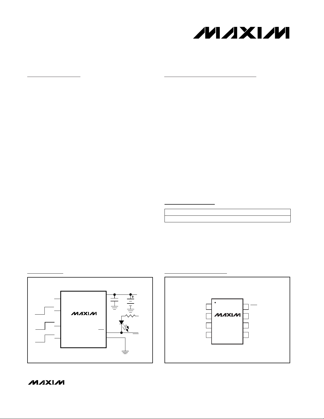
Pin Configuration
MAX1811
SELI
EN
SELV
IN
4.35V TO 6.5V
4.2V
4.1V
ON
OFF
100mA
500mA
BATT
GND
CHG
TO IN
TO LOAD
SINGLE
Li+
CELL
CHG
LOGIC OUT
LED
Typical Operating Circuit
19-2024; Rev 2; 6/03
Ordering Information
8 SO
PIN-PACKAGETEMP RANGE
-40°C to +85°CMAX1811ESA
PART
For pricing, delivery, and ordering information, please contact Maxim/Dallas Direct! at
1-888-629-4642, or visit Maxim’s website at www.maxim-ic.com.
* Protected by U.S. Patent # 6,507,172
TOP VIEW
SELV
1
2
GND
3
4
87CHG
MAX1811
SO
ENSELI
GND
6
BATTIN
5
Page 2
MAX1811
USB-Powered Li+ Charger
2 _______________________________________________________________________________________
ABSOLUTE MAXIMUM RATINGS
ELECTRICAL CHARACTERISTICS
(VIN= 4.5V, EN = IN, TA= 0°C to +85°C, unless otherwise noted.)
Stresses beyond those listed under “Absolute Maximum Ratings” may cause permanent damage to the device. These are stress ratings only, and functional
operation of the device at these or any other conditions beyond those indicated in the operational sections of the specifications is not implied. Exposure to
absolute maximum rating conditions for extended periods may affect device reliability.
IN, BATT, SELI, CHG, EN to GND ..............................-0.3V to 7V
SELV to GND ...............................................-0.3V to (V
IN
+ 0.3V)
Continuous Power Dissipation (TA= +70°C)
8-Pin SO (derate 17.5mW/°C above +70°C)....................1.4W
Short-Circuit Duration.................................................Continuous
Operating Temperature Range ...........................-40°C to +85°C
Storage Temperature Range .............................-65°C to +150°C
Maximum Die Temperature..............................................+150°C
Lead Temperature (soldering, 10s) .................................+300°C
Input Supply Voltage 4.35 6.50 V
Input Undervoltage Lockout IIN rising 3.75 4.05 V
Input Undervoltage Lockout Hysteresis 50 mV
Input Supply Current
Charging Headroom
Precondition Threshold
Precondition Threshold Hysteresis 80 mV
CHG Output Leakage Current VIN = V
CHG Output Low Voltage I
Charging Current
BATT Regulation Voltage
BATT Leakage Current (Input
Power Removed)
BATT Shutdown Current EN = GND, V
Logic Input Low Voltage (EN, SELI, SELV) VIN = 4.35V to 6.5V 0.8 V
Logic Input High Voltage (EN, SELI, SELV) V
Logic Input Leakage Current (EN, SELI) V
Logic Input Leakage Current (SELV) V
Thermal Regulation
PARAMETER CONDITIONS MIN TYP MAX UNITS
Operating, EN = IN, no load 0.9 2.0 mA
Shutdown, EN = GND 2.5 5.0 µA
SELI = GND (100mA mode),
= 4.35V
V
IN
SELI = IN (500mA mode) 200
BATT rising, transition from precondition to
charge mode
= 6.5V 0.1 1.0 µA
CHG
= 10mA 0.4 V
SINK
V
= V
SELI
= 5.5V, V
IN
SELI = GND, V
V
= 2V, SELI = GND or IN 20 43 70
BATT
SELV = GND, I
SELV = IN, I
V
BATT
= 4.35V to 6.5V 2.0 V
IN
= 0 to 6.5V; V
IN
= 0 to 6.5V, V
IN
BATT
= 4.2V, EN = IN = GND 1 5 µA
Die temperature beyond which charging
current is reduced
100
2.3 2.5 2.7 V
= 2.7V 455 500
BATT
= 5.5V, V
IN
= 0 4.08 4.10 4.12
BATT
= 2.7V 85 100
BATT
= 0 4.18 4.20 4.22
= 4.2V 0.1 2 µA
BATT
, VEN = 6.5V or GND 1 µA
SELI
= VIN or GND 1 µA
SELV
125 °C
mV
mA
V
Page 3
MAX1811
USB-Powered Li+ Charger
_______________________________________________________________________________________ 3
Typical Operating Characteristics
(CHG unconnected, C
BATT
= 2.2µF, TA = +25°C, unless otherwise noted.)
Note 1: Specifications to -40°C are guaranteed by design and not production tested.
ELECTRICAL CHARACTERISTICS
(VIN= 4.5V, TA= -40°C to +85°C, unless otherwise noted.) (Note1)
Input Supply Voltage 4.35 6.50 V
Input Undervoltage Lockout IIN rising 3.75 4.05 V
Input Supply Current
Precondition Threshold
BATT Regulation Voltage
BATT Leakage Current (Input
Power Removed)
BATT Shutdown Current EN = GND, V
PARAMETER CONDITIONS MIN TYP MAX UNITS
Operating, EN = IN, no load 3 mA
Shutdown, EN = GND 6 µA
BATT rising, transition from precondition to
charge mode
SELV = GND, I
SELV = IN, I
= 4.2V, IN = GND 10 µA
V
BATT
= 0 4.06 4.14
BATT
= 0 4.16 4.24
BATT
= 4.2V 3 µA
BATT
2.3 2.7 V
V
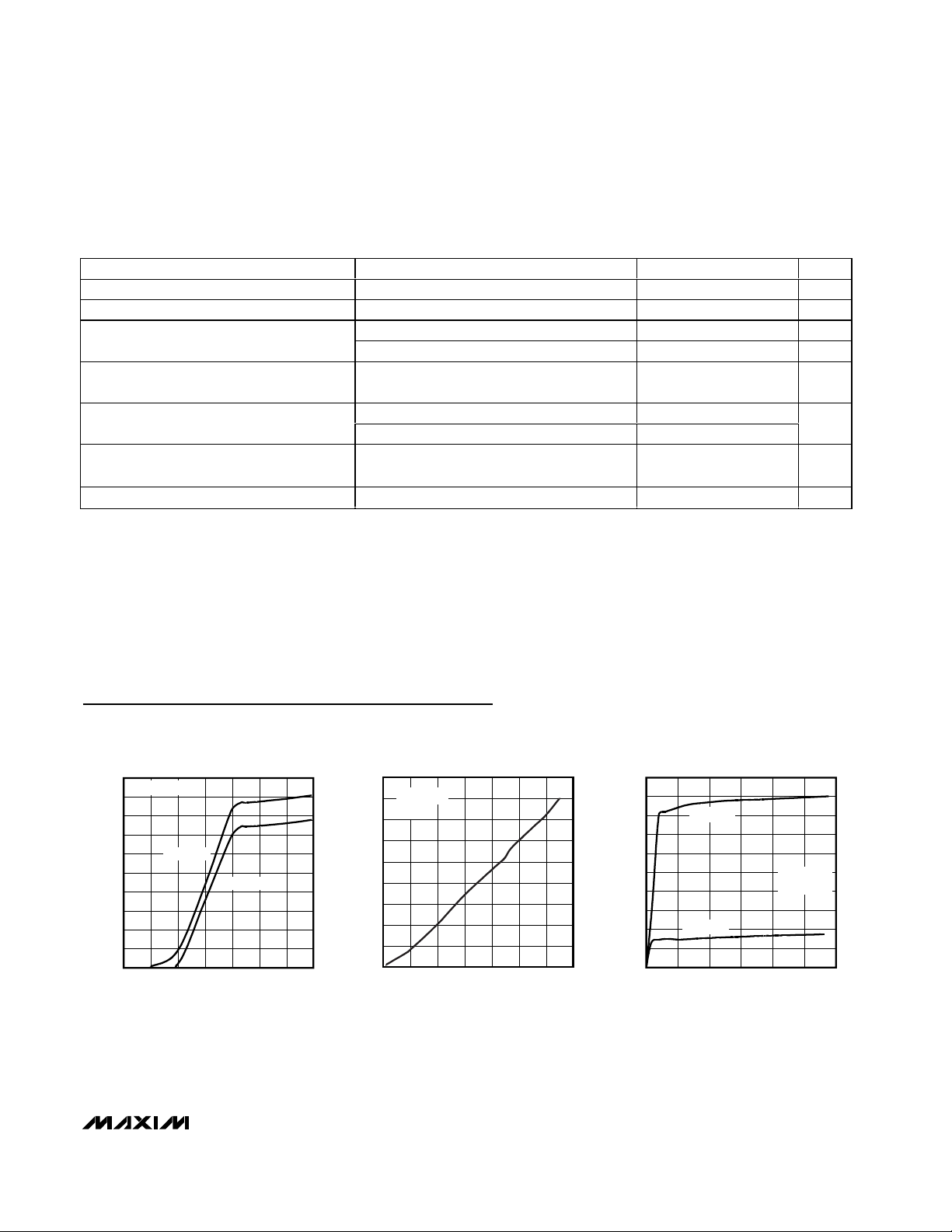
SUPPLY CURRENT
vs. INPUT VOLTAGE (ENABLED)
1.0
VIN = VEN = V
0.9
0.8
0.7
0.6
(mA)
0.5
IN
I
0.4
0.3
0.2
0.1
0
01234567
SELV
V
= V
SELI
IN
V
= 0
SELI
VIN (V)
MAX1811 toc01
SUPPLY CURRENT vs. INPUT VOLTAGE
4.5
4.0
VEN = 0
3.5
3.0
2.5
(µA)
IN
I
2.0
1.5
1.0
0.5
0
0231 4567
VIN = V
(SHUTDOWN)
SELV
VIN (V)
MAX1811 toc02
CHARGE CURRENT
vs. INPUT VOLTAGE HEADROOM
500
450
V
400
350
300
(mA)
250
BATT
I
200
150
100
50
0
0 1.00.5 1.5 2.0 2.5 3.0
= V
SELI
IN
V
= 0
SELI
VIN - V
(V)
BATT
MAX1811 toc03
V
= 4.1V
BATT
= V
V
SELV
IN
Page 4

MAX1811
USB-Powered Li+ Charger
4 _______________________________________________________________________________________
Typical Operating Characteristics (continued)
(CHG unconnected, C
BATT
= 2.2µF, TA = +25°C, unless otherwise noted.)
-50
50
0
200
150
100
250
300
450
400
350
500
0 1.0 1.50.5 2.0 2.5 3.0 3.5 4.0 4.5
CHARGE CURRENT
vs. BATTERY CURRENT
MAX1811 toc04
V
BATT
(V)
I
BATT
(mA)
VIN = VEN = V
SELV
= 5.5V
V
SELI
= V
IN
V
SELI
= 0
0
150
100
50
250
200
450
400
350
300
500
01234567
CHARGE CURENT
vs. INPUT VOLTAGE
MAX1811 toc05
VIN (V)
I
BATT
(mA)
V
BATT
= 4.1V
V
SELV
= V
IN
V
SELI
= V
IN
V
SELI
= 0
4.08
4.12
4.10
4.16
4.14
4.20
4.18
4.22
-40 10-15 35 60 85
BATTERY REGULATION VOLTAGE
vs. TEMPERATURE
MAX1811 toc06
TEMPERATURE (°C)
V
BATT
(V)
VIN = V
SELI
= VEN = 4.5V
I
BATT
= 0
V
SELV
= V
IN
V
SELV
= 0
0
200
100
400
300
500
600
-40 10-15 35 60 85
CHARGE CURRENT
vs. TEMPERATURE
MAX1811 toc07
TEMPERATURE (°C)
I
BATT
(mA)
VIN = V
SELV
= VEN = 5.5V, V
BATT
= 2.7V
V
SELI
= V
IN
V
SELI
= 0
0
200
100
400
300
500
600
-40 10-15 35 60 85
CHARGE CURRENT vs. TEMPERATURE
WITH THERMAL REGULATION
MAX1811 toc08
TEMPERATURE (°C)
I
BATT
(mA)
VIN = V
SELV
= VEN = 6.5V, V
BATT
= 2.7V
V
SELI
= V
IN
V
SELI
= 0
THERMAL CONTROL
LOOP IN OPERATION
Page 5

MAX1811
USB-Powered Li+ Charger
_______________________________________________________________________________________ 5
Pin Description
Figure 1. Functional Diagram
PIN NAME DESCRIPTION
1 SELV
Battery Regulation Voltage-Select Input. A low (< 0.8V) selects a 4.1V battery regulation set point. A high
(> 2.0V) selects a 4.2V battery regulation set point.
Battery Regulation Current-Select Input. A low (< 0.8V) selects a 100mA maximum battery regulation
2 SELI
current. A high (> 2.0V) selects a 500mA maximum battery regulation current. SELI is not diode clamped
to IN, and the voltage at V
can exceed the voltage at VIN.
SELI
3, 6 GND Ground. Connect pins 3 and 6 to a large copper trace for maximum power dissipation.
4 IN Input Supply Voltage. Bypass with a 4.7µF capacitor to GND.
5 BATT
7EN
8
CHG
Li+ Battery Connection. Bypass with a capacitor no less than 2.2µF to GND. High impedance in
shutdown.
Enable Input. A high (> 2.0V) enables the device. A low (< 0.8V) disables the device and places it into
shutdown mode. BATT is high impedance when disabled.
Charging Indicator Open-Drain Output. CHG pulls low while the device is in charge mode (2.5V
< V
< BATT Regulation Voltage).
BATT
VOLTAGE
LOOP
SELI
CURRENT
SELECTOR
IN
REGULATOR
3V
EN
BIAS
2V
MAX1811
THERMAL
LOOP
OVERCURRENT
DETECTOR
CURRENT
LOOP
MAX
DETECTOR
CIRCUIT
VOLTAGE
SELECTOR
SELV
CURRENT-
SENSE
CIRCUIT
(2.5V, 4.2V)
BATTERY
OVERVOLTAGE
DETECTOR
GND
BATT
CHG
4.7V
Page 6

MAX1811
USB-Powered Li+ Charger
6 _______________________________________________________________________________________
Figure 2. System Configuration
Detailed Description
Charger-Control Circuitry
The voltage/current regulator consists of a voltage control loop, a current control loop, and a thermal control
loop (Figure 1). Use the SELV input to set the battery
regulation voltage to a 4.1V or 4.2V single Li+ cell. The
current and thermal loops are internally compensated
and require no external compensation. The outputs
from all loops drive an internal linear regulator. The
thermal loop modulates the current loop by limiting the
charge current if the die temperature exceeds +125°C.
The MAX1811 is in current mode when the BATT voltage is below the regulation set point and in voltage
mode when the BATT voltage is near the regulation set
point. The CHG output indicates whether the part is in
current mode (CHG = low) or voltage mode (CHG =
high impedance). Battery voltages less than 2.5V activate a 43mA preconditioning mode (CHG = high
impedance). Normal charging resumes when the battery voltage exceeds 2.5V.
System Configuration
The MAX1811 is designed to operate seamlessly with a
universal serial bus (USB) port. In a typical design, the
USB connects to the MAX1811 input, and the MAX1811
drives the load and charges the battery when enabled.
Charge-Current Selection
The MAX1811 charges a single cell Li+ battery in either
100mA or 500mA modes. The MAX1811 expects the
system to poll the USB host to determine if the USB is
capable of providing 100mA or 500mA and regulates
the charging current accordingly (Figure 2). This is to
maintain compatibility with both powered and unpowered USB hosts. A powered USB host is capable of
providing 500mA, and an unpowered USB hub is limited to only 100mA.
Drive SELI low to set the charge current to the 100mA
mode. Use a 10kΩ pulldown resistor to ground on SELI,
if necessary, to ensure that the MAX1811 defaults to
the 100mA mode in the event that no logic signal is
present. Drive SELI high to increase the charge current
to the 500mA mode only if the polled USB port can provide the required current.
Thermal-Control Circuitry
The thermal loop limits the MAX1811 die temperature to
+125°C by reducing the charging current as necessary. The MAX1811 can operate normally with the thermal loop active. This is not a fault condition and can be
used continuously. The power dissipated by the internal power FET is determined by (VIN- V
BATT
) ✕I
CHG
.
The power dissipation rating for the thermally enhanced
8-pin SO package is 1.4W at +50°C ambient (assuming
a 1in2PC board radiating area), which is the maximum
ambient temperature at which most Li+ battery manufacturers allow charging. The 1.4W power dissipation
may never be reached due to the MAX1811’s thermal
regulation loop.
Applications Information
USB Output Voltage
The minimum voltage to a USB-powered device may
be as low as 4.35V when cable and connector drops
are considered (Figure 3). The MAX1811 is optimized
for operation at these low input voltage levels. USB
hubs may also provide as much as 5.5V. At high input
voltages (5.5V) and low cell voltages (2.7V), the
MAX1811’s thermal loop may limit the charge current
until the cell voltage rises.
USB*
PORT
4.35V TO 5.5V
*WHEN USING WALL ADAPTER, IN VOLTAGE RANGE IS FROM 4.35V TO 6.5V.
IN
MAX1811
BATT
SINGLE
Li+
CELL
SYSTEM
LOAD
Page 7

MAX1811
USB-Powered Li+ Charger
_______________________________________________________________________________________ 7
Charging from AC Adapters
The MAX1811 also operates from sources other than
USB ports. The full charging input voltage range is
4.35V to 6.5V. When charging in the 500mA mode with
an AC adapter, rely on the thermal loop to limit the
power dissipation by limiting the charge current at
higher input voltages if limited PC board area is available to dissipate heat.
Capacitor Selection
Use a minimum of 2.2µF placed close to BATT for proper stability. Bypass IN to GND with a 4.7µF capacitor.
Use a larger input bypass capacitor for high input voltages or high charging current to reduce supply noise.
Chip Information
TRANSISTOR COUNT: 1907
PROCESS: BiCMOS
Figure 3. USB Voltage Specification
Figure 4. Charging from a USB Port
HOST OR
POWERED HUB
4.750V
0.000V
*UNDER TRANSIENT CONDITIONS, SUPPLY AT HUB CAN DROP FROM 4.00V TO 4.070V.
4.735V
0.015V
4.640V
0.110V
BUS-POWERED
4.625V
4.500V
0.125V
REFERENCED
TO SOURCE
LOW-POWER
HUB
*4.400V
0.000V
REFERENCED
TO HUB
4.397V
0.003V
4.378V
0.002V
FUNCTION
4.375V
4.350V
0.025V
4.35V TO 6.5V
4.2V
4.1V
ON
OFF
500mA
100mA
10k
IN
SELV
MAX1811
EN
SELI
Ω
BATT
CHG
GND
GND
LED
TO LOAD
SINGLE
Li+
CELL
TO IN
CHG
LOGIC OUT
Page 8

MAX1811
USB-Powered Li+ Charger
Maxim cannot assume responsibility for use of any circuitry other than circuitry entirely embodied in a Maxim product. No circuit patent licenses are
implied. Maxim reserves the right to change the circuitry and specifications without notice at any time.
8 _____________________Maxim Integrated Products, 120 San Gabriel Drive, Sunnyvale, CA 94086 408-737-7600
© 2003 Maxim Integrated Products Printed USA is a registered trademark of Maxim Integrated Products.
Package Information
(The package drawing(s) in this data sheet may not reflect the most current specifications. For the latest package outline information,
go to www.maxim-ic.com/packages.)
N
1
e
FRONT VIEW
TOP VIEW
D
INCHES
DIM
MIN
0.053A
0.004
A1
0.014
B
0.007
C
e 0.050 BSC 1.27 BSC
0.150
H
E
A
B
A1
C
L
E
H 0.2440.228 5.80 6.20
0.016L
VARIATIONS:
INCHES
MINDIM
D
0.189 0.197 AA5.004.80 8
D
0.337 0.344 AB8.758.55 14
0.386D
0-8
MAX
0.069
0.010
0.019
0.010
0.157
0.050
MAX
0.394
MILLIMETERS
MAX
MIN
1.35
1.75
0.10
0.25
0.35
0.49
0.19
0.25
3.80 4.00
0.40 1.27
MILLIMETERS
MAX
MIN
9.80 10.00
N MS012
16
AC
SOICN .EPS
SIDE VIEW
PROPRIETARY INFORMATION
TITLE:
PACKAGE OUTLINE, .150" SOIC
APPROVAL
21-0041
REV.DOCUMENT CONTROL NO.
1
B
1
 Loading...