

Page 1
General Description
The MAX1762/MAX1791 PWM step-down controllers
provide high efficiency, excellent transient response,
and high DC output accuracy needed for stepping
down high-voltage batteries to generate low-voltage
CPU core, I/O, and chipset RAM supplies in notebook
computers and PDAs.
Maxim’s proprietary Quick-PWM™ pulse-width modulator is a free-running constant on-time type with input
feed-forward. Its high operating frequency (300kHz)
allows small external components to be utilized in PC
board area-critical applications such as subnotebook
computers and smart phones. PWM operation occurs
at heavy loads, and automatic switchover to pulse-skipping operation occurs at lighter loads. The external
high-side p-channel and low-side n-channel MOSFETs
require no bootstrap components. The MAX1762/
MAX1791 are simple, easy to compensate, and do not
have the noise sensitivity of conventional fixed-frequency current-mode PWMs.
These devices achieve high efficiency at a reduced
cost by eliminating the current-sense resistor found in
traditional current-mode PWMs. Efficiency is further
enhanced by their ability to drive synchronous-rectifier
MOSFETs. The MAX1762/MAX1791 come in a 10-pin
µMAX package and offer two fixed voltages (Dual
Mode™) for each device, 1.8V/2.5V/adj (MAX1762) and
3.3V/5.0V/adj (MAX1791).
________________________Applications
Notebooks Handy-Terminals
Subnotebooks PDAs
Digital Cameras Smart Phones
1.8V/2.5V Logic
and I/O Supplies
Features
♦ High Operating Frequency (300kHz)
♦ No Current-Sense Resistor
♦ Accurate Current Limit
♦ ±1% Total DC Error over Line and During
Continuous Conduction
♦ Dual Mode Fixed Output
1.8V/2.5V/adj (MAX1762)
3.3V/5.0V/adj (MAX1791)
♦ 0.5V to 5.5V Output Adjust Range
♦ 5V to 20V Input Range
♦ Automatic Light-Load Pulse Skipping Operation
♦ Free-Running On-Demand PWM
♦ Foldback Mode™ UVLO
♦ PFET/NFET Synchronous Buck
♦ 4.65V at 25mA Linear Regulator Output
♦ 5µA Shutdown Supply Current
♦ 230µA Quiescent Supply Current
♦ 10-Pin µMAX Package
MAX1762/MAX1791
High-Efficiency, 10-Pin µMAX, Step-Down
Controllers for Notebooks
________________________________________________________________ Maxim Integrated Products 1
19-1923; Rev 1; 10/05
EVALUATION KIT
AVAILABLE
Ordering Information
PART TEMP RANGE
PIN-PACKAGE
MAX1762EUB -40°C to +85°C 10 µMAX
MAX1791EUB -40°C to +85°C 10 µMAX
FB
GND
CS
DH
VP
DL
OUT
REF
SHDN
V
BATT
(5V TO 20V)
V
OUT
1.8V/3.3V
VL
MAX1762
MAX1791
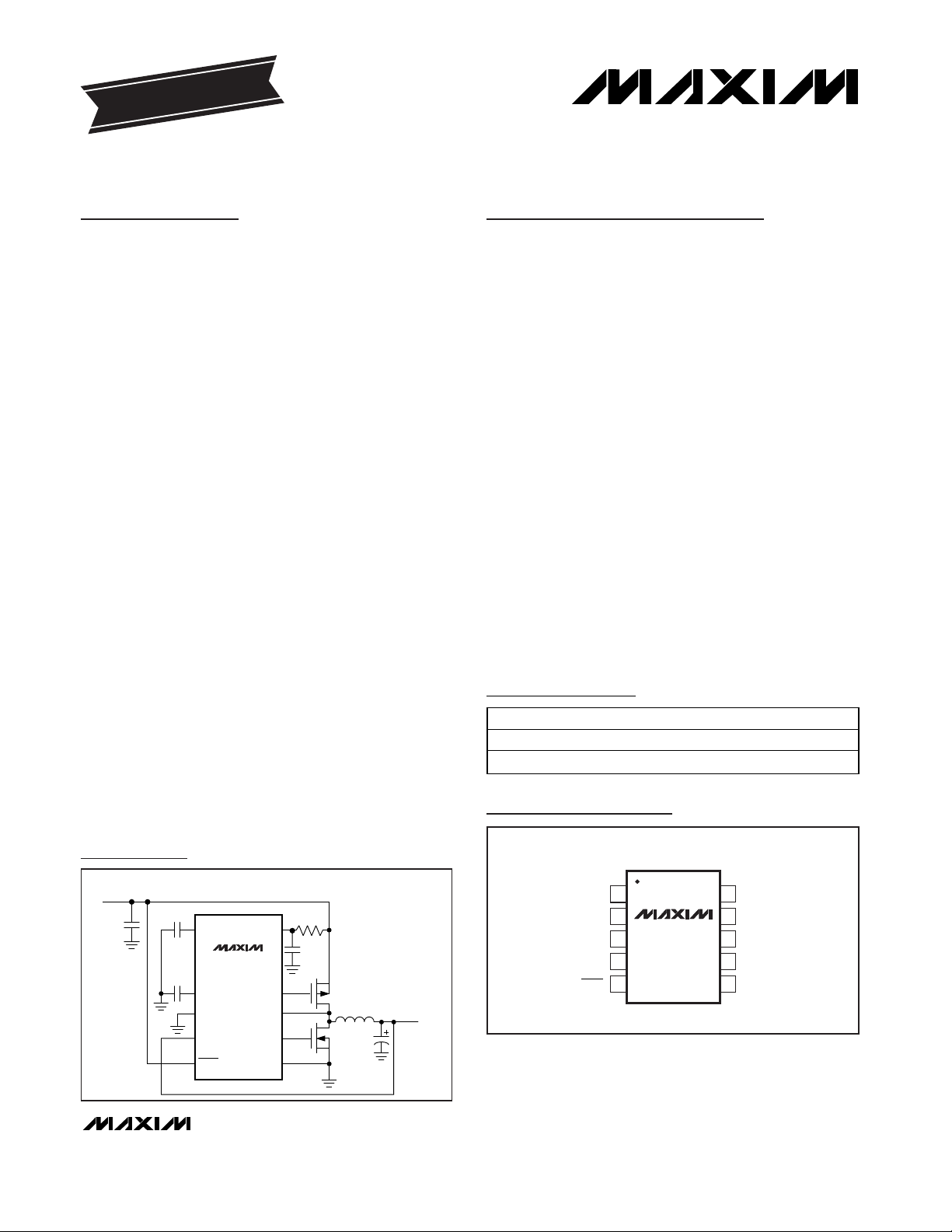
Typical Operating Circuit
1
2
3
4
5
10
9
8
7
6
DH
CS
DLOUT
FB
REF
VL
MAX1762
MAX1791
µMAX
TOP VIEW
GNDSHDN
VP
Pin Configuration
For price, delivery, and to place orders, please contact Maxim Distribution at 1-888-629-4642,
or visit Maxim’s website at www.maxim-ic.com.
Quick-PWM, Dual Mode, and Foldback Mode are a trademarks of Maxim Integrated Products, Inc.
Page 2
MAX1762/MAX1791
High-Efficiency, 10-Pin µMAX, Step-Down
Controllers for Notebooks
2 _______________________________________________________________________________________
ABSOLUTE MAXIMUM RATINGS
VP, SHDN to GND ..................................................-0.3V to +22V
VP to VL ..................................................................-0.3V to +22V
OUT, VL to GND .......................................................-0.3V to +6V
DL, FB, REF to GND ....................................-0.3V to (VL + 0.3V)
DH to GND....................................................-0.3V to (VP + 0.3V)
CS to GND ....................................................-2.0V to (VP + 0.3V)
REF Short Circuit to GND ...........................................Continuous
Continuous Power Dissipation (T
A
= +70°C)
10-Pin µMAX (derate 5.6mW/°C above +70°C) ...........444mW
Operating Temperature Range ...........................-40°C to +85°C
Junction Temperature......................................................+150°C
Storage Temperature Range .............................-65°C to +150°C
Lead Temperature (soldering, 10s) .................................+300°C
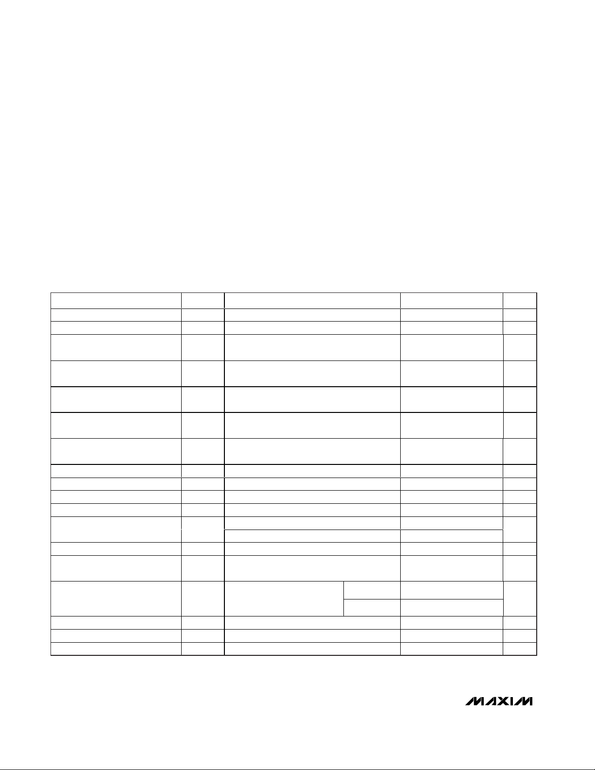
ELECTRICAL CHARACTERISTICS
(VVP= 15V, VL enabled, CVL= 1µF, C
REF
= 0.1µF,
T
A
= 0 to +85°C,
unless otherwise noted. Typical values are at T
A
= +25°C.)
(Note 1)
PARAMETER
CONDITIONS
UNITS
VP Input Voltage Range V
VP
520V
VL Input Voltage Range V
VL
VL (overdriven)
V
OUT Output Voltage
(MAX1762, 1.8V Fixed)
V
OUT
VVP = 5V to 20V, VVL = 4.75V to 5.25V,
FB = GND, continuous conduction mode
1.8
V
OUT Output Voltage
(MAX1762, 2.5V Fixed)
V
OUT
VVP = 5V to 20V, VVL = 4.75V to 5.25V,
FB = VL, continuous conduction mode
2.5
V
OUT Output Voltage
(MAX1791, 3.3V Fixed)
V
OUT
VVP = 5V to 20V, VVL = 4.75V to 5.25V,
FB = GND, continuous conduction mode
3.3
V
OUT Output Voltage
(MAX1791, 5V Fixed)
V
OUT
VVP = 7V to 20V, VVL = 4.75V to 5.25V,
FB = VL, continuous conduction mode
5
V
OUT Output Voltage (Adj Mode)
VVP = 5V to 20V, VVL = 4.75V to 5.25V,
FB = OUT, continuous conduction mode
V
Output Voltage Adjust Range 0.5 5.5 V
OUT Input Resistance Adjustable-output mode
kΩ
FB Input Bias Current VFB = 1.3V
0.1 µA
Soft-Start Ramp Time Zero to full I
LIM
µs
V
OUT
= 1.25V, VVP = 6V
On-Time (Note 2) t
ON
V
OUT
= 5V, VVP = 6V
ns
Minimum Off-Time t
OFF
(Note 2)
ns
VL Quiescent Supply Current
FB = GND, V
VL
= 5V, OUT forced above the
regulation point
µA
VVL = float
VP Quiescent Supply Current
FB = GND, OUT forced
above the regulation point,
V
VP
= 20V
V
VL
= 5V 93
µA
VL Shutdown Supply Current VVL = 5V, SHDN = GND 2 15 µA
VP Shutdown Supply Current
412µA
VL Output Voltage I
LOAD
= 0 to 25mA, VVP = 5V to 20V 4.5
V
Stresses beyond those listed under “Absolute Maximum Ratings” may cause permanent damage to the device. These are stress ratings only, and functional
operation of the device at these or any other conditions beyond those indicated in the operational sections of the specifications is not implied. Exposure to
absolute maximum rating conditions for extended periods may affect device reliability.
SYMBOL
MIN TYP MAX
S HD N = GN D , m easur ed at V P , V
= 0 or 5V
V L
4.75 5.25
1.773
2.463
3.250
4.925
1.231 1.250 1.269
300 800 1700
-0.1
666 740 814
2550 2830 3110
300 400 500
1700
153 260
227 410
4.65 4.75
1.827
2.538
3.350
5.075
200
Page 3
MAX1762/MAX1791
High-Efficiency, 10-Pin µMAX, Step-Down
Controllers for Notebooks
_______________________________________________________________________________________ 3
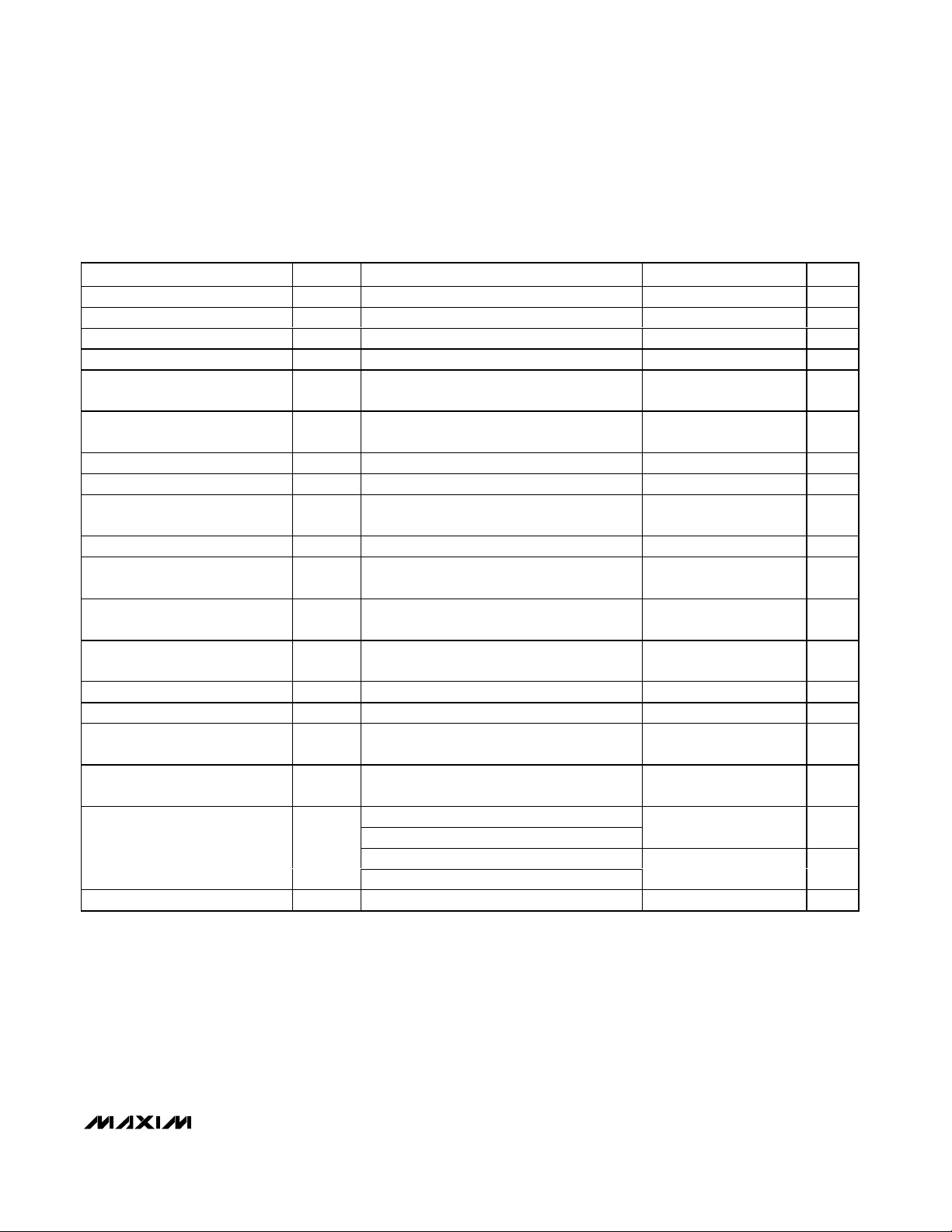
ELECTRICAL CHARACTERISTICS (continued)
(VVP= 15V, VL enabled, CVL= 1µF, C
REF
= 0.1µF,
T
A
= 0 to +85°C,
unless otherwise noted. Typical values are at T
A
= +25°C.)
(Note 1)
PARAMETER
CONDITIONS
UNITS
Reference Voltage VVL = 4.75V to 5.25V, no load
2
V
Reference Load Regulation I
REF
= 0 to 50µA
V
REF Sink Current REF in regulation 10 µA
REF Fault Lockout Voltage Falling edge 1.6 V
Output Undervoltage Threshold
(Foldback)
With respect to regulation point, no load 60 70 80 %
Output Undervoltage Lockout
Time (Foldback)
From SHDN signal going high V
OUT
< 0.6 x
regulation point
10 20 42 ms
Current-Limit Threshold V
ILIM
-90
mV
Thermal Shutdown Threshold Hysteresis = 10oC
o
C
VL Undervoltage Lockout
Threshold
Rising edge, hysteresis = 20mV, PWM
disabled below this level
4.1 4.4 V
DH Gate Driver On-Resistance VVP = 6V to 20V, measure at 50mA 5 8 Ω
DL Gate Driver On-Resistance
(Pullup)
DL, high state, measure at 50mA 5 8 Ω
DL Gate Driver On-Resistance
(Pulldown)
DL, low state, measure at 50mA 1 5 Ω
DH Gate Driver Source/Sink
Current
V
DH
= 3V, VVP = 6V 0.6 A
DL Gate Driver Sink Current VDL = 2.5V 0.9 A
DL Gate Driver Source Current V
DL
= 2.5V 0.5 A
SHDN Logic Input High
Threshold Voltage
V
IH
1.6 V
SHDN Logic Input Low
Threshold Voltage
V
IL
0.6 V
MAX1762 V
OUT
= 1.8V fixed
MAX1791 V
OUT
= 3.3V fixed
50
mV
MAX1762 V
OUT
= 2.5V fixed
Dual Mode Threshold Voltage
MAX1791 V
OUT
= 5V fixed
2.5
4V
SHDN Logic Input Current SHDN = 0 or 5V -2 +2 µA
SYMBOL
MIN TYP MAX
1.98
-100 -110
160
100 150
3.25
2.02
0.01
Page 4
MAX1762/MAX1791
High-Efficiency, 10-Pin µMAX, Step-Down
Controllers for Notebooks
4 _______________________________________________________________________________________
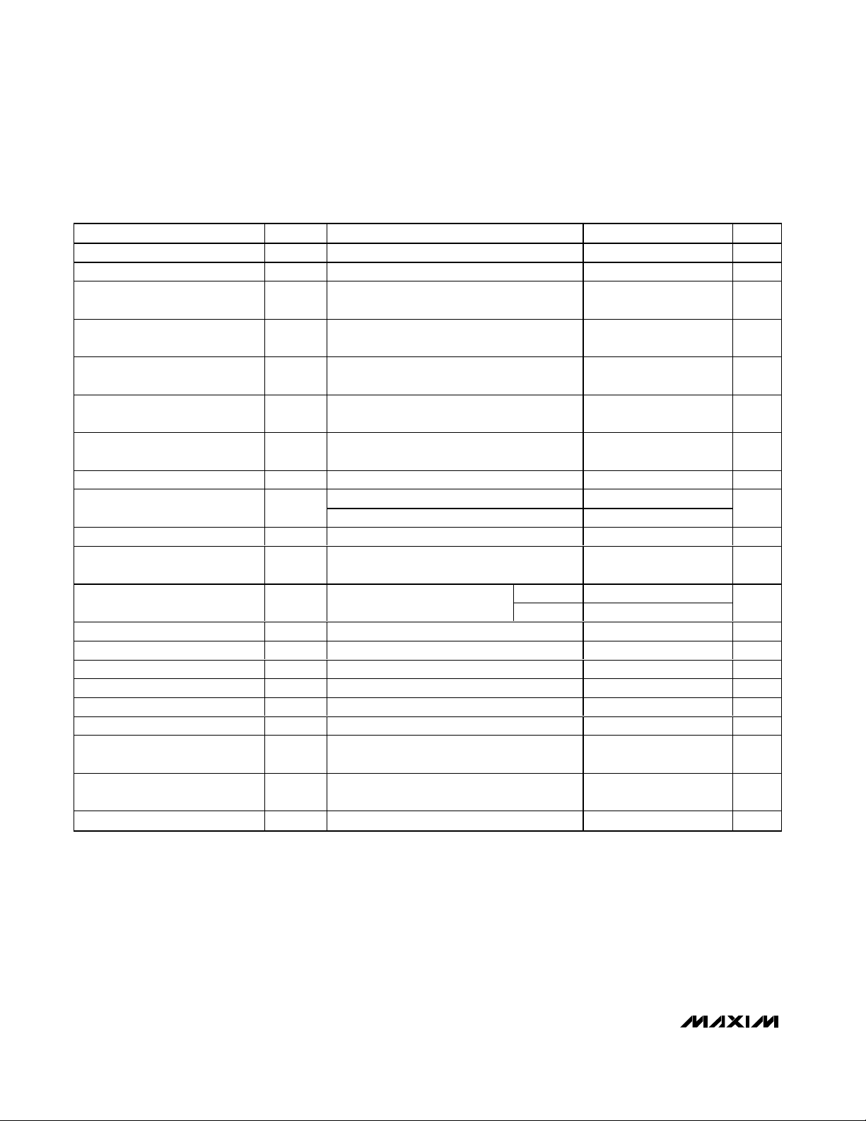
ELECTRICAL CHARACTERISTICS
(VVP= 15V, VL enabled, CVL= 1µF, C
REF
= 0.1µF,
T
A
= -40 to +85°C,
unless otherwise noted.) (Note 1)
PARAMETER
SYMBOL
CONDITIONS
MIN
TYP
MAX
UNITS
VP Input Voltage Range V
VP
520V
VL Input Voltage Range V
VL
VL (overdriven)
V
OUT Output Voltage
(MAX1762, 1.8V Fixed)
V
OUT
VVP = 5V to 20V, VVL = 4.75V to 5.25V,
FB = GND, continuous conduction mode
V
OUT Output Voltage
(MAX1762, 2.5V Fixed)
V
OUT
VVP = 5V to 20V, VVL = 4.75V to 5.25V,
FB = VL, continuous conduction mode
V
OUT Output Voltage
(MAX1791, 3.3V Fixed)
V
OUT
VVP = 5V to 20V, VVL = 4.75V to 5.25V,
FB = GND, continuous conduction mode
V
OUT Output Voltage
(MAX1791, 5V Fixed)
V
OUT
VVP = 7V to 20V, VVL = 4.75V to 5.25V,
FB = VL, continuous conduction mode
V
OUT Output Voltage (adj Mode)
VVP = 5V to 20V, VVL = 4.75V to 5.25V,
FB = OUT, continuous conduction mode
V
FB Input Bias Current VFB = 1.3V
0.2 µA
V
OUT
= 1.25V, VVP = 6V
On-Time (Note 2) t
ON
V
OUT
= 5V, VVP = 6V
ns
Minimum Off-Time t
OFF
(Note 2)
ns
VL Quiescent Supply Current
FB = GND, V
VL
= 5V, OUT forced above the
regulation point
µA
VP Quiescent Supply Current
FB = GND, OUT forced above
the regulation point V
VP
= 20V
µA
VL Shutdown Supply Current VVL = 5V, SHDN = GND 15 µA
VP Shutdown Supply Current
12 µA
VL Output Voltage I
LOAD
= 0 to 25mA, VVP = 5V to 20V 4.5
V
Reference Voltage VVL = 4.75V to 5.25V, no load
V
Reference Load Regulation I
REF
= 0 to 50µA
V
REF Sink Current REF in regulation 10 µA
Output Undervoltage Threshold
(Foldback)
With respect to regulation point, no load 60 80 %
Output Undervoltage Lockout
Time (Foldback)
From SHDN signal going high, V
OUT
< 0.6 x
regulation point
10 42 ms
Current-Limit Threshold V
ILIM
-90
mV
4.75 5.25
1.773 1.827
2.463 2.538
3.250 3.350
4.925 5.075
1.231 1.269
S HD N = GN D , m easur ed at V P , V
V
= float 410
V L
V
= 5V 200
V L
= 0 or 5V
V L
-0.2
666 814
2550 3110
250 550
1.98 2.02
260
4.75
0.01
-110
Page 5
MAX1762/MAX1791
High-Efficiency, 10-Pin µMAX, Step-Down
Controllers for Notebooks
_______________________________________________________________________________________ 5
Note 1:
Specifications to -40°C are guaranteed by design, not production tested.
Note 2:
One-shot times are measured at the DH pin (VP = 15V, C
DH
= 400pF, 90% point to 90% point; see drawing below for
measurement details).
ELECTRICAL CHARACTERISTICS (continued)
(VVP= 15V, VL enabled, CVL= 1µF, C
REF
= 0.1µF,
T
A
= -40 to +85°C,
unless otherwise noted.) (Note 1)
PARAMETER
CONDITIONS
UNITS
VL Undervoltage Lockout
Threshold
Rising edge, hysteresis = 20mV, PWM
disabled below this level
4.1 4.4 V
SHDN Logic Input High
Threshold Voltage
V
IH
1.6 V
SHDN Logic Input Low
Threshold Voltage
V
IL
0.6 V
MAX1762 V
OUT
= 1.8V fixed
MAX1791 V
OUT
= 3.3V fixed
50
mV
MAX1762 V
OUT
= 2.5V fixed
Dual Mode Threshold Voltage
MAX1791 V
OUT
= 5V fixed
2.5 4 V
DH
90% 90%
SYMBOL
t
ON
MIN TYP MAX
150
Page 6
MAX1762/MAX1791
High-Efficiency, 10-Pin µMAX, Step-Down
Controllers for Notebooks
6 _______________________________________________________________________________________
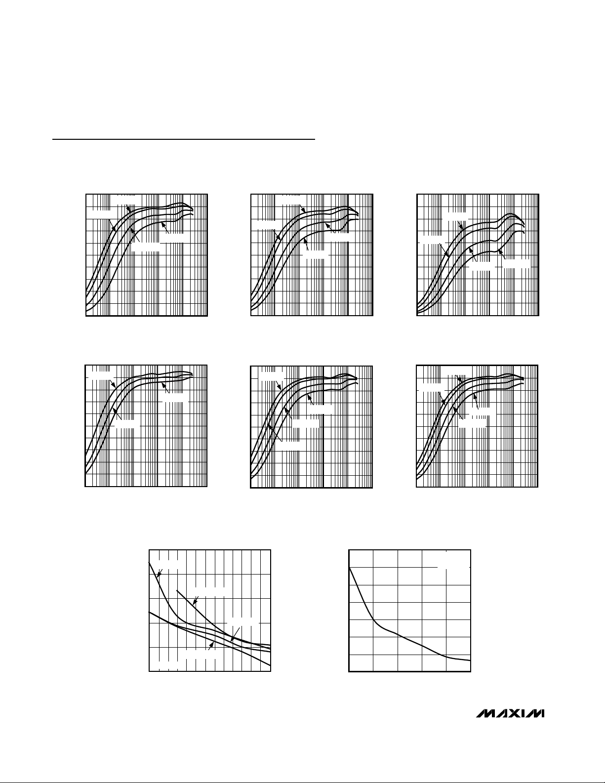
Typical Operating Characteristics
(TA = +25°C, unless otherwise noted.)
100
0
0.1 1 10 100 1000 10,000
MAX1762
EFFICIENCY vs. LOAD (2.5V)
20
MAX1762/91 toc01
LOAD CURRENT (mA)
EFFICIENCY (%)
40
60
80
10
30
50
70
90
VVP = 5V
VVP = 12V
VVP = 7V
VVP = 18V
100
0
0.1 1 10 100 1000 10,000
MAX1791
EFFICIENCY vs. LOAD (3.3V)
20
MAX1762/91 toc05
LOAD CURRENT (mA)
EFFICIENCY (%)
40
60
80
10
30
50
70
90
VVP = 18V
VVP = 12V
VVP = 7V
VVP = 5V
100
0
0.1 1 10 100 1000 10,000
MAX1791
EFFICIENCY vs. LOAD (3.0V)
20
MAX1762/91 toc06
LOAD CURRENT (mA)
EFFICIENCY (%)
40
60
80
10
30
50
70
90
VVP = 7V
VVP = 18V
VVP = 12V
VVP = 5V
-0.6
-0.4
-0.5
-0.2
-0.3
0
-0.1
0.1
0105152025
VL VOLTAGE ERROR vs. OUTPUT CURRENT
MAX1762/91 toc08
VL CURRENT (mA)
VL VOLTAGE ERROR (%)
VVP = 12V
V
OUT
= 2.5V
100
0
0.1 1 10 100 1000 10,000
MAX1791
EFFICIENCY vs. LOAD (5V)
20
MAX1762/91 toc04
LOAD CURRENT (mA)
EFFICIENCY (%)
40
60
80
10
30
50
70
90
VVP = 7V
VVP = 18V
VVP = 12V
250
275
325
300
350
375
FREQUENCY vs. SUPPLY VOLTAGE
MAX1762/91 toc07
SUPPLY VOLTAGE (V)
FREQUENCY (kHz)
51181417
V
OUT
= 3.3V
V
OUT
= 5.0V
V
OUT
= 2.5V
V
OUT
= 1.8V
LOAD = 1A
100
0
0.1 1 10 100 1000 10,000
MAX1762
EFFICIENCY vs. LOAD (1.8V)
20
MAX1762/91 toc02
LOAD CURRENT (mA)
EFFICIENCY (%)
40
60
80
10
30
50
70
90
VVP = 18V
VVP = 12V
VVP = 5V
VVP = 7V
100
0
0.1 1 10 100 1000 10,000
MAX1762
EFFICIENCY vs. LOAD (1V)
20
MAX1762/91 toc03
LOAD CURRENT (mA)
EFFICIENCY (%)
40
60
80
10
30
50
70
90
VVP = 7V
VVP = 12V
VVP = 5V
VVP = 18V
Page 7

MAX1762/MAX1791
High-Efficiency, 10-Pin µMAX, Step-Down
Controllers for Notebooks
_______________________________________________________________________________________ 7
Typical Operating Characteristics (continued)
(TA = +25°C, unless otherwise noted.)
LOAD-TRANSIENT RESPONSE
MAX1762/91 toc12
V
OUT
AC-COUPLED
100mV/div
I
L
2A/div
100µs/div
V
VP
= 12V, IL = 0 TO 2A, V
OUT
= 2.5V
LOAD-TRANSIENT RESPONSE
MAX1762/91 toc13
V
OUT
AC-COUPLED
100mV/div
I
LOAD
2A/div
100µs/div
V
VP
= 12V, I
LOAD
= 0 TO 2A, V
OUT
= 1.8V
LINE-TRANSIENT RESPONSE
MAX1762/91 toc11
VP
1V/div
7V
V
OUT
AC-COUPLED
20mV/div
100µs/div
V
VP
= 7.5V TO 8V, I
LOAD
= 0, V
OUT
= 2.5V
SHUTDOWN AND STARTUP WAVEFORMS
(I
L
= 300mA)
MAX1762/91 toc15
V
OUT
2V/div
I
LX
1A/div
SHDN
5V/div
2ms/div
V
VP
= 8V, I
LOAD
= 300mA, V
OUT
= 2.5V
SHUTDOWN AND STARTUP WAVEFORMS
(I
L
= 2.5A)
MAX1762/91 toc16
I
LX
2A/div
SHDN
5V/div
V
OUT
2V/div
2ms/div
V
VP
= 8V, I
LOAD
= 2.5A, V
OUT
= 2.5V
OUTPUT OVERLOAD WAVEFORMS
MAX1762/91 toc14
100µs/div
V
VP
= 12V, I
LOAD
= 0 TO 3A, V
OUT
= 2.5V
V
OUT
AC-COUPLED
I
LOAD
2A/div
4.0
4.6
4.4
4.2
4.8
5.0
5.2
5.4
5.6
5.8
6.0
51181417
SUPPLY CURRENT vs. INPUT VOLTAGE
(SHUTDOWN)
MAX1762/91 toc10
VP (V)
SUPPLY CURRENT (µA)
NO LOAD
0
100
50
200
150
250
300
51181417
SUPPLY CURRENT vs. INPUT VOLTAGE
MAX1762/91 toc09
VP (V)
SUPPLY CURRENT (µA)
V
OUT
= 3.3V
NO LOAD
Page 8

MAX1762/MAX1791
High-Efficiency, 10-Pin µMAX, Step-Down
Controllers for Notebooks
8 _______________________________________________________________________________________
Standard Application Circuit
The standard application circuit (Figure 1) generates a
low-voltage output for general-purpose use in notebook
computers (I/O supply, fixed CPU, core supply, and
DRAM supply). This DC-DC converter steps down battery voltage from 5V to 20V with high efficiency and
accuracy to a fixed voltage of 1.8V/2.5V/adj (MAX1762)
or 3.3V/5.0V/adj (MAX1791). Both the MAX1762 and
MAX1791 can be configured for adjustable output voltages (V
OUT
> 1.25V), using a resistive voltage-divider
from V
OUT
to FB to adjust the output voltage (Figure 2).
Similarly, Figure 3 shows an application circuit for V
OUT
< 1.25V, where a resistive voltage-divider from REF to
FB is used to set the output voltage. Figure 4 shows
how to set the regulator’s current limit with an external
sense resistor from CS to GND. Table 1 lists the components for each application circuit, and Table 2 contains contact information for the component
manufacturers.
Detailed Description
The MAX1762/MAX1791 step-down controllers are targeted at low-voltage chipsets and RAM power supplies
for notebook and subnotebook computers, with additional applications in digital cameras, PDAs, and
handy-terminals. Maxim’s proprietary Quick-PWM
pulse-width modulator (Figure 5) is specifically
designed for handling fast load steps while maintaining
a relatively constant operating frequency (300kHz) over
a wide range of input voltages (5V to 20V). The
MAX1762 has fixed 1.8V or 2.5V outputs, while the
MAX1791 has fixed 3.3V or 5.0V output voltages. Using
an external resistive divider, V
OUT
can be set between
0.5V and 5.5V on either device. Quick-PWM architecture circumvents the poor load-transient response of
fixed-frequency current-mode PWMs. This type of
design avoids the problems commonly encountered
with conventional constant-on-time and constant-offtime PWM schemes.
PIN NAME FUNCTION
1VL
+4.65V Linear Regulator Output. Serves as the supply input for the DL gate driver and supplies up to
25mA to external loads. VL can be overdriven using an external 5V supply. Bypass VL to GND with
at least a 1µF ceramic capacitor.
2 REF
2V Reference Voltage Output. Bypass to GND with 0.1µF ceramic capacitor. REF can deliver up to
50µA for external loads.
3FB
Feedback Input. Connect to an external resistive divider from OUT to GND in adjustable version.
Regulates to 1.25V. FB also serves as Dual Mode select pin. Connect FB to GND for a fixed 1.8V
( M AX 1762) or 3.3V (M AX 1791) outp ut, or to VL for a fi xed 2.5V (M AX 1762) or 5.0V ( M AX 1791) outp ut.
4 OUT
Output Voltage Connection. OUT is used for sensing the output voltage to determine the on-time and
also serves as the feedback input in fixed-output modes.
5 SHDN
Shutdown Input. Connect to a voltage less than V
IL
(<0.6V) to shut down the device. Connect to a
voltage greater than V
IH
(>1.6V) for normal operation.
6 GND Analog and Power Ground
7DLLow-Side Gate Driver Output. DL swings between VL and GND.
8CS
Current-Sense Connection. For lossless current sensing, connect CS to the junction of the MOSFETs
and inductor. For more accurate current sensing, connect CS to a current-sense resistor from the
source of the low-side switch to GND.
9DHHigh-Side Gate Driver Output. DH swings between VP and GND.
10 VP
Battery Voltage Supply Input. Used for PWM one-shot timing and as the input for the VL regulator
and DH gate drivers.
Pin Description
Page 9

MAX1762/MAX1791
High-Efficiency, 10-Pin µMAX, Step-Down
Controllers for Notebooks
_______________________________________________________________________________________ 9
Figure 1. Typical Application Circuit for Fixed Voltage
FB
Q1
L1
7µH
Q2
C2
1µF
C3
0.1µF
GND
C1
10µF
CS
DH
C4
220µF
VP
DL
OUT
REF
SHDN
V
VP
V
OUT
VL
MAX1762
MAX1791
10Ω
1µF
Figure 2. Typical Application Circuit for Adjustable Output V
OUT
> 1.25V
FB
Q1
R1
R2
L1
7µH
Q2
C2
1µF
C3
0.1µF
GND
C1
10µF
CS
DH
C4
220µF
VP
DL
OUT
REF
SHDN
V
VP
V
OUT
VL
MAX1762
MAX1791
10Ω
1µF
Figure 3. Typical Application Circuit for V
OUT
< 1.25V
FB
Q1
R1
R2
L1
7µH
Q2
C2
1µF
C3
0.1µF
GND
C1
10µF
CS
DH
C4
220µF
VP
DL
OUT
REF
SHDN
V
VP
V
OUT
VL
MAX1762
MAX1791
10Ω
1µF
Page 10

MAX1762/MAX1791
High-Efficiency, 10-Pin µMAX, Step-Down
Controllers for Notebooks
10 ______________________________________________________________________________________
Figure 4. Operation with External Current-Sense Resistor
FB
Q1
R
S
L1
10µH
Q2
C2
1µF
C3
0.1µF
GND
C1
10µF
CS
DH
C4
150µF
VP
DL
OUT
REF
SHDN
V
VP
V
OUT
VL
MAX1762
MAX1791
10Ω
1µF
Table 1. Component Selection for Standard Applications
COMPONENT 1.8V/2.5V/3.3V/5.0V AT 2A 1V AT 2A
Input Voltage Range 5V to 20V 5V to 20V
Inductor (µH) 7 5.2
L1 Inductor
CDRH104-7R0NC
Sumida
CDRH104-5R2NC
Sumida
Q1 MOSFETS
NDS8958A
Fairchild
SI4539ADY
Fairchild
C1 Input Capacitor
TMK432BJ106KM
Taiyo Yuden
TMK432BJ106
Taiyo Yuden
C2 VL Cap
EMK3160J105KL
Taiyo Yuden
LMK316BJ475
Taiyo Yuden
C3 REF Cap
UMK316BI104KH
Taiyo Yuden
UMK316BI104KH
Taiyo Yuden
C4 Output Cap
10TPB220M
Sanyo
6TPB150M
Sanyo
Page 11

MAX1762/MAX1791
High-Efficiency, 10-Pin µMAX, Step-Down
Controllers for Notebooks
______________________________________________________________________________________ 11
VP Input and VL Logic Supply
An internal linear regulator supplied by VP produces
the +4.65V supply (VL) that powers the PWM controller,
logic, reference, and other blocks within the
MAX1762/MAX1791. This +4.65V low-dropout linear
regulator can supply up to 25mA for external loads.
Bypass VL to GND with at least a 1µF ceramic capacitor. V
VP
can range between 5V and 20V. VL is turned
off when the device is in shutdown and drops by
approximately 500mV during a fault condition, such as
when the output is short circuited to ground, and recovers when SHDN is cycled or power is reset. If VL is not
driven externally, then V
VP
should be at least 5V to
ensure operation. If VVPis running from a 5V (±10%)
supply, VVPshould be externally connected to VL.
Table 2. Component Manufacturers
MANUFACTURER USA PHONE WEBSITE INFO
Coiltronics 561-241-7876 www.coiltronics.com
Fairchild Semiconductor 408-822-2181 www.fairchildsemi.com
Sanyo 619-661-6835 www.secc.co.jp
USA 847-956-0666
Sumida
Japan 81-3-3607-5111
www.sumida.com
Taiyo Yuden 408-573-4150 www.t-yuden.com
Figure 5. Functional Diagram
Q1
Q2
OUT
GND
DH
DH
DRIVER
C
OUT
VP
DL
DL
DRIVER
TON
1-SHOT
TRIG
Q
ON-TIME
COMPUTE
ON/OFF
CONTROL
2V
V
REF
TIMER
C
VL
C
IN
VOS
-100mV
CS
ILIM
LINEAR
REG
FEEDBACK
MUX
(FIGURE 9)
1-SHOT
T
ON
T
OFF
TRIG
VL
C
REF
REF
REF
OUT
FB
REF
-30%
FB
VL
OUT
V
IN
VP
VP
OUT
VP
UVP
LATCH
S
R
Q
Q
Q
S
R
Q
MAX1762
MAX1791
SHDN
10Ω
1µF
Page 12

MAX1762/MAX1791
High-Efficiency, 10-Pin µMAX, Step-Down
Controllers for Notebooks
12 ______________________________________________________________________________________
Overdriving the VL regulator with an external 5V supply
also increases the MAX1762/MAX1791s’ efficiency.
The MAX1762/MAX1791 include an input undervoltage
lockout (UVLO) circuit that prevents the device from
switching until VL > 4.4V (max). UVLO ensures there is
a sufficient drive for the external MOSFETs, prevents
the high-side MOSFET from being turned on for near
100% duty cycle, and keeps the output in regulation.
Voltage Reference (REF)
The 2V reference (REF) is accurate to ±1% over temperature, making REF useful as a precision system reference. Bypass REF to GND with a 0.1µF (min) ceramic
capacitor. REF can supply up to 50µA for external
loads. However, if tight-accuracy specs for either V
OUT
or REF are essential, avoid loading REF. Loading slightly reduces the main output voltage by an amount that
tracks the reference-voltage load regulation error.
Free-Running Constant On-Time PWM
Controller with Input Feed-Forward
The PWM control architecture is a quasi-fixed-frequency constant on-time current-mode type with voltage
feed-forward. This architecture relies on the output ripple voltage to provide the PWM ramp signal; thus, the
output filter capacitor’s ESR acts as a feedback resistor. The control algorithm is very simple. The high-side
switch on-time is determined solely by a one-shot
whose period is inversely proportional to input voltage
and directly proportional to output voltage. There is
another one-shot that sets a minimum amount of offtime (500ns max). The on-time one-shot triggers when
all of the following conditions are met: the error comparator is low, the low-side switch current is below the
current-limit threshold, and the minimum off-time oneshot has timed out.
On-Time One-Shot
The on-time of the one-shot is inversely proportional to
the battery voltage as measured by the VP input, and
directly proportional to the output voltage sensed at
OUT:
where K is internally fixed at 3.349µs, and 0.075V is a
factor that accounts for the expected drop across the
synchronous switch. This arrangement maintains a
switching frequency that is nearly constant as V
BATT
,
I
LOAD
, and V
OUT
are changed. Table 3 shows the oper-
ating frequency range for the MAX1762/MAX1791.
Note that the output voltage adjust range for continuous-conduction operation is restricted by the non-
adjustable 0.5µs (max) minimum off-time. Worst-case
dropout performance is determined by the minimum
on-time spec. The worst-case duty factor limit is:
with V
BATT
= 6V and V
OUT
= 5V. Therefore, with IR voltage drops in the loop included, the minimum input voltage to achieve V
OUT
= 5V is about 6.1V, using the
step-down transfer function equation for duty cycle (DC
= V
OUT/VIN
). Typical units exhibit better performance.
Note that transient response is somewhat degraded
near dropout, and the circuit may need additional bulk
output capacitance to support fast load changes.
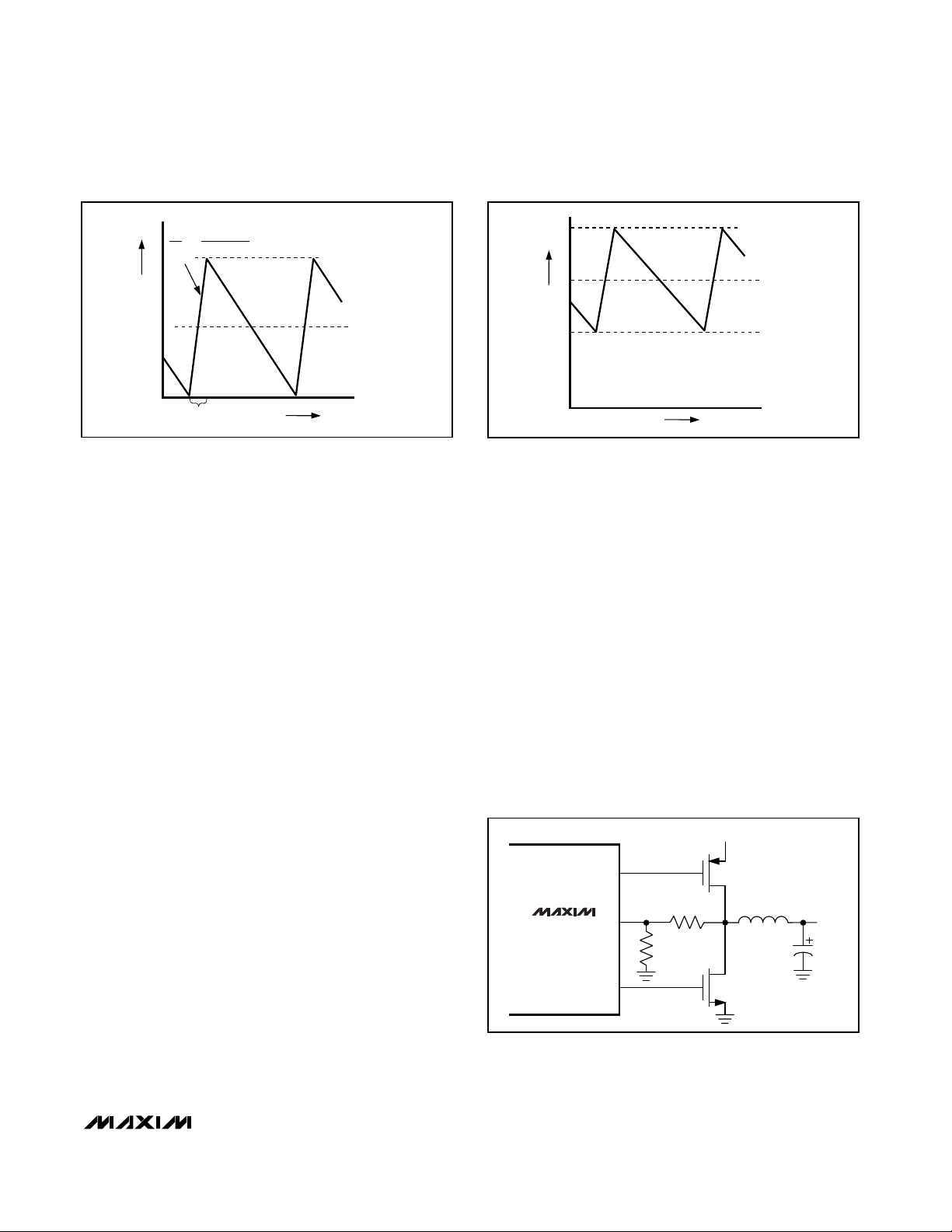
Automatic Pulse-Skipping Switchover
This PWM control algorithm automatically switches over
to pulse-skipping operation at light loads. The
MAX1762/MAX1791 truncates the low-side switch’s ontime when the inductor current drops to zero. The load
current level at which pulse-skipping/PWM crossover
occurs is equal to 1/2 the peak-to-peak ripple current,
which is a function of the inductor value (Figure 6):
The inductor current is never allowed to go negative. If
the output voltage is above its regulation point and the
inductor current reaches zero, the low-side driver is
switched off. Once the output voltage falls below its
regulation point, the high-side driver is switched on.
This causes a dead time in between when the highside and low-side drivers are on, skipping pulses and
resulting in the switching frequency slowing at light
loads, thereby improving efficiency.
MOSFET Gate Drivers
The DH and DL drivers are optimized for driving moderate-size power MOSFETs. This is consistent with the
low duty factor seen in the notebook CPU environment
where a large V
BATT
- V
OUT
differential exists. The highside driver (DH) is rated for 0.6A source/sink capability
and swings from VP to GND. The low-side driver (DL) is
I
KV2LV-V
LOAD(SKIP)
OUT VP OUT
VP
=
×
V
t
tt
ON MIN
ON MIN OFF MAX
()
() ( )
=
µ
µµ
=
+
2.55 s
2.55 s+0.5 s
84%
tK
ON
=×
()
V+0.075V
V
OUT
BATT
Table 3. Operating Frequency
DEVICE
K
(µs)
MIN
TYP
MAX
(kHz)
MAX1762/MAX1791
328
3.349 268.7 298.5
(kHz)
(kHz)
Page 13
MAX1762/MAX1791
High-Efficiency, 10-Pin µMAX, Step-Down
Controllers for Notebooks
______________________________________________________________________________________ 13
rated for +0.5A, -0.9A source/sink capability and
swings from VL to GND.
The internal pulldown transistor that drives DL low is
robust, with a 1Ω typical on-resistance. This helps prevent DL from being pulled up during the fast rise time of
the inductor node, due to capacitive coupling from the
drain to the gate of the low-side synchronous-rectifier
MOSFET. However, for high-current applications, some
combinations of high-and low-side FETS may cause
excessive gate-drain coupling, which can lead to poor
efficiency, EMI, and shoot-through currents.
An adaptive dead-time circuit monitors the DL output
and prevents the high-side FET from turning on until DL
is fully turned off. The dead time at the other edge (DH
turning off) is determined by a fixed 35ns (typ) internal
delay.
Low-Side Current-Limit Sensing (ILIM)
The current-limit circuit employs a unique “valley” current-sensing algorithm that uses the on-state resistance
of the low-side MOSFET as a current-sensing element.
If the current-sense signal is below the current-limit
threshold (-100mV from CS to GND), the PWM is not
allowed to initiate a new cycle (Figure 7). The actual
peak current is greater than the current-limit threshold
by an amount equal to the inductor ripple current.
Therefore, the exact current-limit characteristic and
maximum load capability are a function of the MOSFET
on-resistance, inductor value, and battery voltage.
If greater current-limit accuracy is desired, CS must be
connected to the junction of the low-side switch source
and a current-sense resistor to GND. The current limit
will be 0.1V/R
SENSE
, and the accuracy will be ±10%.
A resistive voltage-divider from the inductor’s switching
mode to ground can be used to adjust the current-limit
sense voltage that appears at CS (Figure 8). Keep the
impedance at this mode low to avoid errors at CS.
POR and Soft-Start
Power-on reset (POR) occurs when V
BATT
rises above
approximately 2V, resetting the fault latch and soft-start
counter and preparing the PWM for operation. UVLO
circuitry inhibits switching until V
VP
rises above 4.1V,
whereupon an internal digital soft-start timer begins to
ramp up the maximum allowed current limit. The ramp
occurs in five steps: 20%, 40%, 60%, 80%, and 100%;
100% current is available after approximately 1.7ms.
Output Undervoltage Protection
The output UVLO function is similar to foldback current
limiting but employs a timer rather than a variable current limit. The output undervoltage protection is
enabled 20ms after POR or when coming out of shutdown. If the output is under 70% of the nominal value,
Figure 6. Pulse-Skipping/Discontinuous Crossover Point
INDUCTOR CURRENT
I
LOAD
= I
PEAK
/2
ON-TIME0 TIME
I
PEAK
L
V
BATT
- V
OUT
∆
i
∆
t
=
Figure 7. “Valley” Current-Limit Threshold Point
INDUCTOR CURRENT
I
LIMIT
I
LOAD
0TIME
I
PEAK
Figure 8. Using a Resistive Voltage-Divider to Adjust CurrentLimit Sense Voltage to 200mV
CS
DH
DL
V
P
MAX1762
MAX1791
1.0kΩ
V
OUT
1.0kΩ
Page 14
MAX1762/MAX1791
High-Efficiency, 10-Pin µMAX, Step-Down
Controllers for Notebooks
14 ______________________________________________________________________________________
then the PWM is latched off and does not restart until
VP power is cycled, or SHDN is toggled low then high.
Design Procedure
Begin by establishing the input voltage range and maximum load current before choosing an inductor and its
associated ripple-current ratio (LIR). The following four
factors dictate the rest of the design:
1) Input voltage range. The maximum value (V
VP
(MAX)
) must accommodate the maximum AC
adapter voltage. The minimum value (V
VP(MIN)
)
must account for the lowest input voltage after
drops due to connectors, fuses, and battery selector switches. If there is a choice at all, lower input
voltages result in better efficiency.
2) Maximum load current. There are two values to
consider. The peak load current (I
LOAD(MAX)
) determines the instantaneous component stress and filtering requirements and thus drives output
capacitor selection, inductor saturation rating, and
the design of the current-limit circuit. The continuous load current (I
LOAD
) determines the thermal
stress and thus drives the selection of input capacitors, MOSFETs, and other critical heat-contributing
components. Modern notebook CPUs generally
exhibit, I
LOAD
= I
LOAD(MAX)
x 0.8.
3) Switching frequency. The MAX1762/MAX1791
have a nominal switching frequency of 300kHz.
4) Inductor ripple-current ratio (LIR). LIR is the ratio
of the peak-to-peak ripple current to the average
inductor current. Size and efficiency trade-offs must
be considered when setting the inductor ripple-current ratio. Low inductor values cause large ripple
currents, resulting in the smallest size but poor efficiency and high output noise. The minimum practical inductor value is one that causes the circuit to
operate at critical conduction (where the inductor
current just touches zero with every cycle). Inductor
values lower than this grant no further size-reduction benefit.
The MAX1762/MAX1791s’ pulse-skipping algorithm initiates skip mode at the critical conduction point. So, the
inductor operating point also determines the load-current value at which switchover occurs. The optimum
point is usually found between 20% and 50% ripple
current.
The inductor ripple current also impacts transientresponse performance, especially at low V
VP
- V
OUT
difference. Low inductor values allow the inductor current to slew faster, replenishing charge removed from
the output filter capacitors by a sudden load step. The
peak amplitude of the output transient (V
SAG
) is also a
function of the maximum duty factor, which can be calculated from the on-time and minimum off-time:
where minimum off-time = 0.5µs (max).
Inductor Selection
The switching frequency (on-time) and operating point
(% ripple or LIR) determine the inductor value as follows:
Example: I
LOAD(MAX)
= 2A, VVP= 7V, V
OUT
= 1.6V, f =
300kHz, 35% ripple current or LIR = 0.35:
Find a low-loss inductor having the lowest possible DC
resistance that fits in the allotted dimensions. Ferrite
cores are often the best choice. The core must be large
enough not to saturate at the peak inductor current
(I
PEAK
):
I
PEAK
= I
LOAD(MAX)
+ [(LIR/2) ✕I
LOAD(MAX)
]
Determining Current Limit
The minimum current-limit threshold must be great
enough to support the maximum load current when the
current limit is at the minimum tolerance value. The valley of the inductor current occurs at I
LOAD(MAX)
minus
half of the ripple current; therefore:
I
VALLEY
> I
LOAD(MAX)
- [(LIR/2) ✕I
LOAD(MAX)
]
where I
VALLEY
= minimum current-limit threshold volt-
age divided by the R
DS(ON)
of Q2. For the MAX1762/
MAX1791, the minimum current-limit threshold is 90mV.
Use the worst-case maximum value for R
DS(ON)
from
the MOSFET Q2 data sheet, and add some margin for
the rise in R
DS(ON)
with temperature. A good general
rule is to allow 0.5% additional resistance for each °C of
temperature rise.
L
kHz A
H=
×××
=
1.6V(7V -1.6V)
7 300 0 35 2
59.. µ
L =
×ƒ× ×
V(V-V)
V LIR I
OUT VP OUT
VP LOAD(MAX)
V
)L
V
V
+t
V-V
V
-t
SAG
LOAD(MAX)
OUT
VP
OFF(MIN)
OUT OUT
VP OUT
VP
OFF(MIN)
2
=
×
××
(∆IK
CVK2
Page 15

MAX1762/MAX1791
High-Efficiency, 10-Pin µMAX, Step-Down
Controllers for Notebooks
______________________________________________________________________________________ 15
Examining the 2A circuit example with a maximum
R
DS(ON)
= 52mΩ at +85°C temperature reveals the fol-
lowing:
I
VALLEY
= 90mV / 52mΩ = 1.73A
Checking the corresponding I
LOAD(MAX) reveals:
A current-sense resistor can be connected from CS to
GND to set the current limit for the device. The
MAX1762/MAX1791 use the sense resistor instead of
the R
DS(ON)
of Q2 to limit the current. The maximum
value of the sense resistor can be calculated with the
equation:
I
LIMIT
= 90mV / R
SENSE
Output Capacitor Selection
The output filter capacitor must have low enough effective series resistance (ESR) to meet output ripple and
load-transient requirements, yet have high enough ESR
to satisfy stability requirements. In CPU V
CORE
converters and other applications where the output is subject
to large load transients, the output capacitor’s size
depends on how much ESR is needed to prevent the
output from dipping too low under a load transient.
Ignoring the sag due to finite capacitance:
where V
DIP
is the maximum tolerable transient voltage
drop. In non-CPU applications, the output capacitor’s
size depends on how much ESR is needed to maintain
an acceptable level of output voltage ripple:
where V
P-P
is the peak-to-peak output voltage ripple.
The actual microfarad capacitance value required
relates to the physical size needed to achieve low ESR,
as well as to the chemistry of the capacitor technology.
Thus, the capacitor is usually selected by ESR and voltage rating rather than by capacitance value (this is true
of tantalum, SP, POS, and other electrolytic-type
capacitors).
When using low-capacity filter capacitors such as
ceramics, capacitor size is usually determined by the
capacity needed to prevent V
SAG
and V
SOAR
from
causing problems during load transients. Generally,
once enough capacitance is added to meet the overshoot requirement, undershoot at the rising load edge
is no longer a problem (see the V
SAG
equation in the
Design Procedure section).
The amount of overshoot due to stored inductor energy
can be calculated as:
where I
PEAK
is the peak inductor current.
Stability Considerations
Stability is determined by the value of the ESR zero
(f
ESR
) relative to the switching frequency (f). The point
of instability is given by the following equation:
where:
For a typical 300kHz application, the ESR zero frequency must be well below 95kHz, preferably below 50kHz.
Tantalum, Sanyo POSCAP, and Panasonic SP capacitors in widespread use at the time of publication have
typical ESR zero frequencies of 20kHz. In the design
example used for inductor selection, the ESR needed
to support a specified ripple voltage is found by the
equation:
where LIR is the inductor ripple current ratio, and I
LOAD
is the average DC load. Using a LIR = 0.35 and an
average load current of 2A, the ESR needed to support
50mV
P-P
ripple is 71mΩ.
Do not use high-value ceramic capacitors directly
across the fast feedback inputs (FB to GND) without
taking precautions to ensure stability. Large ceramic
capacitors can have a high-ESR zero frequency and
cause erratic, unstable operation. However, it is easy to
add enough series resistance by placing the capacitors a couple of inches downstream from the junction of
the inductor and FB pin.
Unstable operation manifests itself in two related but distinctly different ways: double-pulsing and fast-feedback
loop instability. Double pulsing occurs due to noise on
the output or because the ESR is so low that there is not
enough voltage ramp in the output voltage signal. This
R
V
LIR
ESR
RIPPLE(p-p)
LOAD
=
ƒ×I
IJ
×× ×
ESR
ESR OUT
1
2 π RC
IJ
ƒ
ESR
π
∆V
LI
CV
PEAK
2
OUT
≤
2
R
V
LIR I
ESR
P-P
LOAD(MAX)
≤
×
R
V
I
ESR
DIP
LOAD(MAX)
≤
ƒ
I
1- 0.5 LIR
1.73A
1- 0.5 0.35
2.1A
LOAD(MAX)
VALLEY
==×=
I
Page 16

MAX1762/MAX1791
High-Efficiency, 10-Pin µMAX, Step-Down
Controllers for Notebooks
16 ______________________________________________________________________________________
“fools” the error comparator into triggering a new cycle
immediately after the 500ns minimum off-time period has
expired. Double pulsing is more annoying than harmful,
resulting in nothing worse than increased output ripple.
However, it can indicate the possible presence of loop
instability, which is caused by insufficient ESR. Loop
instability can result in oscillations at the output after line
or load perturbations that can cause the output voltage
to fall below the tolerance limit.
The easiest method for checking stability is to apply a
very fast zero-to-max load transient (refer to the
MAX1762/MAX1791 EV kit manual) and carefully
observe the output voltage ripple envelope for overshoot and ringing. It can help to simultaneously monitor
the inductor current with an AC current probe. Do not
allow more than one cycle of ringing after the initial
step-response under- or overshoot.
Input Capacitor Selection
The input capacitor must meet the ripple-current requirement (I
RMS
) imposed by the switching currents.
Nontantalum chemistries (ceramic or OS-CON™) are preferred due to their resilience to power-up surge currents:
Power MOSFET Selection
DC bias and output power considerations dominate the
selection of the power MOSFETs used with the
MAX1762/MAX1791. Take care not to exceed the
device’s maximum voltage ratings. In general, both
switches are exposed to the supply voltage, so select
MOSFETs with VDS(max) greater than VP (max). Gate
drives to the n-channel and p-channel MOSFETs are
not symmetrical. The n-channel device is driven from
ground to the logic supply VL, while the p-channel
device is driven from VP to ground. The maximum rating for VGSfor the n-channel device is usually not an
issue; however, V
GS
(max) for the p-channel must be at
least VP (max). Since V
GS
(max) is usually lower than
V
DS
(max), gate drive constraints often dictate the
required p-channel breakdown rating.
For moderate input-to-output differentials, the high-side
MOSFET (Q1) can be sized smaller than the low-side
MOSFET (Q2) without compromising efficiency. The
high-side switch operates at a very low duty cycle
under these conditions, so most conduction losses
occur in Q2. For maximum efficiency, choose a highside MOSFET (Q1) that has conduction losses (I2R x
duty cycle) equal to the switching losses (CV
VP
2
f).
Make sure that the conduction losses at the minimum
input voltage do not exceed the package thermal limits
or violate the overall thermal budget. Conduction losses
plus switching losses at the maximum input voltage
should not exceed the package ratings or violate the
overall thermal budget (see MOSFET Power Dis-
sipation).
In addition to efficiency considerations, the selection of
the R
DS(ON)
of the low-side MOSFET must account for
the regulator’s required current limit. Choose a MOSFET that has a low enough resistance over the operating temperature range such that the device does not
enter current limit during normal operation (see the
Determining Current Limit section). Conversely, ultralow R
DS(ON)
devices may set the current limit too high
and may result in only incremental improvements in efficiency. Some large n-channel FETs also have substantial interelectrode capacitance. Verify that the
MAX1762/ MAX1791 DL driver can hold the gate off
when the high side switch turns on. Cross-conduction
problems can occur when the high-side switch turns on
due to coupling through the n-channel’s parasitic drainto-gate capacitance.
The MAX1762/MAX1791 have adaptive dead-time circuitry that prevents the high-side and low-side
MOSFETs from conducting at the same time (see MOS-
FET Gate Drivers). Even with this protection, it is still
possible for delays internal to the MOSFET to prevent
one MOSFET from turning off while the other is turned
on. The maximum mismatch time that can be tolerated
is 60ns. Select devices that have low turn-off times, and
make sure that NFET(tD(off,max)) - PFET(tD(on,min)) <
60ns, and PFET(tD(off,max)) - NFET(tD(on,min)) < 60ns.
Failure to do so may result in efficiency-killing shootthrough currents.
MOSFET Power Dissipation
Worst-case conduction losses occur at the duty factor
extremes. For the high-side MOSFET, the worst-case
power dissipation (PD) due to resistance occurs at minimum battery voltage:
Generally, a small high-side MOSFET is desired to
reduce switching losses at high input voltage. However,
the R
DS(ON)
required to stay within package power-dissipation limits often limits how small the MOSFET can
be. Again, the optimum occurs when the switching (AC)
losses equal the conduction (R
DS(ON)
) losses. High-
PD(Q1 resistance)
V
V
IR
OUT
VP(MIN)
LOAD DS(ON)
2
=
××
I
V(V-V)
RMS LOAD
OUT VP OUT
VP
=×
I
V
OS-CON is a trademark of Sanyo.
Page 17

MAX1762/MAX1791
High-Efficiency, 10-Pin µMAX, Step-Down
Controllers for Notebooks
______________________________________________________________________________________ 17
side switching losses do not usually become an issue
until the input is greater than approximately 15V.
Switching losses in the high-side MOSFET can become
an insidious heat problem when maximum battery voltage is applied, due to the squared term in the CV2f
switching loss equation. If the high-side MOSFET chosen for adequate R
DS(ON)
at low battery voltages
becomes extraordinarily hot when subjected to
V
VP(MAX)
, reconsider your choice of high-side MOS-
FET.
Calculating the power dissipation in Q1 due to switching losses is difficult since it must allow for difficult
quantifying factors that influence the turn-on and turnoff times. These factors include the internal gate resistance, gate charge, threshold voltage, source inductance, and PC board layout characteristics. The following switching loss calculation provides only a very
rough estimate and is no substitute for breadboard
evaluation, preferably including a verification using a
thermocouple mounted on Q1:
where C
RSS
is the reverse transfer capacitance of Q1,
and I
GATE
is the peak gate-drive source/sink current.
For the low-side MOSFET, the worst-case power dissipation always occurs at maximum battery voltage:
The absolute worst case for MOSFET power dissipation
occurs under heavy overloads that are greater than
I
LOAD(MAX)
but are not quite high enough to exceed
the current limit and cause the fault latch to trip. To protect against this possibility, the circuit must be overdesigned to tolerate:
I
LOAD
= I
LIMIT(HIGH)
+ (LIR / 2 ) ✕I
LOAD(MAX)
where I
LIMIT(HIGH)
is the maximum valley current
allowed by the current-limit circuit, including threshold
tolerance and on-resistance variation. This means that
the MOSFET must be very well heatsinked. If short-circuit protection without overload protection is enough, a
normal I
LOAD
value can be used for calculating compo-
nent stresses.
During the period when the high-side switch is off, current circulates from ground to the junction of both FETs
and the inductor. As a consequence, the polarity of the
switching node is negative with respect to ground. If
unchanged, this voltage is approximately 0.7V (a diode
drop) at both transition edges while both switches are
off. In between the edges, the low-side switch conducts; the drop is I
L
✕
R
DS(ON)
. If a Schottky clamp is
connected across the low-side switch, the initial and
final voltage drops is reduced, improving efficiency
slightly.
Choose a Schottky diode (D1) having a forward voltage
low enough to prevent the Q2 MOSFET body diode
from turning on during the dead time. As a general rule,
a diode having a DC current rating equal to 1/3 of the
load current is sufficient. This diode is optional and can
be removed if efficiency isn’t critical.
Applications Issues
Dropout Performance
The output voltage adjust range for continuous-conduction operation is restricted by the nonadjustable 500ns
(max) minimum off-time one-shot. When working with
low input voltages, the duty-factor limit must be calculated using worst-case values for on- and off-times.
Manufacturing tolerances and internal propagation
delays introduce an error to the tONK-factor. Also,
keep in mind that transient response performance of
buck regulators operating close to dropout is poor, and
bulk output capacitance must often be added.
Dropout design example: VIN= 7V (min), V
OUT
= 5V, f
= 300kHz. The required duty cycle is :
The worst-case on-time is:
The maximum IC duty factor based on timing constraints of the MAX1762/MAX1792 is:
which meets the required duty cycle. Remember to
include inductor resistance and MOSFET on-state voltage drops (V
SW
) when doing worst-case dropout duty-
factor calculations.
Fixed Output Voltages
The MAX1762/MAX1791 Dual Mode operation allows
the selection of common voltages without requiring
external components (Figure 9). Connect FB to GND for
Duty
t
t+t
ON(MIN)
ON(MIN) OFF(MAX)
==
+
=
218
218 05
082
.
..
.,
µ
µµ
s
ss
t
V+0.075
V
5V+0.075
7V
ON(MIN)
OUT
VP
=×=×
×=
K
ss335 90 218.%.µµ
DC
V+V
V-V
5V+0.1V
7V - 0.1V
REQ
OUT SW
VP SW
===074.
PD(Q2) -
V
V
IR
OUT
VP(MAX)
LOAD DS
2
=
××1
PD (Q1 switching)
CV I
I
RSS VP(MAX) LOAD
GATE
2
=
×׃×
Page 18

MAX1762/MAX1791
High-Efficiency, 10-Pin µMAX, Step-Down
Controllers for Notebooks
18 ______________________________________________________________________________________
a fixed +1.8V (MAX1762) or 3.3V (MAX1791) output.
Connect FB to VL for a fixed 2.5V (MAX1762) or 5.0V
(MAX1791) output. Otherwise, connect FB to a resistive
voltage-divider for an adjustable output.
Setting the Output Voltage
Select V
OUT
> 1.25V for the MAX1762/MAX1791 by
connecting FB to a resistive voltage-divider between
V
OUT
and GND (Figure 2). Choose R2 to be about
10kΩ, and solve for R1 using the equation:
where V
FB
= 1.25V. For a V
OUT
= 3.0V, R2 = 10kΩ and
R1 = 14kΩ.
For a desired V
OUT
< 1.25V, connect FB to a resistive
voltage-divider between REF and OUT (Figure 3).
Choose R1 to be about 50kΩ, and solve for R2 using
the equation:
where V
FB
= 1.25V and V
REF
= 2.0V. For a V
OUT
=
1.0V, R1 = 50kΩ and R2 = 16.5kΩ. Under these condi-
tions, a minimum load of V
REF
- VFB/ R1 >15µA is
required.
PC Board Layout Guidelines
Careful PC board layout is critical to achieve low
switching losses and clean, stable operation. This is
especially true when multiple converters are on the
same PC board where one circuit can affect the other.
The switching power stages require particular attention
(Figure 10). Refer to the MAX1791 EV kit manual for a
specific layout example.
If possible, mount all of the power components on the
top side of the board, with their ground terminals flush
against one another. Follow these guidelines for good
PC board layout:
• Isolate the power components on the top side from
the sensitive analog components on the bottom
side with a ground shield. Use a separate GND
plane under OUT. Avoid the introduction of AC currents into the GND ground planes. Run the power
plane ground currents on the top side only, if possible.
• Keep the high-current paths short, especially at the
ground terminals. This practice is essential for stable, jitter-free operation.
• Keep the power traces and load connections short.
This practice is essential for high efficiency. Using
thick copper PC boards (2oz vs. 1oz) can enhance
full-load efficiency by 1% or more. Correctly routing
PC board traces is a difficult task that must be
approached in terms of fractions of centimeters,
where a single milliohm of excess trace resistance
causes a measurable efficiency penalty.
• Inductor and GND connections to the synchronous
rectifiers for current limiting must be made using
Kelvin sensed connections to guarantee the current-limit accuracy. With 8-pin SO MOSFETs, this is
best done by routing power to the MOSFETs from
outside using the top copper layer, while connecting GND and CS inside (underneath) the µMAX
package.
• When trade-offs in trace lengths must be made, it’s
preferable to allow the inductor charging path to be
made longer than the discharge path. For example,
it’s better to allow some extra distance between the
input capacitors and the high-side MOSFET than to
allow distance between the inductor and the lowside MOSFET or between the inductor and the output filter capacitor.
• Ensure that the OUT connection to C
OUT
is short
and direct. However, in some cases it may be desirable to deliberately introduce some trace length
between the OUT connector node and the output
filter capacitor (see Stability Considerations).
• Route high-speed switching nodes (CS, DH, and
DL) away from sensitive analog areas (FB). Use
GND as an EMI shield to keep radiated switching
noise away from the IC’s feedback divider and analog bypass capacitors.
R2
V-V
V-V
R1
OUT FB
FB REF
=
×
VV
R1
R2
OUT FB
=ƒ × +
1
Figure 9. Feedback MUX
MAX1762
TO ERROR
AMP
0.150V
2.5V
FB
FIXED
1.8V
FIXED
3.3V
OUT
Page 19

MAX1762/MAX1791
High-Efficiency, 10-Pin µMAX, Step-Down
Controllers for Notebooks
______________________________________________________________________________________ 19
Layout Procedure
1) Place the power components first, with ground terminals adjacent (Q1 source, CIN, C
OUT
). If possible, make all these connections on the top layer
with wide, copper-filled areas.
2) Mount the controller IC adjacent to the synchronous-rectifier MOSFETs, preferably on the back
side in order to keep CS, GND, and the DL gate
drive lines short and wide. The DL gate trace must
be short and wide (measuring 50mils to 100mils
wide if the MOSFET is 1in from the controller IC).
3) Place the V
L
bypass capacitor near the controller
IC.
4) Make the DC-DC controller ground connections as
follows: Near the IC, create a small analog ground
plane. Connect this plane to GND, and use this
plane for the ground connection for the REF and
V
VP
bypass capacitors and FB dividers.
5) On the board’s top side (power planes), make a
star ground to minimize crosstalk between the two
sides. The top-side star ground is a star connection
of the input capacitors, side 1 low-side MOSFET.
Keep the resistance low between the star ground
and the source of the low-side MOSFETs for accurate current limit. Connect the top-side star ground
(used for MOSFET, input, and output capacitors) to
the small island with a single short, wide connection
(preferably just a via).
6) Connect the output power planes directly to the output filter capacitor positive and negative terminals
with multiple vias.
Chip Information
TRANSISTOR COUNT: 3520
PROCESS: S8E1FP
Figure 10. PC Board Layout Example
AGND
PGND
USE AGND PLANE TO:
- BYPASS V
CC
AND REF
- TERMINATE EXTERNAL FB
DIVIDER (IF USED)
- PIN-STRAP CONTROL
INPUTS
USE PGND PLANE TO:
- BYPASS V
VP
- CONNECT PGND TO THE TOPSIDE STAR GROUND
VIA TO GROUND
NOTE
: EXAMPLE SHOWN IS FOR DUAL n-CHANNEL MOSFET.
CONNECT PGND TO AGND
BENEATH THE MAX1762/MAX1791 AT
ONE POINT ONLY AS SHOWN.
GND
P1
N1
VOUT
VL
VBATT
L1
C2
C1
D1
Page 20

MAX1762/MAX1791
High-Efficiency, 10-Pin µMAX, Step-Down
Controllers for Notebooks
Maxim cannot assume responsibility for use of any circuitry other than circuitry entirely embodied in a Maxim product. No circuit patent licenses are
implied. Maxim reserves the right to change the circuitry and specifications without notice at any time.
20 ____________________Maxim Integrated Products, 120 San Gabriel Drive, Sunnyvale, CA 94086 408-737-7600
© 2005 Maxim Integrated Products Printed USA is a registered trademark of Maxim Integrated Products, Inc.
Package Information
10LUMAX.EPS
PACKAGE OUTLINE, 10L uMAX/uSOP
1
1
21-0061
REV.DOCUMENT CONTROL NO.APPROVAL
PROPRIETARY INFORMATION
TITLE:
TOP VIEW
FRONT VIEW
1
0.498 REF
0.0196 REF
S
6°
SIDE VIEW
α
BOTTOM VIEW
0° 0° 6°
0.037 REF
0.0078
MAX
0.006
0.043
0.118
0.120
0.199
0.0275
0.118
0.0106
0.120
0.0197 BSC
INCHES
1
10
L1
0.0035
0.007
e
c
b
0.187
0.0157
0.114
H
L
E2
DIM
0.116
0.114
0.116
0.002
D2
E1
A1
D1
MIN
-A
0.940 REF
0.500 BSC
0.090
0.177
4.75
2.89
0.40
0.200
0.270
5.05
0.70
3.00
MILLIMETERS
0.05
2.89
2.95
2.95
-
MIN
3.00
3.05
0.15
3.05
MAX
1.10
10
0.6±0.1
0.6±0.1
Ø0.50±0.1
H
4X S
e
D2
D1
b
A2
A
E2
E1
L
L1
c
α
GAGE PLANE
A2 0.030 0.037 0.75 0.95
A1
 Loading...