

Page 1
General Description
The MAX1777/MAX1977/MAX1999 dual step-down,
switch-mode power-supply (SMPS) controllers generate
logic-supply voltages in battery-powered systems. The
MAX1777/MAX1977/MAX1999 include two pulse-width
modulation (PWM) controllers, adjustable from 2V to 5.5V
or fixed at 5V and 3.3V. These devices feature two linear
regulators providing 5V and 3.3V always-on outputs.
Each linear regulator provides up to 100mA output current with automatic linear regulator bootstrapping to the
main SMPS outputs. The MAX1777/MAX1977/MAX1999
include on-board power-up sequencing, a power-good
(PGOOD) output, digital soft-start, and internal soft-stop
output discharge that prevents negative voltages on shutdown.
Maxim’s proprietary Quick-PWM™ quick-response, constant on-time PWM control scheme operates without
sense resistors and provides 100ns response to load
transients while maintaining a relatively constant switching frequency. The unique ultrasonic pulse-skipping
mode maintains the switching frequency above 25kHz,
which eliminates noise in audio applications. Other features include pulse skipping, which maximizes efficiency
in light-load applications, and fixed-frequency PWM
mode, which reduces RF interference in sensitive applications.
The MAX1777 features a 200kHz/5V and 300kHz/3.3V
SMPS for highest efficiency, while the MAX1977 features
a 400kHz/5V and 500kHz/3.3V SMPS for “thin and light”
applications. The MAX1999 provides a pin-selectable
switching frequency, allowing either 200kHz/300kHz or
400kHz/500kHz operation of the 5V/3.3V SMPSs, respectively. The MAX1777/MAX1977/MAX1999 are available in
28-pin QSOP packages and operate over the extended
temperature range (-40°C to +85°C). The MAX1777/
MAX1977/MAX1999 are available in lead-free packages.
Applications
Notebook and Subnotebook Computers
PDAs and Mobile Communication Devices
3- and 4-Cell Li+ Battery-Powered Devices
Features
♦ No Current-Sense Resistor Needed (MAX1999)
♦ Accurate Current Sense with Current-Sense
Resistor (MAX1777/MAX1977)
♦ 1.5% Output Voltage Accuracy
♦ 3.3V and 5V 100mA Bootstrapped Linear
Regulators
♦ Internal Soft-Start and Soft-Stop Output
Discharge
♦ Quick-PWM with 100ns Load Step Response
♦ 3.3V and 5V Fixed or Adjustable Outputs
(Dual Mode™)
♦ 4.5V to 24V Input Voltage Range
♦ Ultrasonic Pulse-Skipping Mode (25kHz min)
♦ Power-Good (PGOOD) Signal
♦ Overvoltage Protection Enable/Disable
MAX1777/MAX1977/MAX1999
High-Efficiency, Quad Output, Main Power-
Supply Controllers for Notebook Computers
________________________________________________________________ Maxim Integrated Products 1
Ordering Information
19-2187; Rev 1; 9/04
For pricing, delivery, and ordering information, please contact Maxim/Dallas Direct! at
1-888-629-4642, or visit Maxim’s website at www.maxim-ic.com.
PART
TEMP RANGE
PIN-
5V/3V
SWITCHING
FREQUENCY
MAX1777EEI
200k H z/300kH z
MAX1777EEI+
200k H z/300kH z
MAX1977EEI
400k H z/500kH z
MAX1977EEI+
400k H z/500kH z
MAX1999EEI
200k H z/300kH z or
400k H z/500kH z
MAX1999EEI+
200k H z/300kH z or
400k H z/500kH z
Quick-PWM and Dual Mode are trademarks of Maxim
Integrated Products, Inc.
28
27
26
25
24
23
22
21
20
19
18
17
16
15
1
2
3
4
5
6
7
8
9
10
11
12
13
14
BST3
LX3
DH3
LDO3
DL3
GND
LX5
OUT3
OUT5
V+
DL5
LDO5
V
CC
DH5
BST5
TON
ILIM5
FB5
REF
FB3
ILIM3
ON5
ON3
PGOOD
N.C.
QSOP
TOP VIEW
MAX1999
SHDN
PRO
SKIP
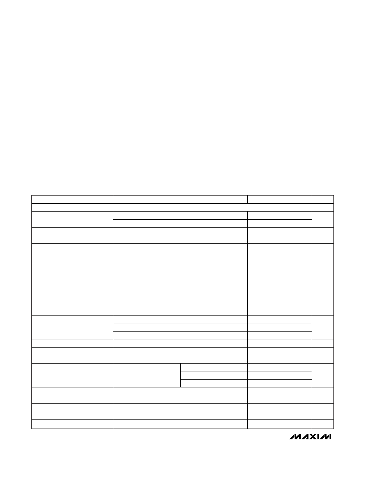
Pin Configurations
Pin Configurations continued at end of data sheet.
+Denotes lead-free package.
PACKAGE
-40°C to +85°C 28 QSOP
-40°C to +85°C 28 QSOP
-40°C to +85°C 28 QSOP
-40°C to +85°C 28 QSOP
-40°C to +85°C 28 QSOP
-40°C to +85°C 28 QSOP
Page 2
MAX1777/MAX1977/MAX1999
High-Efficiency, Quad Output, Main PowerSupply Controllers for Notebook Computers
2 _______________________________________________________________________________________
ABSOLUTE MAXIMUM RATINGS
ELECTRICAL CHARACTERISTICS
(Circuit of Figure 1 and Figure 2, no load on LDO5, LDO3, OUT3, OUT5, and REF, V+ = 12V, ON3 = ON5 = VCC, V
SHDN
= 5V,
T
A
= 0°C to +85°C, unless otherwise noted. Typical values are at TA= +25°C.)
Stresses beyond those listed under “Absolute Maximum Ratings” may cause permanent damage to the device. These are stress ratings only, and functional
operation of the device at these or any other conditions beyond those indicated in the operational sections of the specifications is not implied. Exposure to
absolute maximum rating conditions for extended periods may affect device reliability.
V+, SHDN to GND..................................................-0.3V to +25V
BST_ to GND..........................................................-0.3V to +30V
LX_ to BST_..............................................................-6V to +0.3V
CS_ to GND (MAX1777/MAX1977 only)......................-2V to +6V
V
CC
, LDO5, LDO3, OUT3, OUT5, ON3, ON5, REF,
FB3, FB5, SKIP, PRO, PGOOD to GND ...............-0.3V to +6V
DH3 to LX3..............................................-0.3V to (V
BST3
+ 0.3V)
DH5 to LX5..............................................-0.3V to (V
BST5
+ 0.3V)
ILIM3, ILIM5 to GND...................................-0.3V to (V
CC
+ 0.3V)
DL3, DL5 to GND....................................-0.3V to (V
LDO5
+ 0.3V)
TON to GND (MAX1999 only)...................................-0.3V to +6V
LDO3, LDO5, REF Short Circuit to GND ....................Momentary
LDO3 Current (Internal Regulator) Continuous..............+100mA
LDO3 Current (Switched Over to OUT3) Continuous.....+200mA
LDO5 Current (Internal Regulator) Continuous..............+100mA
LDO5 Current (Switched Over to OUT5) Continuous.....+200mA
Continuous Power Dissipation
28-Pin QSOP (derate 10.8mW/°C above +70°C).........860mW
Operating Temperature Range ...........................-40°C to +85°C
Junction Temperature......................................................+150°C
Storage Temperature Range.............................-65°C to +150°C
Lead Temperature (soldering, 10s).................................+300°C
PARAMETER CONDITIONS
MIN
TYP
MAX
UNITS
MAIN SMPS CONTROLLERS
LDO5 in regulation 6 24
V+ Input Voltage Range
V+ = LDO5, V
OUT5
< 4.43V 4.5 5.5
V
3.3V Output Voltage in
Fixed Mode
V+ = 6V to 24V, FB3 = GND, V
SKIP
= 5V
V
V+ = 6V to 24V, FB5 = GND, V
SKIP
= 5V,
MAX1777/MAX1999 (TON = V
CC
)
V+ = 7V to 24V, FB5 = GND, V
SKIP
= 5V,
MAX1977/MAX1999 (TON = GND)
V
Output Voltage in
Adjustable Mode
V+ = 6V to 24V, either SMPS
V
Output Voltage Adjust Range Either SMPS 2.0 5.5 V
FB3, FB5 Adjustable-Mode
Threshold Voltage
Dual-mode comparator 0.1 0.2 V
Either SMPS, V
SKIP
= 5V, 0 to 5A
Either SMPS, SKIP = GND, 0 to 5A
DC Load Regulation
Either SMPS, V
SKIP
= 2V, 0 to 5A
%
Line Regulation Either SMPS, 6V < V+ < 24V
%/V
Current-Limit Threshold
(Positive, Default)
ILIM_ = VCC, GND - CS_ (MAX1777/MAX1977),
GND - LX_ (MAX1999)
93
107 mV
V
ILIM_
= 0.5V 40 50 60
V
ILIM_
= 1V 93
107
Current-Limit Threshold
(Positive, Adjustable)
GND - CS_
(MAX1777/MAX1977),
GND - LX_ (MAX1999)
V
ILIM_
= 2V
215
mV
Zero-Current Threshold
SKIP = GND, ILIM_ = V
CC
, GND - CS_
(MAX1777/MAX1977), GND - LX_ (MAX1999)
3mV
Current-Limit Threshold
(Negative, Default)
SKIP = ILIM_ = VCC, GND - CS_ (MAX1777/MAX1977),
GND - LX_ (MAX1999)
mV
Soft-Start Ramp Time Zero to full limit 1.7 ms
3.285 3.330 3.375
5V Output Voltage in Fixed Mode
4.975 5.050 5.125
1.975 2.00 2.025
0.005
185 200
-120
-0.1
-1.5
-1.7
100
100
Page 3
MAX1777/MAX1977/MAX1999
High-Efficiency, Quad Output, Main Power-
Supply Controllers for Notebook Computers
_______________________________________________________________________________________ 3
ELECTRICAL CHARACTERISTICS (continued)
(Circuit of Figure 1 and Figure 2, no load on LDO5, LDO3, OUT3, OUT5, and REF, V+ = 12V, ON3 = ON5 = VCC, V
SHDN
= 5V,
T
A
= 0°C to +85°C, unless otherwise noted. Typical values are at TA= +25°C.)
PARAMETER CONDITIONS
UNITS
5V SMPS
MAX1777 or MAX1999
(V
TON
= 5V), SKIP = V
CC
3.3V SMPS
5V SMPS
MAX1977 or MAX1999
(V
TON
= 0), SKIP = V
CC 3.3V SMPS
Operating Frequency
SKIP = REF 25 36
kHz
V
OUT5
= 5.05V
MAX1777 or MAX1999
(V
TON
= 5V)
V
OUT3
= 3.33V
V
OUT5
= 5.05V
On-Time Pulse Width
MAX1977 or MAX1999
(V
TON
= 0)
V
OUT3
= 3.33V
µs
Minimum Off-Time
350 ns
V
OUT5
= 5.05V 94
MAX1777 or MAX1999
(V
TON
= 5V)
V
OUT3
= 3.33V 91
V
OUT5
= 5.05V 88
Maximum Duty Cycle
MAX1977 or MAX1999
(V
TON
= 0)
V
OUT3
= 3.33V 85
%
INTERNAL REGULATOR AND REFERENCE
LDO5 Output Voltage
V
LDO5 Short-Circuit Current LDO5 = GND
mA
LDO5 Undervoltage Lockout
Fault Threshold
Falling edge of LDO5, hysteresis = 1% 3.7 4.0 4.3 V
LDO5 Bootstrap Switch Threshold
Falling edge of OUT5, rising edge at OUT5 regulation
point
V
LDO5 Bootstrap
Switch Resistance
LDO5 to OUT5, V
OUT5
= 5V 1.4 3.2 Ω
LDO3 Output Voltage
V
LDO3 Short-Circuit Current LDO3 = GND
mA
LDO3 Bootstrap Switch Threshold
Falling edge of OUT3, rising edge at OUT3 regulation
point
V
LDO3 Bootstrap Switch
Resistance
LDO3 to OUT3, V
OUT3
= 3.2V 1.5 3.5 Ω
REF Output Voltage No external load
V
REF Load Regulation 0 < I
LOAD
< 50µA 10 mV
REF Sink Current REF in regulation 10 µA
V+ Operating Supply Current LDO5 switched over to OUT5, 5V SMPS 25 50 µA
V+ Standby Supply Current V+ = 6V to 24V, both SMPSs off, includes I
SHDN
250 µA
V+ Shutdown Supply Current V+ = 4.5V to 24V 6 15 µA
Quiescent Power Consumption
Both SMPSs on, FB3 = FB5 = SKIP = GND, V
OUT3
=
3.5V, V
OUT5
= 5.3V
3 4.5 mW
FAULT DETECTION
Overvoltage Trip Threshold FB3 or FB5 with respect to nominal regulation point +8
+14 %
ON3 = ON5 = GND, 6V < V+ < 24V, 0 < I
ON3 = ON5 = GND, 6V < V+ < 24V, 0 < I
< 100mA 4.90 5.00 5.10
LDO5
< 100mA 3.28 3.35 3.42
LDO3
MIN TYP MAX
200
300
400
500
1.895 2.105 2.315
0.833 0.925 1.017
0.895 1.052 1.209
0.475 0.555 0.635
250 300
4.43 4.56 4.69
2.80 2.91 3.02
1.980 2.000 2.020
190
180
150
+11
Page 4
MAX1777/MAX1977/MAX1999
High-Efficiency, Quad Output, Main PowerSupply Controllers for Notebook Computers
4 _______________________________________________________________________________________
ELECTRICAL CHARACTERISTICS (continued)
(Circuit of Figure 1 and Figure 2, no load on LDO5, LDO3, OUT3, OUT5, and REF, V+ = 12V, ON3 = ON5 = VCC, V
SHDN
= 5V,
T
A
= 0°C to +85°C, unless otherwise noted. Typical values are at TA= +25°C.)
PARAMETER CONDITIONS
UNITS
Overvoltage Fault
Propagation Delay
FB3 or FB5 delay with 50mV overdrive 10 µs
PGOOD Threshold
FB3 or FB5 with respect to nominal output, falling edge,
typical hysteresis = 1%
-12
-7 %
PGOOD Propagation Delay Falling edge, 50mV overdrive 10 µs
PGOOD Output Low Voltage I
SINK
= 4mA 0.3 V
PGOOD Leakage Current High state, forced to 5.5V 1 µA
Thermal Shutdown Threshold
o
C
Output Undervoltage
Shutdown Threshold
FB3 or FB5 with respect to nominal output voltage 65 70 75 %
Output Undervoltage
Shutdown Blanking Time
From ON_ signal 10 22 35 ms
INPUTS AND OUTPUTS
Feedback Input Leakage Current
V
FB3
= V
FB5
= 2.2V
nA
Low level 0.6
PRO Input Voltage
High level 1.5
V
Low level 0.8
Float level 1.7 2.3SKIP Input Voltage
High level 2.4
V
Low level 0.8
TON Input Voltage
High level 2.4
V
Clear fault level/SMPS off level 0.8
Delay start level 1.7 2.3ON3, ON5 Input Voltage
SMPS on level 2.4
V
V
PRO
or V
TON
= 0 or 5V -1 +1
V
ON_
= 0 or 5V -2 +2
V
SKIP
= 0 or 5V -1 +1
V
SHDN
= 0 or 24V -1 +1
V
CS_
= 0 or 5V -2 +2
Input Leakage Current
V
ILIM3
, V
ILIM5
= 0 or 2V
µA
Rising edge 1.2 1.6 2.0
SHDN Input Trip Level
Falling edge
V
DH_ Gate-Driver
Sink/Source Current
DH3, DH5 forced to 2V 2 A
DL_ Gate-Driver Source Current DL3 (source), DL5 (source), forced to 2V 1.7 A
DL_ Gate-Driver Sink Current DL3 (sink), DL5 (sink), forced to 2V 3.3 A
DH_ Gate-Driver On-Resistance BST - LX_ forced to 5V 1.5 4.0 Ω
DL_, high state (pullup) 2.2 5.0
DL_ Gate-Driver On-Resistance
DL_, low state (pulldown) 0.6 1.5
Ω
MIN TYP MAX
-9.5
160
-200 +40 +200
-0.2 +0.2
0.96 1.00 1.04
Page 5
MAX1777/MAX1977/MAX1999
High-Efficiency, Quad Output, Main Power-
Supply Controllers for Notebook Computers
_______________________________________________________________________________________ 5
ELECTRICAL CHARACTERISTICS (continued)
(Circuit of Figure 1 and Figure 2, no load on LDO5, LDO3, OUT3, OUT5, and REF, V+ = 12V, ON3 = ON5 = VCC, V
SHDN
= 5V,
T
A
= 0°C to +85°C, unless otherwise noted. Typical values are at TA= +25°C.)
PARAMETER CONDITIONS
MIN
TYP
MAX
UNITS
OUT3, OUT5 Discharge-Mode
On-Resistance
12 40 Ω
OUT3, OUT5 Discharge-Mode
Synchronous Rectifier
Turn-On Level
0.2 0.3 0.4 V
ELECTRICAL CHARACTERISTICS
(Circuit of Figure 1 and Figure 2, no load on LDO5, LDO3, OUT3, OUT5, and REF, V+ = 12V, ON3 = ON5 = VCC, V
SHDN
= 5V,
T
A
= -40°C to +85°C, unless otherwise noted.) (Note 1)
PARAMETER CONDITIONS
UNITS
MAIN SMPS CONTROLLERS
LDO5 in regulation 6 24
V+ Input Voltage Range
V+ = LDO5, V
OUT5
< 4.41V 4.5 5.5
V
3.3V Output Voltage in
Fixed Mode
V+ = 6V to 24V, FB3 = GND, V
SKIP
= 5V
V
V+ = 6V to 24V, FB5 = GND, V
SKIP
= 5V,
MAX1777/MAX1999 (TON = V
CC
)
5V Output Voltage in Fixed Mode
V+ = 7V to 24V, FB5 = GND, V
SKIP
= 5V,
MAX1977/MAX1999 (TON = GND)
V
Output Voltage in
Adjustable Mode
V+ = 6V to 24V, either SMPS
V
Output Voltage Adjust Range Either SMPS 2.0 5.5 V
FB3, FB5 Adjustable-Mode
Threshold Voltage
Dual-mode comparator 0.1 0.2 V
Current-Limit Threshold
(Positive, Default)
ILIM_ = VCC, GND - CS_ (MAX1777/MAX1977),
GND - LX_ (MAX1999)
90 110 mV
V
ILIM_
= 0.5V 40 60
V
ILIM_
= 1V 90 110
Current-Limit Threshold
(Positive, Adjustable)
GND - CS_
(MAX1777/MAX1977),
GND - LX_ (MAX1999)
V
ILIM_
= 2V
220
mV
V
OUT5
= 5.05V
MAX1777 or MAX1999
(V
TON
= 5V)
V
OUT3
= 3.33V
V
OUT5
= 5.05V
On-Time Pulse Width
MAX1977 or MAX1999
(V
TON
= 0)
V
OUT3
= 3.33V
µs
Minimum Off-Time
400 ns
INTERNAL REGULATOR AND REFERENCE
LDO5 Output Voltage
V
LDO5 Undervoltage
Lockout Fault Threshold
Falling edge of LDO5, hysteresis = 1% 3.7 4.3 V
ON3 = ON5 = GND, 6V < V+ < 24V, 0 < I
< 100mA 4.90 5.10
LDO5
MIN TYP MAX
3.27 3.39
4.95 5.15
1.97 2.03
180
1.895 2.315
0.833 1.017
0.895 1.209
0.475 0.635
200
Page 6
MAX1777/MAX1977/MAX1999
High-Efficiency, Quad Output, Main PowerSupply Controllers for Notebook Computers
6 _______________________________________________________________________________________
ELECTRICAL CHARACTERISTICS (continued)
(Circuit of Figure 1 and Figure 2, no load on LDO5, LDO3, OUT3, OUT5, and REF, V+ = 12.0.V, ON3 = ON5 = VCC, V
SHDN
= 5V,
T
A
= -40°C to +85°C, unless otherwise noted.) (Note 1)
PARAMETER CONDITIONS
UNITS
LDO5 Bootstrap Switch Threshold
Falling edge of OUT5, rising edge at OUT5 regulation
point
V
LDO5 Bootstrap
Switch Resistance
LDO5 to OUT5, V
OUT5
= 5V 3.2 Ω
LDO3 Output Voltage
V
LDO3 Bootstrap Switch Threshold
Falling edge of OUT3, rising edge at OUT3 regulation
point
V
LDO3 Bootstrap
Switch Resistance
LDO3 to OUT3, V
OUT3
= 3.2V 3.5 Ω
REF Output Voltage No external load
V
REF Load Regulation 0 < I
LOAD
< 50µA 10 mV
REF Sink Current REF in regulation 10 µA
V+ Operating Supply Current LDO5 switched over to OUT5, 5V SMPS 50 µA
V+ Standby Supply Current V+ = 6V to 24V, both SMPSs off, includes I
SHDN
300 µA
V+ Shutdown Supply Current V+ = 4.5V to 24V 15 µA
Quiescent Power Consumption
Both SMPSs on, FB3 = FB5 = SKIP = GND, V
OUT3
=
3.5V, V
OUT5
= 5.3V
4.5 mW
FAULT DETECTION
Overvoltage Trip Threshold FB3 or FB5 with respect to nominal regulation point +8 +14 %
PGOOD Threshold
FB3 or FB5 with respect to nominal output, falling edge,
typical hysteresis = 1%
-12 -7 %
PGOOD Output Low Voltage I
SINK
= 4mA 0.3 V
PGOOD Leakage Current High state, forced to 5.5V 1 µA
Output Undervoltage
Shutdown Threshold
FB3 or FB5 with respect to nominal output voltage 65 75 %
Output Undervoltage
Shutdown Blanking Time
From ON_ signal 10 40 ms
INPUTS AND OUTPUTS
Feedback Input Leakage Current
V
FB3
= V
FB5
= 2.2V
nA
Low level 0.6
PRO Input Voltage
High level 1.5
V
Low level 0.8
Float level 1.7 2.3
SKIP Input Voltage
High level 2.4
V
Low level 0.8
TON Input Voltage
High level 2.4
V
MIN TYP MAX
4.43 4.69
ON3 = ON5 = GND, 6V < V+ < 24V, 0 < I
< 100mA 3.27 3.43
LDO3
2.80 3.02
1.975 2.025
-200 +200
Page 7
MAX1777/MAX1977/MAX1999
High-Efficiency, Quad Output, Main Power-
Supply Controllers for Notebook Computers
_______________________________________________________________________________________ 7
ELECTRICAL CHARACTERISTICS (continued)
(Circuit of Figure 1 and Figure 2, no load on LDO5, LDO3, OUT3, OUT5, and REF, V+ = 12.0.V, ON3 = ON5 = VCC, V
SHDN
= 5V,
T
A
= -40°C to +85°C, unless otherwise noted.) (Note 1)
PARAMETER CONDITIONS
MIN
TYP
MAX
UNITS
Clear fault level/SMPS off level 0.8
Delay start level 1.7 2.3ON3, ON5 Input Voltage
SMPS on level 2.4
V
V
PRO
or V
TON
= 0 or 5V -1 +1
V
ON_
= 0 or 5V -1 +1
V
SKIP
= 0 or 5V -2 +2
V
SHDN
= 0 or 24V -1 +1
V
CS_
= 0 or 5V -2 +2
Input Leakage Current
V
ILIM3
, V
ILIM5
= 0 or 2V
µA
Rising edge 1.2 2.0
SHDN Input Trip Level
Falling edge
V
DH_ Gate-Driver On-Resistance BST - LX_ forced to 5V 4.0 Ω
DL_, high state (pullup) 5.0
DL_ Gate-Driver On-Resistance
DL_, low state (pulldown) 1.5
Ω
OUT3, OUT5 Discharge-Mode
On-Resistance
40 Ω
OUT3, OUT5 Discharge-Mode
Synchronous Rectifier
Turn-On Level
0.2 0.4 V
Note 1: Specifications to -40°C are guaranteed by design, not production tested.
-0.2 +0.2
0.96 1.04
Page 8
MAX1777/MAX1977/MAX1999
High-Efficiency, Quad Output, Main PowerSupply Controllers for Notebook Computers
8 _______________________________________________________________________________________
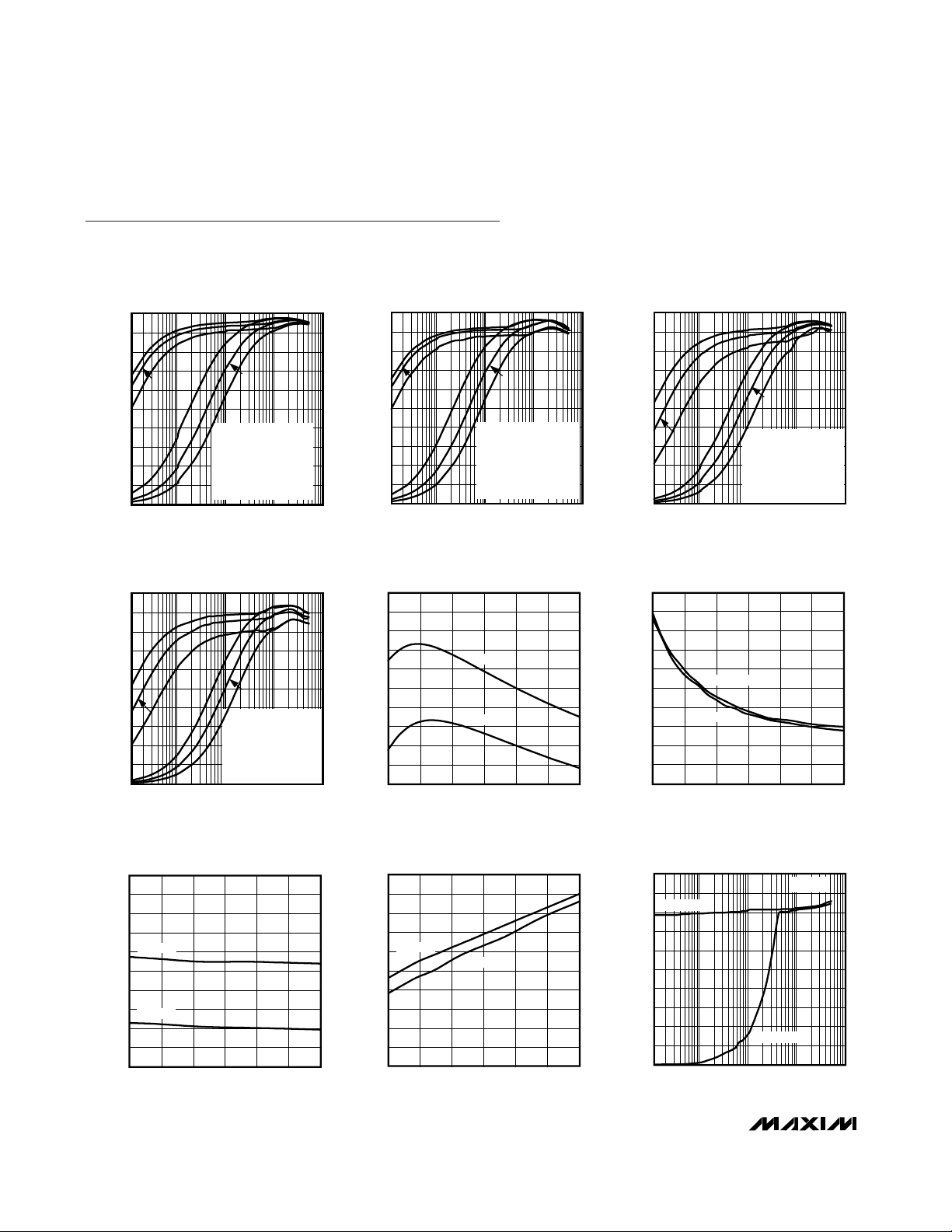
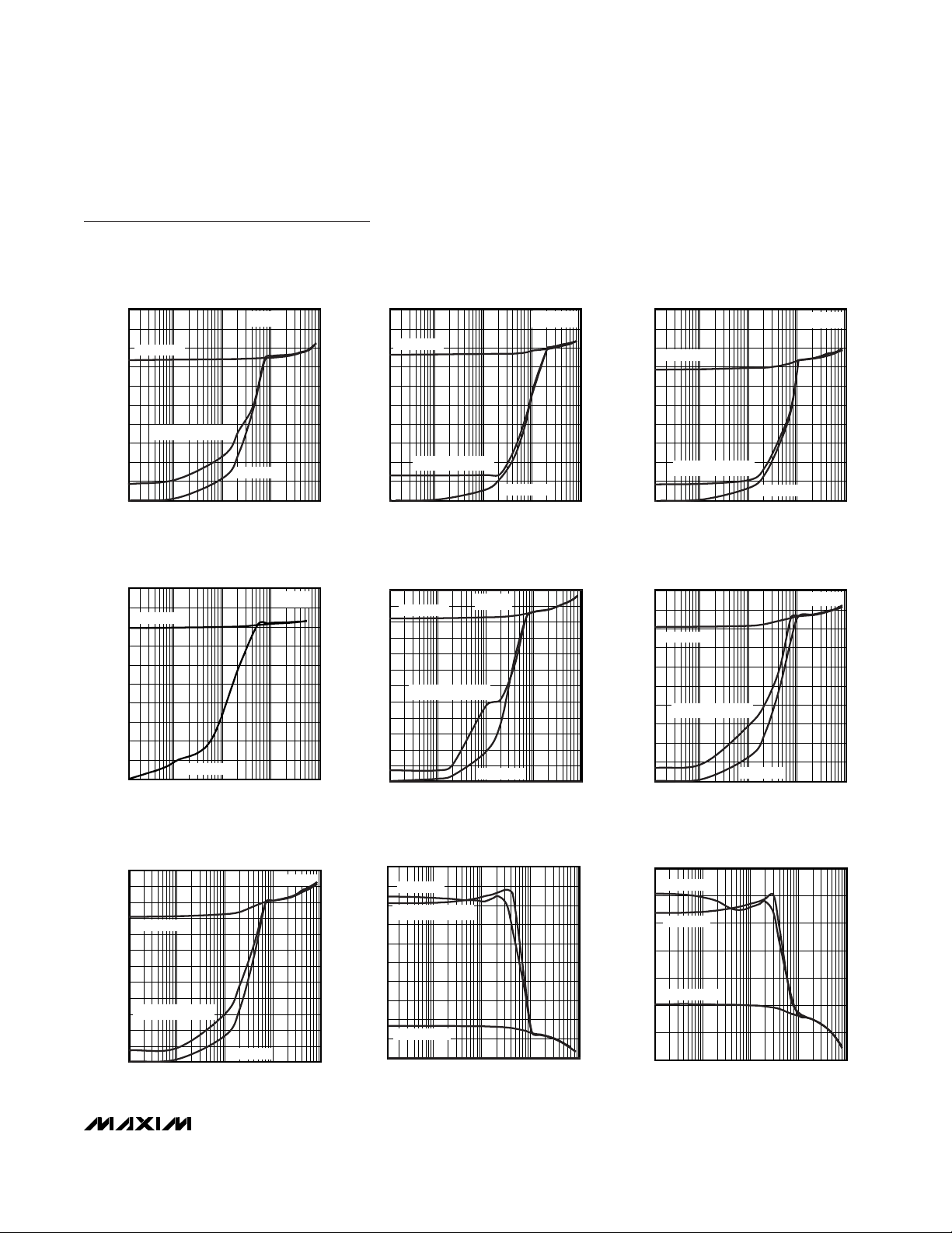
Typical Operating Characteristics
(Circuit of Figure 1 and Figure 2, no load on LDO5, LDO3, OUT3, OUT5, and REF, V+ = 12V, ON3 = ON5 = VCC, SHDN = V+,
R
CS
= 7mΩ, V
ILIM
_ = 0.5V, TA= +25°C, unless otherwise noted.)
100
0
0.001 0.01 0.1 1 10
5V OUTPUT EFFICIENCY
vs. LOAD CURRENT (MAX1777)
20
MAX1777 toc01
LOAD CURRENT (A)
EFFICIENCY (%)
40
60
80
70
50
30
10
90
A: IDLE MODE, VIN = 7V
B: IDLE MODE, V
IN
= 12V
C: IDLE MODE, V
IN
= 24V
D: PWM MODE, V
IN
= 7V
E: PWM MODE, V
IN
= 12V
F: PWM MODE, V
IN
= 24V
A
B
C
D
E
F
100
0
0.001 0.01 0.1 1 10
5V OUTPUT EFFICIENCY
vs. LOAD CURRENT (MAX1977)
20
MAX1777 toc02
LOAD CURRENT (A)
EFFICIENCY (%)
40
60
80
70
50
30
10
90
A: IDLE MODE, VIN = 7V
B: IDLE MODE, V
IN
= 12V
C: IDLE MODE, V
IN
= 24V
D: PWM MODE, V
IN
= 7V
E: PWM MODE, V
IN
= 12V
F: PWM MODE, V
IN
= 24V
A
B
C
D
E
F
100
0
0.001 0.01 0.1 1 10
3.3V OUTPUT EFFICIENCY
vs. LOAD CURRENT (MAX1777)
20
MAX1777 toc03
LOAD CURRENT (A)
EFFICIENCY (%)
40
60
80
70
50
30
10
90
A: IDLE MODE, VIN = 7V
B: IDLE MODE, V
IN
= 12V
C: IDLE MODE, V
IN
= 24V
D: PWM MODE, V
IN
= 7V
E: PWM MODE, V
IN
= 12V
F: PWM MODE, V
IN
= 24V
A
B
C
D
E
F
100
0
0.001 0.01 0.1 1 10
3.3V OUTPUT EFFICIENCY
vs. LOAD CURRENT (MAX1977)
20
MAX1777 toc04
LOAD CURRENT (A)
EFFICIENCY (%)
40
60
80
70
50
30
10
90
A: IDLE MODE, VIN = 7V
B: IDLE MODE, V
IN
= 12V
C: IDLE MODE, V
IN
= 24V
D: PWM MODE, V
IN
= 7V
E: PWM MODE, V
IN
= 12V
F: PWM MODE, V
IN
= 24V
A
B
C
D
E
F
20
26
24
22
30
28
38
36
34
32
40
7
10 13 16 19
22
25
PWM NO-LOAD BATTERY CURRENT
vs. INPUT VOLTAGE
MAX1777 toc05
INPUT VOLTAGE (V)
BATTERY CURRENT (mA)
MAX1977
MAX1777
0.10
0.19
0.16
0.13
0.25
0.22
0.37
0.34
0.31
0.28
0.40
7101316192225
IDLE-MODE NO-LOAD BATTERY CURRENT
vs. INPUT VOLTAGE
MAX1777 toc06
INPUT VOLTAGE (V)
BATTERY CURRENT (mA)
MAX1977
MAX1777
170
176
174
172
180
178
188
186
184
182
190
7101316192225
STANDBY INPUT CURRENT
vs. INPUT VOLTAGE
MAX1777 toc07
INPUT VOLTAGE (V)
STANDBY INPUT CURRENT (µA)
MAX1777
MAX1977
5.0
6.5
6.0
5.5
7.5
7.0
9.5
9.0
8.5
8.0
10.0
7101316192225
SHUTDOWN INPUT CURRENT
vs. INPUT VOLTAGE
MAX1777 toc08
INPUT VOLTAGE (V)
SHUTDOWN INPUT CURRENT (µA)
MAX1977
MAX1777
250
0
0.001 0.01 0.1 1 10
5V OUTPUT SWITCHING
FREQUENCY vs. LOAD CURRENT (MAX1777)
50
MAX1777 toc09
LOAD CURRENT (A)
SWITCHING FREQUENCY (kHz)
100
150
200
175
125
75
25
225
PWM MODE
IDLE MODE
VIN = 7V
Page 9
MAX1777/MAX1977/MAX1999
High-Efficiency, Quad Output, Main Power-
Supply Controllers for Notebook Computers
_______________________________________________________________________________________ 9
Typical Operating Characteristics (continued)
(Circuit of Figure 1 and Figure 2, no load on LDO5, LDO3, OUT3, OUT5, and REF, V+ = 12V, ON3 = ON5 = VCC, SHDN = V+,
R
CS
= 7mΩ, V
ILIM
_ = 0.5V, TA= +25°C, unless otherwise noted.)
400
0
0.001 0.01 0.1 1 10
3.3V OUTPUT SWITCHING
FREQUENCY vs. LOAD CURRENT (MAX1777)
80
MAX1777 toc10
LOAD CURRENT (A)
SWITCHING FREQUENCY (kHz)
160
240
320
280
200
120
40
360
PWM MODE
PFM MODE
VIN = 7V
ULTRASONIC MODE
250
0
0.001 0.01 0.1 1 10
5V OUTPUT SWITCHING
FREQUENCY vs. LOAD CURRENT (MAX1777)
50
MAX1777 toc11
LOAD CURRENT (A)
SWITCHING FREQUENCY (kHz)
100
150
200
175
125
75
25
225
PWM MODE
PFM MODE
VIN = 24V
ULTRASONIC MODE
400
0
0.001 0.01 0.1 1 10
3.3V OUTPUT SWITCHING
FREQUENCY vs. LOAD CURRENT (MAX1777)
80
MAX1777 toc12
LOAD CURRENT (A)
SWITCHING FREQUENCY (kHz)
160
240
320
280
200
120
40
360
PWM MODE
PFM MODE
VIN = 24V
ULTRASONIC MODE
500
0
0.001 0.01 0.1 1 10
5V OUTPUT SWITCHING
FREQUENCY vs. LOAD CURRENT (MAX1977)
100
MAX1777 toc13
LOAD CURRENT (A)
SWITCHING FREQUENCY (kHz)
200
300
400
350
250
150
50
450
PWM MODE
IDLE MODE
VIN = 7V
110
0
100
200
400
300
500
600
0.001 0.01 0.1
3.3V OUTPUT SWITCHING
FREQUENCY vs. LOAD CURRENT (MAX1977)
MAX1777 toc14
LOAD CURRENT (A)
SWITCHING FREQUENCY (kHz)
550
450
350
250
150
50
PWM MODE
PFM MODE
VIN = 7V
ULTRASONIC MODE
500
0
0.001 0.01 0.1 1 10
5V OUTPUT SWITCHING
FREQUENCY vs. LOAD CURRENT (MAX1977)
100
MAX1777 toc15
LOAD CURRENT (A)
SWITCHING FREQUENCY (kHz)
200
300
400
350
250
150
50
450
PWM MODE
PFM MODE
VIN = 24V
ULTRASONIC MODE
110
0
100
200
400
300
500
600
0.001 0.01 0.1
3.3V OUTPUT SWITCHING
FREQUENCY vs. LOAD CURRENT (MAX1977)
MAX1777 toc16
LOAD CURRENT (A)
SWITCHING FREQUENCY (kHz)
550
450
350
250
150
50
PWM MODE
IDLE MODE
VIN = 24V
ULTRASONIC MODE
5.15
5.05
0.001 0.01 0.1 1 10
OUT5 VOLTAGE REGULATION
vs. LOAD CURRENT
5.07
MAX1777 toc17
LOAD CURRENT (A)
OUTPUT VOLTAGE (V)
5.09
5.11
5.13
5.12
5.10
5.08
5.06
5.14
FORCED PWM
IDLE MODE
ULTRASONIC MODE
110
3.330
3.340
3.350
3.370
3.360
3.380
3.390
0.001 0.01 0.1
OUT3 VOLTAGE REGULATION
vs. LOAD CURRENT
MAX1777 toc18
LOAD CURRENT (A)
OUTPUT VOLTAGE (V)
3.385
3.375
3.365
3.355
3.345
3.335
FORCED PWM
IDLE MODE
ULTRASONIC
Page 10
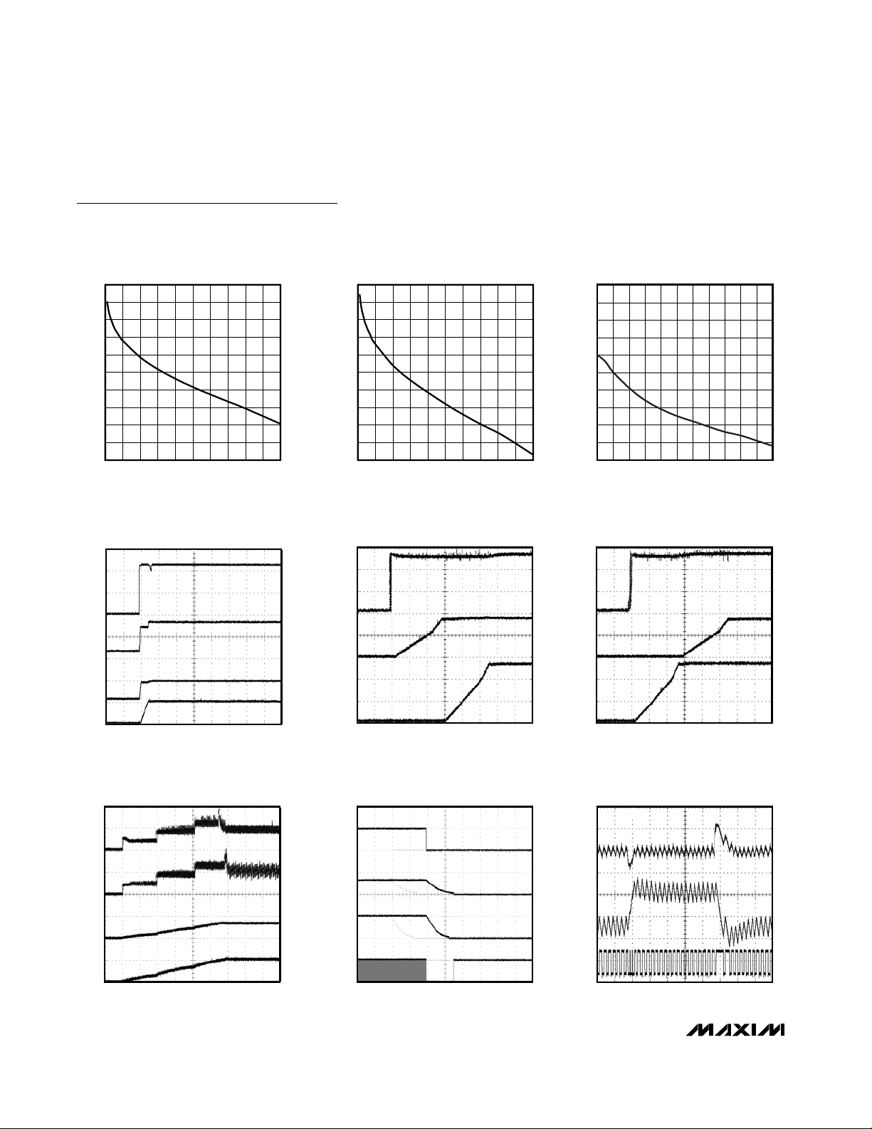
MAX1777/MAX1977/MAX1999
High-Efficiency, Quad Output, Main PowerSupply Controllers for Notebook Computers
10 ______________________________________________________________________________________
Typical Operating Characteristics (continued)
(Circuit of Figure 1 and Figure 2, no load on LDO5, LDO3, OUT3, OUT5, and REF, V+ = 12V, ON3 = ON5 = VCC, SHDN = V+,
R
CS
= 7mΩ, V
ILIM
_ = 0.5V, TA= +25°C, unless otherwise noted.)
4.95
4.96
4.97
4.98
4.99
5.00
020304010 50 60 70 9080 100
LDO5 REGULATOR OUTPUT VOLTAGE
vs. OUTPUT CURRENT
MAX1777 toc19
LDO5 OUTPUT CURRENT (mA)
LDO5 OUTPUT VOLTAGE (V)
3.330
3.334
3.332
3.338
3.336
3.342
3.340
3.344
3.348
3.346
3.350
020304010 50 60 70 9080 100
LDO3 REGULATOR OUTPUT VOLTAGE
vs. OUTPUT CURRENT
MAX1777 toc20
LDO3 OUTPUT CURRENT (mA)
LDO3 OUTPUT VOLTAGE (V)
1.995
1.997
1.996
2.000
1.999
1.998
2.001
2.002
2.004
2.003
2.005
-10 10 200 30405060708090100
REFERENCE VOLTAGE
vs. OUTPUT CURRENT
MAX1777 toc21
I
REF
(µA)
V
REF
(V)
0
2V
5V
0
3.3V
0
12V
REF, LDO3, AND LDO5 POWER-UP
MAX1777 toc22
4ms/div
V+
5V/div
LDO3
2V/div
LDO5
5V/div
REF
2V/div
0
0
5V
0
3.3V
0
5V
DELAYED START WAVEFORMS
(ON3 = REF)
MAX1777 toc23
200µs/div
ON5
2V/div
OUT3
2V/div
OUT5
2V/div
0
5V
0
3.3V
0
5V
DELAYED START WAVEFORMS
(ON5 = REF)
MAX1777 toc24
200µs/div
ON3
2V/div
OUT3
2V/div
OUT5
2V/div
0
5A
0
3.3V
0
5A
SOFT-START WAVEFORMS
MAX1777 toc25
200µs/div
I
L5
5A/div
OUT3
5V/div
OUT5
5V/div
I
L3
5A/div
0
5V
0
3.3V
0
5V
0
5V
SHUTDOWN WAVEFORMS
MAX1777 toc26
10ms/div
ON3
5V/div
OUT5
5V/div
DL3
5V/div
OUT3
5V/div
0
5V
SWITCHING
0
4A
1A
5V
MAX1777/MAX1999 (TON = VCC)
5V PWM-MODE
LOAD TRANSIENT RESPONSE
MAX1777 toc27
20µs/div
V
OUT
,
ACCOUPLED
100mV/div
INDUCTOR
CURRENT
2A/div
DL5
5V/div
5V
Page 11

MAX1777/MAX1977/MAX1999
High-Efficiency, Quad Output, Main Power-
Supply Controllers for Notebook Computers
______________________________________________________________________________________ 11
0
4A
1A
5V
MAX1977/MAX1999 (TON = GND)
5V PWM-MODE
LOAD TRANSIENT RESPONSE
MAX1777 toc28
10µs/div
V
OUT
,
ACCOUPLED
100mV/div
INDUCTOR
CURRENT
2A/div
DL5
5V/div
5V
0
4A
1A
3.3V
MAX1777/MAX1999 (TON = VCC)
3.3V PWM-MODE
LOAD TRANSIENT RESPONSE
MAX1777 toc29
20µs/div
V
OUT
,
ACCOUPLED
100mV/div
INDUCTOR
CURRENT
2A/div
DL3
5V/div
5V
0
4A
1A
3.3V
MAX1977/MAX1999 (TON = GND)
3.3V PWM-MODE
LOAD TRANSIENT RESPONSE
MAX1777 toc30
10µs/div
V
OUT
,
ACCOUPLED
100mV/div
INDUCTOR
CURRENT
2A/div
DL3
5V/div
5V
5V ULTRASONIC EFFICIENCY
vs. LOAD CURRENT (TON = V
CC
)
MAX1777 toc31
LOAD CURRENT (A)
EFFICIENCY (%)
10.10.01
10
20
30
40
50
60
70
80
90
100
0
0.001 10
VIN = 12V
VIN = 24V
5V ULTRASONIC EFFICIENCY
vs. LOAD CURRENT (TON = GND)
MAX1777 toc32
LOAD CURRENT (A)
EFFICIENCY (%)
10.10.01
10
20
30
40
50
60
70
80
90
100
0
0.001 10
VIN = 12V
VIN = 24V
3.3V ULTRASONIC EFFICIENCY
vs. LOAD CURRENT (TON = V
CC
)
MAX1777 toc33
LOAD CURRENT (A)
EFFICIENCY (%)
10.10.01
10
20
30
40
50
60
70
80
90
100
0
0.001 10
VIN = 7V
VIN = 12V
VIN = 24V
3.3V ULTRASONIC EFFICIENCY
vs. LOAD CURRENT (TON = GND)
MAX1777 toc34
LOAD CURRENT (A)
EFFICIENCY (%)
10.10.01
10
20
30
40
50
60
70
80
90
100
0
0.001 10
VIN = 7V
VIN = 12V
VIN = 24V
Typical Operating Characteristics (continued)
(Circuit of Figure 1 and Figure 2, no load on LDO5, LDO3, OUT3, OUT5, and REF, V+ = 12V, ON3 = ON5 = VCC, SHDN = V+,
R
CS
= 7mΩ, V
ILIM
_ = 0.5V, TA= +25°C, unless otherwise noted.)
Page 12

MAX1777/MAX1977/MAX1999
High-Efficiency, Quad Output, Main PowerSupply Controllers for Notebook Computers
12 ______________________________________________________________________________________
Pin Description
PIN
MAX1777
MAX1977
FUNCTION
1 — CS3
3.3V SMPS Current-Sense Input. Connect CS3 to a current-sensing resistor from the source of
the synchronous rectifier to GND. The voltage at ILIM3 determines the current-limit threshold
(see the Current-Limit (ILIM) Circuit section).
— 1 N.C. No Connection. Not internally connected.
22
Power-Good Output. PGOOD is an open-drain output that is pulled low if either output is
disabled or is more than 10% below its nominal value.
3 3 ON3
3.3V SMPS Enable Input. The 3.3V SMPS is enabled if ON3 is greater than the SMPS on level
and disabled if ON3 is less than the SMPS off level. If ON3 is connected to REF, the 3.3V
SMPS starts after the 5V SMPS reaches regulation (delay start). Drive ON3 below the clear
fault level to reset the fault latches.
4 4 ON5
5V SMPS Enable Input. The 5V SMPS is enabled if ON5 is greater than the SMPS on level and
disabled if ON5 is less than the SMPS off level. If ON5 is connected to REF, the 5V SMPS
starts after the 3.3V SMPS reaches regulation (delay start). Drive ON5 below the clear fault
level to reset the fault latches.
55
3.3V SMPS Current-Limit Adjustment. The GND-LX current-limit threshold defaults to 100mV if
ILIM3 is tied to V
CC
. In adjustable mode, the current-limit threshold is 1/10th the voltage seen
at ILIM3 over a 0.5V to 3V range. The logic threshold for switchover to the 100mV default value
is approximately V
CC
- 1V. Connect ILIM3 to REF for a fixed 200mV threshold.
66
Shutdown Control Input. The device enters its 6µA supply current shutdown mode if
V
SHDN
is less than the SHDN input falling edge trip level and does not restart until V
SHDN
is
greater than the SHDN input rising edge trip level. Connect SHDN to V+ for automatic startup.
SHDN can be connected to V+ through a resistive voltage-divider to implement a
programmable undervoltage lockout.
7 7 FB3
3.3V SMPS Feedback Input. Connect FB3 to GND for fixed 3.3V operation. Connect FB3 to a
resistive voltage-divider from OUT3 to GND to adjust the output from 2V to 5.5V.
8 8 REF
2V Reference Output. Bypass to GND with a 0.22µF (min) capacitor. REF can source up to
100µA for external loads. Loading REF degrades FB_ and output accuracy according to the
REF load-regulation error.
9 9 FB5
5V SMPS Feedback Input. Connect FB5 to GND for fixed 5V operation. Connect FB5 to a
resistive voltage-divider from OUT5 to GND to adjust the output from 2V to 5.5V.
10 10 PRO
Overvoltage and Undervoltage Fault Protection Enable/Disable. Connect PRO to V
CC
to
disable undervoltage and overvoltage protection. Connect PRO to GND to enable
undervoltage and overvoltage protection (see the Fault Protection section).
11 11
5V SMPS Current-Limit Adjustment. The GND-LX current-limit threshold defaults to 100mV if
ILIM5 is tied to V
CC
. In adjustable mode, the current-limit threshold is 1/10th the voltage seen
at ILIM5 over a 0.5V to 3V range. The logic threshold for switchover to the 100mV default value
is approximately V
CC
- 1V. Connect ILIM5 to REF for a fixed 200mV threshold.
12 12 SKIP
Low-Noise Mode Control. Connect SKIP to GND for normal idle-mode (pulse-skipping)
operation or to V
CC
for PWM mode (fixed frequency). Connect to REF or leave floating for
ultrasonic mode (pulse skipping, 25kHz minimum).
MAX1999
NAME
PGOOD
ILIM3
SHDN
ILIM5
Page 13

MAX1777/MAX1977/MAX1999
High-Efficiency, Quad Output, Main Power-
Supply Controllers for Notebook Computers
______________________________________________________________________________________ 13
Pin Description (continued)
PIN
MAX1777
MAX1977
FUNCTION
13 — CS5
5V SMPS Current-Sense Input. Connect CS5 to a current-sensing resistor from the source of
the synchronous rectifier to GND. The voltage at ILIM5 determines the current-limit threshold
(see the Current-Limit Circuit section).
—13TON
Frequency Select Input. Connect to V
CC
for 200kHz/300kHz operation and to GND for
400kHz/500kHz operation (5V/3.3V SMPS switching frequencies, respectively).
14 14
Boost Flying Capacitor Connection for 5V SMPS. Connect to an external capacitor and diode
according to the Typical Application Circuits (Figure 1 and Figure 2). See the MOSFET Gate
Drivers (DH_, DL_) section.
15 15 LX5
Inductor Connection for 5V SMPS. LX5 is the internal lower supply rail for the DH5 high-side
gate driver. LX5 is the current-sense input for the 5V SMPS (MAX1999 only).
16 16 DH5 High-Side MOSFET Floating Gate-Driver Output for 5V SMPS. DH5 swings from LX5 to BST5.
17 17 V
CC
Analog Supply Voltage Input for PWM Core. Connect VCC to the system supply voltage with a
series 50Ω resistor. Bypass to GND with a 1µF ceramic capacitor.
18 18
5V Linear-Regulator Output. LDO5 is the gate-driver supply for the external MOSFETs. LDO5
can provide a total of 100mA, including MOSFET gate-drive requirements and external loads.
The internal load depends on the choice of MOSFET and switching frequency (see the
Reference and Linear Regulators (REF, LDO5, and LDO3) section). If OUT5 is greater than the
LDO5 bootstrap switch threshold, the LDO5 regulator shuts down and the LDO5 pin connects
to OUT5 through a 1.4Ω switch. Bypass LDO5 with a minimum of 4.7µF. Use an additional 1µF
per 5mA of load.
19 19 DL5 5V SMPS Synchronous Rectifier Gate-Drive Output. DL5 swings between GND and LDO5.
20 20 V+
Power-Supply Input. V+ powers the LDO5/LDO3 linear regulators and is also used for the
Quick-PWM on-time one-shot circuits. Connect V+ to the battery input through a 4Ω resistor
and bypass with a 4.7µF capacitor.
21 21
5V SMPS Output Voltage-Sense Input. Connect to the 5V SMPS output. OUT5 is an input to the
Quick-PWM on-time one-shot circuit. It also serves as the 5V feedback input in fixed-voltage
mode. If OUT5 is greater than the LDO5 bootstrap-switch threshold, the LDO5 linear regulator
shuts down and LDO5 connects to OUT5 through a 1.4Ω switch.
22 22
3.3V SMPS Output Voltage-Sense Input. Connect to the 3.3V SMPS output. OUT3 is an input to
the Quick-PWM on-time one-shot circuit. It also serves as the 3V feedback input in fixedvoltage mode. If OUT3 is greater than the LDO3 bootstrap-switch threshold, the LDO3 linear
regulator shuts down and LDO3 connects to OUT3 through a 1.5Ω switch.
23 23 GND Analog and Power Ground
24 24 DL3 3.3V SMPS Synchronous-Rectifier Gate-Drive Output. DL3 swings between GND and LDO5.
25 25
3.3V Linear-Regulator Output. LDO3 can provide a total of 100mA to external loads. If OUT3 is
greater than the LDO3 bootstrap-switch threshold, the LDO3 regulator shuts down and the
LDO3 pin connects to OUT3 through a 1.5Ω switch. Bypass LDO3 with a minimum of 4.7µF.
Use an additional 1µF per 5mA of load.
26 26 DH3
27 27 LX3
Inductor Connection for 3.3V SMPS. LX3 is the current-sense input for the 3.3V SMPS
(MAX1999 only).
28 28
Boost Flying Capacitor Connection for 3.3V SMPS. Connect to an external capacitor and diode
according to the Typical Application Circuits (Figure 1 and Figure 2). See the MOSFET Gate
Drivers (DH_, DL_) section.
MAX1999
NAME
BST5
LDO5
OUT5
OUT3
LDO3
BST3
High-Side MOSFET Floating Gate-Driver Output for 3.3V SMPS. DH3 swings from LX3 to BST3.
Page 14

MAX1777/MAX1977/MAX1999
High-Efficiency, Quad Output, Main PowerSupply Controllers for Notebook Computers
14 ______________________________________________________________________________________
Typical Application Circuit
The typical application circuits (Figures 1 and 2) generate the 5V/5A and 3.3V/5A main supplies in a notebook
computer. The input supply range is 7V to 24V. Table 1
lists component suppliers.
Detailed Description
The MAX1777/MAX1977/MAX1999 dual-buck, BiCMOS,
switch-mode power-supply controllers generate logic
supply voltages for notebook computers. The
MAX1777/MAX1977/MAX1999 are designed primarily
for battery-powered applications where high-efficiency
and low-quiescent supply current are critical.
The MAX1777 is optimized for highest efficiency with a
5V/200kHz SMPS and a 3.3V/300kHz SMPS, while the
MAX1777/
MAX1977
VIN 7V TO 24V
10µF
4.7µF
1/2
D1
0.1µF
0.1µF
N1
FDS6612A
L5
5V
C5
D3
EP10QY03
N2
IRF7811AV
ON
OFF
V
CC
REF
0.22µF
4.7µF
3.3V ALWAYS ON
1MΩ
100kΩ
V
CC
50Ω
1µF
5V ALWAYS ON
4.7µF
10µF
1µF
10µF
1/2
D1
CMPSH-3A
0.1µF
N3
FDS6612A
L3
3.3V
C3
D2
EP10QY03
N4
IRF7811AV
LDO5 ILIM3 V
CC
V+
BST5
DH5
LX5
CS5
DL5
OUT5
FB5
PGOOD
FB3
OUT3
DL3
LX3
DH3
BST3
ILIM5
ON5
ON3
GND
SHDN
REF LDO3
PRO
SKIP
400kHz/500kHz
MAX1977
200kHz/300kHz
MAX1777
5V/3.3V SMPS
SWITCHING FREQUENCY
L3
L5
C3
C5
4.7µH
7.6µH
470µF
330µF
3.0µH
5.6µH
220µF
150µF
FREQUENCY-DEPENDENT COMPONENTS
4Ω
10Ω
RCS5
20mΩ
RCS3
20mΩ
10Ω
CS3
Figure 1. MAX1777/MAX1977 Typical Application Circuit
MANUFACTURER PHONE
FACTORY FAX
Central Semiconductor
516-435-1824
Dale-Vishay
402-563-6418
Fairchild
408-721-1635
International Rectifier
310-322-3332
NIEC (Nihon)
847-843-2798
Sanyo
619-661-1055
Sprague
603-224-1430
Sumida
847-956-0702
Taiyo Yuden
408-573-4159
TDK
847-390-4405
Table 1. Component Suppliers
516-435-1110
402-564-3131
408-721-2181
310-322-3331
805-843-7500
619-661-6835
603-224-1961
847-956-0666
408-573-4150
847-390-4461
Page 15

MAX1777/MAX1977/MAX1999
High-Efficiency, Quad Output, Main Power-
Supply Controllers for Notebook Computers
______________________________________________________________________________________ 15
*OPTIONAL CAPACITANCE BETWEEN
LX AND PGND (CLOSE TO THE IC) ONLY
REQUIRED FOR ULTRASONIC MODE
MAX1999
VIN 7V TO 24V
10µF
4.7µF
1/2
D1
0.1µF
0.1µF
N1
FDS6612A
L5
5V
C5
D3
EP10QY03
N2
IRF7811AV
ON
OFF
V
CC
REF
0.22µF
4.7µF
3.3V ALWAYS ON
1MΩ
100kΩ
V
CC
50Ω
1µF
5V ALWAYS ON
4.7µF
10µF
1µF
10µF
1/2
D1
CMPSH-3A
0.1µF
N3
FDS6612A
L3
3.3V
C3
D2
EP10QY03
N4
IRF7811AV
LDO5 ILIM3 V
CC
V+
BST5
DH5
LX5
DL5
OUT5
FB5
PGOOD
FB3
OUT3
DL3
TON
LX3
DH3
BST3
ILIM5
ON5
ON3
GND
SHDN
REF LDO3
PRO
SKIP
400kHz/500kHz
TON = GND
200kHz/300kHz
TON = V
CC
5V/3.3V SMPS
SWITCHING FREQUENCY
L3
L5
C3
C5
4.7µH
7.6µH
470µF
330µF
3.0µH
5.6µH
220µF
150µF
FREQUENCY-DEPENDENT COMPONENTS
4Ω
SEE
TABLE
10Ω
470pF*
10Ω
470pF*
Figure 2. MAX1999 Typical Application Circuit
Page 16

MAX1777/MAX1977/MAX1999
High-Efficiency, Quad Output, Main PowerSupply Controllers for Notebook Computers
16 ______________________________________________________________________________________
MAX1977 is optimized for “thin and light” applications with a
5V/400kHz SMPS and a 3.3V/500kHz SMPS. The MAX1999
provides a pin-selectable switching frequency, allowing
either 200kHz/300kHz or 400kHz/500kHz operation of the
5V/3.3V SMPSs, respectively.
Light-load efficiency is enhanced by automatic Idle
Mode™ operation, a variable-frequency pulse-skipping
mode that reduces transition and gate-charge losses.
Each step-down, power-switching circuit consists of two
N-channel MOSFETs, a rectifier, and an LC output filter.
The output voltage is the average AC voltage at the
switching node, which is regulated by changing the duty
cycle of the MOSFET switches. The gate-drive signal to
the N-channel high-side MOSFET must exceed the
battery voltage, and is provided by a flying-capacitor
boost circuit that uses a 100nF capacitor connected to
BST_.
MAX1777/
MAX1977/
MAX1999
LDO5
DL3
CS3
(MAX1777/
MAX1977)
ILIM3
FB3
OUT3
LDO3
ON3
ON5
SHDN
PRO
2.91V
3V
LINEAR
REG
POWER-ON SEQUENCE/
CLEAR FAULT LATCH
EN3
THERMAL
SHUTDOWN
5V
LINEAR
REG
2V
REFERENCE
3.3V
SMPS PWM
CONTROLLER
5V
SMPS PWM
CONTROLLER
4.56V
PGOOD3
PGOOD5
PGOOD
LDO5
BST5
DH5
LX5
EN5
DL5
CS5
(MAX1777/
MAX1977)
ILIM5
FB5
OUT5
LDO5
V
CC
REF
V+
GND
TON
(MAX1999 ONLY)
BST3
DH3
LX3
Figure 3. Detailed Functional Diagram
Idle Mode is a trademark of Maxim Integrated Products, Inc.
Page 17

MAX1777/MAX1977/MAX1999
High-Efficiency, Quad Output, Main Power-
Supply Controllers for Notebook Computers
______________________________________________________________________________________ 17
Each PWM controller consists of a Dual Mode feedback
network and multiplexer, a multi-input PWM comparator,
high-side and low-side gate drivers, and logic. The
MAX1777/MAX1977/MAX1999 contain fault-protection circuits that monitor the main PWM outputs for undervoltage
and overvoltage conditions. A power-on sequence block
controls the power-up timing of the main PWMs and monitors the outputs for undervoltage faults. The
MAX1777/MAX1977/MAX1999 include 5V and 3.3V linear
regulators. Bias generator blocks include the 5V (LDO5)
linear regulator, 2V precision reference, and automatic
bootstrap switchover circuit.
ON-TIME
COMPUTE
t
ON
t
OFF
TRIG
TRIG
ONE SHOT
ONE SHOT
Q
Q
Q
R
S
ERROR
AMPLIFIER
CURRENT
LIMIT
ZERO
CROSSING
Q
R
S
FAULT
LATCH
20ms
BLANKING
OUT
REF
ILIM_
CS_ (MAX1777/1977)
LX_ (MAX1999)
SKIP
OUT_
FB_
0.15V
PRO
0.9
✕
V
REF
1.1 ✕ V
REF
0.7✕V
REF
OV_FAULT
UV_FAULT
PGOOD
TO DL_ DRIVER
TO DH_ DRIVER
Σ
TON (MAX1999)
V+
Figure 4. PWM Controller (One Side Only)
Page 18

MAX1777/MAX1977/MAX1999
High-Efficiency, Quad Output, Main PowerSupply Controllers for Notebook Computers
18 ______________________________________________________________________________________
These internal blocks are not powered directly from the
battery. Instead, the 5V (LDO5) linear regulator steps
down the battery voltage to supply both internal circuitry and the gate drivers. The synchronous-switch gate
drivers are directly powered from LDO5, while the highside switch gate drivers are indirectly powered from
LDO5 through an external diode-capacitor boost circuit. An automatic bootstrap circuit turns off the 5V linear regulator and powers the device from OUT5 when
OUT5 is above 4.56V.
Free-Running, Constant On-Time PWM
Controller with Input Feed Forward
The Quick-PWM control architecture is a pseudo-fixedfrequency, constant on-time, current-mode type with
voltage feedforward. The Quick-PWM control architecture relies on the output ripple voltage to provide the
PWM ramp signal, thus the output filter capacitor’s ESR
acts as a current-feedback resistor. The high-side
switch on-time is determined by a one-shot whose period is inversely proportional to input voltage and directly
proportional to output voltage. Another one-shot sets a
minimum off-time (300ns typ). The on-time one-shot
triggers when the following conditions are met: the error
comparator is low, the synchronous rectifier current is
below the current-limit threshold, and the minimum offtime one-shot has timed out.
On-Time One-Shot (tON)
Each PWM core includes a one-shot that sets the highside switch on-time for each controller. Each fast, lowjitter, adjustable one-shot includes circuitry that varies
the on-time in response to battery and output voltage.
The high-side switch on-time is inversely proportional to
the battery voltage as measured by the V+ input, and
proportional to the output voltage. This algorithm results
in a nearly constant switching frequency despite the
lack of a fixed-frequency clock generator. The benefit
of a constant switching frequency is the frequency can
be selected to avoid noise-sensitive frequency regions:
tON= K (V
OUT
+ 0.075V) / V+
See Table 2 for approximate K-factors. The constant
0.075V is an approximation to account for the expected
drop across the synchronous-rectifier switch. Switching
frequency increases as a function of load current due
to the increasing drop across the synchronous rectifier,
which causes a faster inductor-current discharge ramp.
On-times translate only roughly to switching frequencies. The on-times guaranteed in the Electrical
Characteristics are influenced by switching delays in
the external high-side power MOSFET. Also, the deadtime effect increases the effective on-time, reducing the
switching frequency. It occurs only in PWM mode (SKIP
= VCC) and during dynamic output voltage transitions
when the inductor current reverses at light or negative
load currents. With reversed inductor current, the
inductor’s EMF causes LX to go high earlier than normal, extending the on-time by a period equal to the DHrising dead time.
For loads above the critical conduction point, the actual
switching frequency is:
where V
DROP1
is the sum of the parasitic voltage drops
in the inductor discharge path, including synchronous
rectifier, inductor, and PC board resistances; V
DROP2
is
the sum of the parasitic voltage drops in the charging
path, including high-side switch, inductor, and PC
board resistances, and t
ON
is the on-time calculated by
the MAX1777/MAX1977/MAX1999.
Automatic Pulse-Skipping Switchover
(Idle Mode)
In Idle Mode (SKIP = GND), an inherent automatic
switchover to PFM takes place at light loads. This
switchover is affected by a comparator that truncates
the low-side switch on-time at the inductor current’s
zero crossing. This mechanism causes the threshold
between pulse-skipping PFM and nonskipping PWM
operation to coincide with the boundary between con-
f
VV
tVV
OUT DROP
ON DROP
=
+
++
()
1
2
SMPS
SWITCHING
FREQUENCY (kHz)
K-FACTOR (µs)
APPROXIMATE K-
FACTOR ERROR (%)
MAX1777/MAX1999 (tON = VCC), 5V 200 5.0 ±10
MAX1777/MAX1999 (tON = VCC), 3.3V 300 3.3 ±10
MAX1977/MAX1999 (tON = GND), 5V 400 2.5 ±10
MAX1977/MAX1999 (tON = GND), 3.3V 500 2.0 ±10
Table 2. Approximate K-Factor Errors
Page 19

MAX1777/MAX1977/MAX1999
High-Efficiency, Quad Output, Main Power-
Supply Controllers for Notebook Computers
______________________________________________________________________________________ 19
tinuous and discontinuous inductor-current operation
(also known as the critical conduction point):
where K is the on-time scale factor (see the On-Time
One-Shot (tON) section). The load-current level at which
PFM/PWM crossover occurs, I
LOAD(SKIP)
, is equal to 1/2
the peak-to-peak ripple current, which is a function of the
inductor value (Figure 5). For example, in the MAX1777
typical application circuit with V
OUT2
= 5V, V+ = 12V,
L = 7.6µH, and K = 5µs, switchover to pulse-skipping
operation occurs at I
LOAD
= 0.96A or about 1/5 full load.
The crossover point occurs at an even lower value if a
swinging (soft-saturation) inductor is used.
The switching waveforms may appear noisy and asynchronous when light loading causes pulse-skipping
operation, but this is a normal operating condition that
results in high light-load efficiency. Trade-offs in PFM
noise vs. light-load efficiency are made by varying the
inductor value. Generally, low inductor values produce
a broader efficiency vs. load curve, while higher values
result in higher full-load efficiency (assuming that the
coil resistance remains fixed) and less output voltage
ripple. Penalties for using higher inductor values
include larger physical size and degraded load-transient response (especially at low input voltage levels).
DC output accuracy specifications refer to the trip level of
the error comparator. When the inductor is in continuous
conduction, the output voltage has a DC regulation higher than the trip level by 50% of the ripple. In discontinuous conduction (SKIP = GND, light load), the output
voltage has a DC regulation higher than the trip level by
approximately 1.5% due to slope compensation.
Forced-PWM Mode
The low-noise, forced-PWM (SKIP = VCC) mode disables the zero-crossing comparator, which controls the
low-side switch on-time. Disabling the zero-crossing
detector causes the low-side, gate-drive waveform to
become the complement of the high-side, gate-drive
waveform. The inductor current reverses at light loads
as the PWM loop strives to maintain a duty ratio of
V
OUT
/V+. The benefit of forced-PWM mode is to keep
the switching frequency fairly constant, but it comes at
a cost: the no-load battery current can be 10mA to
50mA, depending on switching frequency and the
external MOSFETs.
Forced-PWM mode is most useful for reducing audiofrequency noise, improving load-transient response,
providing sink-current capability for dynamic output
voltage adjustment, and improving the cross-regulation
of multiple-output applications that use a flyback transformer or coupled inductor.
Minimum 25kHz Pulse-Skipping Mode
(Ultrasonic Mode)
Leaving SKIP unconnected or connecting SKIP to REF
activates a pulse-skipping mode with a minimum
switching frequency of 25kHz. This ultrasonic pulseskipping mode reduces audio-frequency modulation of
the power supply that may occur in Idle Mode at very
light loads. The transition to fixed-frequency PWM operation is automatic and occurs at the same point as in
Idle Mode. Ultrasonic pulse skipping occurs if no
switching has taken place within the last 28µs. DL_
turns on to induce a regulated negative current in the
inductor. DH_ turns on when the inductor current
reaches the regulated negative current limit. Starting
with a DL_ pulse greatly reduces the ripple current
when compared to starting with a DH_ pulse (Idle
Mode). The output voltage level determines the negative current limit.
Calculate the negative ultrasonic current-limit threshold
with the following equation:
where VFB> V
REF
, and RONis the on-resistance of the
synchronous rectifier (MAX1999) or the current-sense
resistor value (MAX1777/MAX1977).
VIR
VV
V
V
NEG LX ON
REF FB
ILIM
SU
=× =
−
×
()
._0 467
I
KV
L
VV
V
LOAD SKIP
OUT OUT
()
__
=
×
×
+−
+
⎛
⎝
⎜
⎞
⎠
⎟
2
INDUCTOR CURRENT
I
LOAD
= I
PEAK
/2
ON-TIME0 TIME
-I
PEAK
L
V+
- V
OUT
∆
i
∆
t
=
Figure 5. Pulse- Skipping/Discontinuous Crossover Point
Page 20

MAX1777/MAX1977/MAX1999
High-Efficiency, Quad Output, Main PowerSupply Controllers for Notebook Computers
20 ______________________________________________________________________________________
Reference and Linear Regulators
(REF, LDO5, and LDO3)
The 2V reference (REF) is accurate to ±1% over temperature, making REF useful as a precision system reference. Bypass REF to GND with a 0.22µF minimum
capacitor. REF can supply up to 100µA for external
loads. However, if extremely accurate specifications for
both the main output voltages and REF are essential,
avoid loading REF. Loading REF reduces the LDO5,
LDO3, OUT5, and OUT3 output voltages slightly,
because of the reference load-regulation error.
Two internal regulators produce 5V (LDO5) and
3.3V(LDO3). LDO5 provides gate drive for the external
MOSFETs and powers the PWM controller, logic, reference, and other blocks within the device. The LDO5
regulator supplies a total of 100mA for internal and
external loads, including MOSFET gate drive, which
typically varies from 10mA to 50mA, depending on
switching frequency and the external MOSFETs. LDO3
supplies up to 100mA for external loads. Bypass LDO5
and LDO3 with a minimum of 4.7µF load, use an additional 1µF per 5mA of internal and external load.
When the 5V main output voltage is above the LDO5
bootstrap-switchover threshold, an internal 1.4Ω P-chan-
nel MOSFET switch connects OUT5 to LDO5, while simultaneously shutting down the LDO5 linear regulator.
Similarly, when the 3.3V main output voltage is above the
LDO3 bootstrap-switchover threshold, an internal 1.5Ω
P-channel MOSFET switch connects OUT3 to LDO3,
while simultaneously shutting down the LDO3 linear regulator. These actions bootstrap the device, powering the
internal circuitry and external loads from the output SMPS
voltages, rather than through linear regulators from the
battery. Bootstrapping reduces power dissipation due to
gate charge and quiescent losses by providing power
from a 90%-efficient switch-mode source, rather than
from a much-less-efficient linear regulator.
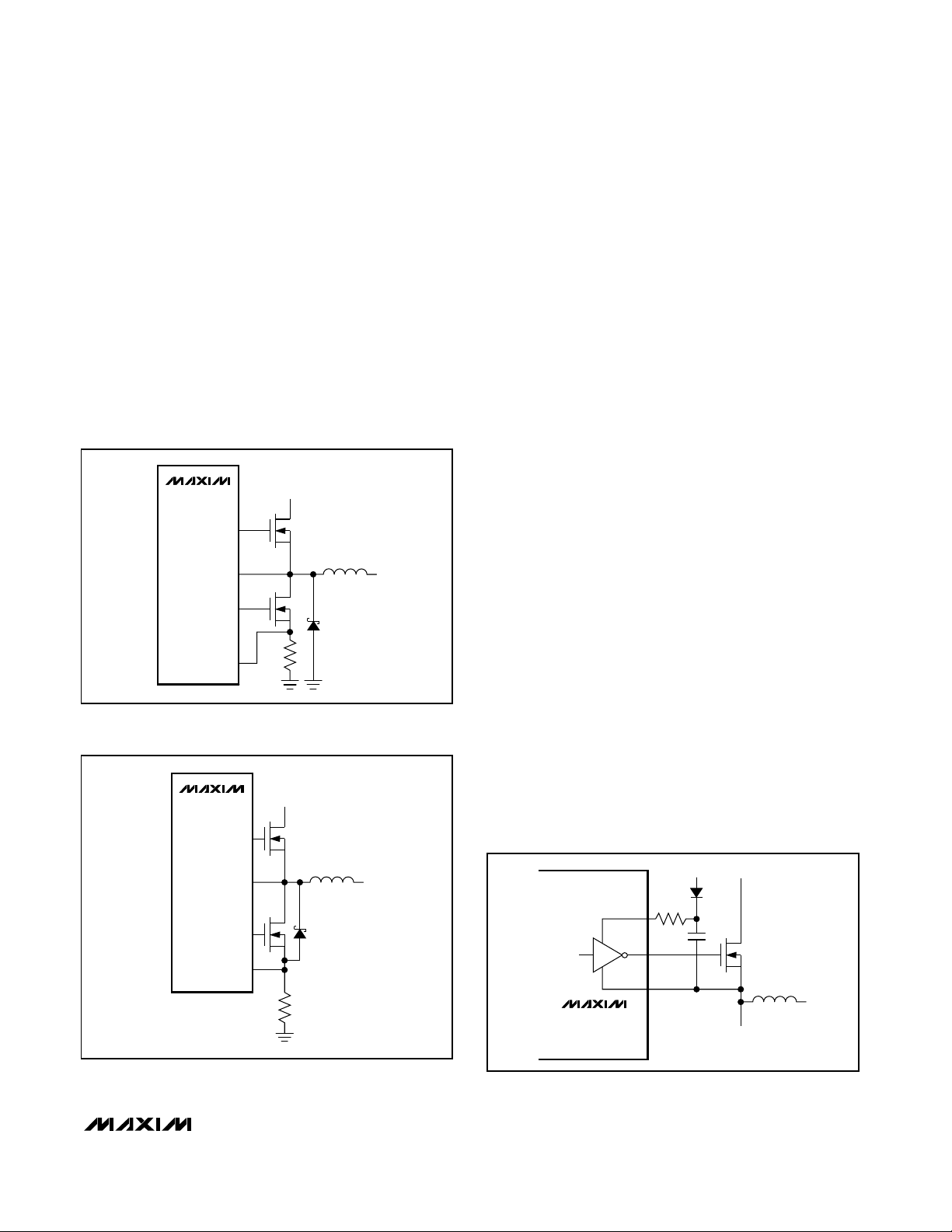
Current Limit Circuit (ILIM_)
The current-limit circuit employs a “valley” current-sensing algorithm. The MAX1999 uses the on-resistance of
the synchronous rectifier, while the MAX1777/MAX19777
uses a discrete resistor in series with the source of the
synchronous rectifier as a current-sensing element. If the
magnitude of the current-sense signal at CS_
(MAX1777/MAX1977) / LX_ (MAX1999) is above the current-limit threshold, the PWM is not allowed to initiate a
new cycle (Figure 6). The actual peak current is greater
than the current-limit threshold by an amount equal to the
inductor ripple current. Therefore, the exact current-limit
characteristic and maximum load capability are a function of the current-limit threshold, inductor value, and
input and output voltage.
For the MAX1777/MAX1977, connect CS_ to the junction
of the synchronous rectifier source and a current-sense
resistor to GND. With a current-limit threshold of 100mV,
the accuracy is approximately ±7%. Using a lower current-sense threshold results in less accuracy. The current-sense resistor only dissipates power when the
synchronous rectifier is on.
For lower power dissipation, the MAX1999 uses the onresistance of the synchronous rectifier as the currentsense element (Figure 7). Use the worst-case maximum
value for R
DS(ON)
from the MOSFET data sheet, and
add some margin for the rise in R
DS(ON)
with temperature. A good general rule is to allow 0.5% additional
resistance for each °C of temperature rise. The current
limit varies with the on-resistance of the synchronous
rectifier. The reward for this uncertainty is robust, lossless overcurrent sensing. When combined with the
undervoltage protection circuit, this current-limit
method is effective in almost every circumstance.
INDUCTOR CURRENT
I
LIMIT
I
LOAD
0 TIME
-I
PEAK
Figure 6. “Valley” Current-Limit Threshold Point
MAX1999
V+
DH_
DL_
LX_
OUT_
Figure 7. Current Sensing Using R
DS(ON)
of Synchronous
Rectifier
Page 21
MAX1777/MAX1977/MAX1999
High-Efficiency, Quad Output, Main Power-
Supply Controllers for Notebook Computers
______________________________________________________________________________________ 21
A negative current limit prevents excessive reverse
inductor currents when V
OUT
sinks current. The negative current-limit threshold is set to approximately 120%
of the positive current limit and therefore tracks the
positive current limit when ILIM_ is adjusted.
The current-limit threshold is adjusted with an external
voltage-divider at ILIM_. The current-limit threshold
adjustment range is from 50mV to 300mV. In the
adjustable mode, the current-limit threshold voltage is
precisely 1/10th the voltage at ILIM_. The threshold
defaults to 100mV when ILIM_ is connected to VCC.
The logic threshold for switchover to the 100mV default
value is approximately VCC- 1V.
Carefully observe the PC board layout guidelines to
ensure that noise and DC errors do not corrupt the current-sense signals at CS_. Mount or place the device
close to the synchronous rectifier or sense resistor
(whichever is used) with short, direct traces, making a
Kelvin sense connection to the sense resistor. The current-sense accuracy of Figure 8 is degraded if the
Schottky diode conducts during the synchronous rectifier on-time. To ensure that all current passes through
the sense resistor, connect the Schottky diode in parallel with only the synchronous recifier (Figure 9) if the
voltage drop across the synchronous rectifier and
sense resistor exceeds the Schottky diode’s forward
voltage. Note that at high temperatures, the on-resistance of the synchronous rectifier increases, and the
forward voltage of the Schottky diode decreases.
MOSFET Gate Drivers (DH_, DL_)
The DH_ and DL_ gate drivers sink 2.0A and 3.3A
respectively of gate drive, ensuring robust gate drive for
high-current applications. The DH_ floating high-side
MOSFET drivers are powered by diode-capacitor charge
pumps at BST_. The DL_ synchronous-rectifier drivers are
powered by LDO5.
The internal pulldown transistors that drive DL_ low
have a 0.6Ω typical on-resistance. These low on-resis-
tance pulldown transistors prevent DL_ from being
pulled up during the fast rise time of the inductor nodes
due to capacitive coupling from the drain to the gate of
the low-side synchronous-rectifier MOSFETs. However,
for high-current applications, some combinations of
high- and low-side MOSFETS may cause excessive
gate-drain coupling, which leads to poor efficiency and
EMI-producing shoot-through currents. Adding a resistor in series with BST_ increases the turn-on time of the
high-side MOSFETs at the expense of efficiency, without
degrading the turn-off time (Figure 10).
MAX1777
MAX1977
V+
DH_
DL_
CS_
LX_
OUT_
Figure 8. Current Sensing Using Sense Resistor
(MAX1777/MAX1977)
MAX1777
MAX1977
V+
DH_
DL_
CS_
LX_
OUT_
Figure 9. More Accurate Current Sensing with Adjusted
Schottky Connection
MAX1777
MAX1977
MAX1999
5V
V
IN
10Ω
BST
DH
LX
Figure 10. Reducing the Switching-Node Rise Time
Page 22

MAX1777/MAX1977/MAX1999
High-Efficiency, Quad Output, Main PowerSupply Controllers for Notebook Computers
22 ______________________________________________________________________________________
Adaptive dead-time circuits monitor the DL_ and DH_
drivers and prevent either FET from turning on until the
other is fully off. This algorithm allows operation without
shoot-through with a wide range of MOSFETs, minimizing delays and maintaining efficiency. There must be
low-resistance, low-inductance paths from the gate drivers to the MOSFET gates for the adaptive dead-time circuit to work properly. Otherwise, the sense circuitry
interprets the MOSFET gate as “off” when there is actually charge left on the gate. Use very short, wide traces
measuring 10 to 20 squares (50mils to 100mils wide if
the MOSFET is 1in from the device).
POR, UVLO, and Internal Digital
Soft-Start
Power-on reset (POR) occurs when V+ rises above
approximately 1V, resetting the undervoltage, overvoltage, and thermal-shutdown fault latches. LDO5
undervoltage lockout (UVLO) circuitry inhibits switching
when LDO5 is below 4V. DL_ is low if PRO is disabled;
DL_ is high if PRO is enabled. The output voltages
begin to ramp up as LDO5 rises above 4V. The internal
digital soft-start timer begins to ramp up the maximum
allowed current limit during startup. The 1.7ms ramp
occurs in five steps: 20%, 40%, 60%, 80%, and 100%.
Power-Good Output (PGOOD)
The PGOOD comparator continuously monitors both output voltages for undervoltage conditions. PGOOD is
actively held low in shutdown, standby, and soft-start.
PGOOD releases and digital soft-start terminates when
both outputs reach the error-comparator threshold.
PGOOD goes low if either output turns off or is 10%
below its nominal regulation point. PGOOD is a true
open-drain output. Note that PGOOD is independent of
the state of PRO.
Fault Protection
The MAX1777/MAX1977/MAX1999 provide over/undervoltage fault protection. Drive PRO low to activate fault
protection. Drive PRO high to disable fault protection.
Once activated, the devices continuously monitor for
both undervoltage and overvoltage conditions.
Overvoltage Protection
When the output voltage is 11% above the set voltage,
the overvoltage fault protection activates. The synchronous rectifier turns on 100% and the high-side MOSFET
turns off. This rapidly discharges the output capacitors,
decreasing the output voltage. The output voltage may
dip below ground. For loads that cannot tolerate a negative voltage, place a power Schottky diode across the
output to act as a reverse-polarity clamp. In practical
applications, there is a fuse between the power source
(battery) and the external high-side switches. If the
overvoltage condition is caused by a short in the highside switch, turning the synchronous rectifier on 100%
creates an electrical short between the battery and
GND, blowing the fuse and disconnecting the battery
from the output. Once an overvoltage fault condition is
set, it can only be reset by toggling SHDN, ON_, or
cycling V+ (POR).
Undervoltage Protection
When the output voltage is 30% below the set voltage
for over 22ms (undervoltage shutdown blanking time),
the undervoltage fault protection activates. Both SMPSs
stop switching. The two outputs start to discharge (see
the Discharge Mode (Soft-Stop) section). When the out-
put voltage drops to 0.3V, the synchronous rectifiers
turn on, clamping the outputs to GND. Toggle SHDN,
ON_, or cycle V+ (POR) to clear the undervoltage fault
latch.
Thermal Protection
The MAX1777/MAX1977/MAX1999 have thermal shutdown to protect the devices from overheating. Thermal
shutdown occurs when the die temperature exceeds
+160°C. All internal circuitry shuts down during thermal
shutdown. The MAX1777/MAX1977/MAX1999 may trigger thermal shutdown if LDO_ is not bootstrapped from
OUT_ while applying a high input voltage on V+ and
drawing the maximum current (including short circuit)
from LDO_. Even if LDO_ is bootstrapped from OUT_,
overloading the LDO_ causes large power dissipation
on the bootstrap switches, which may result in thermal
shutdown. Cycling SHDN, ON3, or ON5, or a V+ (POR)
ends the thermal shutdown state.
Discharge Mode (Soft-Stop)
When PRO is low, and a transition to standby or shutdown mode occurs, or the output undervoltage fault
latch is set, the outputs discharge to GND through an
internal 12Ω switch, until the output voltages decrease
to 0.3V. The reference remains active to provide an
accurate threshold and to provide overvoltage protection. When both SMPS outputs discharge to 0.3V, the
DL_ synchronous rectifier drivers are forced high. The
synchronous rectifier drivers clamp the SMPS outputs
to GND. When PRO is high, the SMPS outputs do not
discharge, and the DL_ synchronous rectifier drivers
remain low.
Shutdown Mode
Drive SHDN below the precise SHDN input falling-edge
trip level to place the MAX1777/MAX1977/MAX1999 in
its low-power shutdown state. The MAX1777/MAX1977/
MAX1999 consume only 6µA of quiescent current while
Page 23

MAX1777/MAX1977/MAX1999
High-Efficiency, Quad Output, Main Power-
Supply Controllers for Notebook Computers
______________________________________________________________________________________ 23
in shutdown mode. When shutdown mode activates, the
reference turns off, making the threshold to exit shutdown inaccurate. To guarantee startup, drive SHDN
above 2V (SHDN input rising-edge trip level). For automatic shutdown and startup, connect SHDN to V+. If
PRO is low, both SMPS outputs are discharged to 0.3V
through a 12Ω switch before entering true shutdown.
The accurate 1V falling-edge threshold on SHDN can be
used to detect a specific analog voltage level and shut
the device down. Once in shutdown, the 1.6V risingedge threshold activates, providing sufficient hysteresis
for most applications. For additional hysteresis, the
undervoltage threshold can be made dependent on
REF or LDO_, which go to 0V in shutdown.
Power-Up Sequencing and
On/Off Controls (ON3, ON5)
ON3 and ON5 control SMPS power-up sequencing.
ON3 or ON5 rising above 2.4V enables the respective
outputs. ON3 or ON5 falling below 1.6V disables the
respective outputs.
Connecting ON3 or ON5 to REF forces the respective
outputs off while the other output is below regulation and
starts after that output regulates. The second SMPS
remains on until the first SMPS turns off, the device shuts
down, a fault occurs, or LDO5 goes into undervoltage
lockout. Both supplies begin their power-down sequence
immediately when the first supply turns off. Driving ON_
MODE CONDITION COMMENT
Power-Up LDO5 < UVLO threshold
Transitions to discharge mode after a V+ POR and after REF becomes valid.
LDO5, LDO3, REF remain active. DL_ is active if PRO is low.
Run
SHDN = high, ON3 or ON5
enabled
Normal operation
Overvoltage
Protection
Either output > 111% of
nominal level, PRO = low
DL_ is forced high. LDO3, LDO5 active. Exited by a V+ POR or by toggling
SHDN, ON3, or ON5.
Undervoltage
Protection
Either output < 70% of
nominal after 22ms timeout expires and output is
enabled, PRO = low
If PRO is low, DL_ is forced high after discharge mode terminates. LDO3,
LDO5 active. Exited by a V+ POR or by toggling SHDN, ON3, or ON5.
Discharge
PRO is low and either
SMPS output is still high in
either standby mode or
shutdown mode
Discharge switch (12Ω) connects OUT_ to PGND. One output may still run
while the other is in discharge mode. Activates when LDO_ is in UVLO, or
transition to UVLO, standby, or shutdown has begun. LDO3, LDO5 active.
Standby
ON5, ON3 < startup
threshold, SHDN = high
DL_ stays high if PRO is low. LDO3, LDO5 active.
Shutdown SHDN = low All circuitry off
Thermal Shutdown
TJ > +160°C All circuitry off. Exited by V+ POR or cycling SHDN, ON3, or ON5.
Table 3. Operating Mode Truth Table
SHDN (V) V
ON3
(V) V
ON5
(V) LDO5 LDO3 5V SMPS 3V SMPS
< 1.0 X X Off Off Off Off
> 2.4 < 1.6 < 1.6 On On Off Off
> 2.4 > 2.4 > 2.4 On On On On
> 2.4 > 2.4 < 1.6 On On Off On
> 2.4 < 1.6 > 2.4 On On On Off
> 2.4 > 2.4 REF On On
On (after 3V
SMPS is up)
On
> 2.4 REF > 2.4 On On On
On (after 5V
SMPS is up)
Table 4. Power-Up Sequencing
Page 24

MAX1777/MAX1977/MAX1999
High-Efficiency, Quad Output, Main PowerSupply Controllers for Notebook Computers
24 ______________________________________________________________________________________
below 0.8V clears the overvoltage, undervoltage, and
thermal fault latches.
Adjustable-Output Feedback
(Dual-Mode FB)
Connect FB_ to GND to enable the fixed, preset SMPS
output voltages (3.3V and 5V). Connect a resistive voltage-divider at FB_ between OUT_ and GND to adjust
the respective output voltage between 2V and 5.5V
(Figure 11). Choose R2 to be about 10kΩ and solve for
R1 using the equation:
where V
FB
= 2V nominal.
When using the adjustable output mode, set the 3.3V
SMPS lower than the 5V SMPS. LDO5 connects to OUT5
through an internal switch only when OUT5 is above the
LDO5 bootstrap-switch threshold (4.56V). LDO3 connects to OUT3 through an internal switch only when
OUT3 is above the LDO3 bootstrap switch threshold
(2.91V). Bootstrapping is most effective when the fixed
output voltages are used. Once LDO_ is bootstrapped
from OUT_, the internal linear regulator turns off. This
reduces internal power dissipation and improves efficiency when LDO_ is powered with a high input voltage.
Design Procedure
Establish the input voltage range and maximum load
current before choosing an inductor and its associated
ripple-current ratio (LIR). The following four factors dictate the rest of the design:
1) Input Voltage Range. The maximum value (V+
(MAX)
)
must accommodate the maximum AC adapter voltage. The minimum value (V+
(MIN)
) must account for
the lowest input voltage after drops due to connectors, fuses, and battery selector switches. Lower input
voltages result in better efficiency.
2) Maximum Load Current. The peak load current
(I
LOAD(MAX)
) determines the instantaneous component stress and filtering requirements, and thus drives output capacitor selection, inductor saturation
rating, and the design of the current-limit circuit.
The continuous load current (I
LOAD
) determines the
thermal stress and drives the selection of input
capacitors, MOSFETs, and other critical heat-contributing components.
3) Switching Frequency. This choice determines the
basic trade-off between size and efficiency. The
optimal frequency is largely a function of maximum
input voltage and MOSFET switching losses. The
MAX1777 has a nominal switching frequency of
200kHz for the 5V SMPS and 300kHz for the 3.3V
SMPS. The MAX1977 has a nominal switching frequency of 400kHz for the 5V SMPS and 500kHz for
the 3.3V SMPS. The MAX1999 has pin-selectable
switching frequency.
4) Inductor Ripple Current Ratio (LIR). LIR is the
ratio of the peak-peak ripple current to the average
inductor current. Size and efficiency trade-offs must
be considered when setting the inductor ripple current ratio. Low inductor values cause large ripple
currents, resulting in the smallest size, but poor efficiency and high output noise. The minimum practical inductor value is one that causes the circuit to
operate at critical conduction (where the inductor
current just touches zero with every cycle at maximum load). Inductor values lower than this grant no
further size reduction benefit.
The MAX1777/MAX1977/MAX1999s’ pulse-skipping
algorithm (SKIP = GND) initiates skip mode at the
critical conduction point. So the inductor’s operating point also determines the load current at which
PWM/PFM switchover occurs. The optimum point is
usually found between 20% and 50% ripple current.
RR
V
V
OUT
FB
12 1=× −
⎛
⎝
⎜
⎜
⎞
⎠
⎟
⎟
_
MAX1777
MAX1977
MAX1999
DH_
DL_
GND
OUT_
FB_
V+
R1
R2
V
OUT_
Figure 11. Setting V
OUT_
with a Resistor-Divider
Page 25

MAX1777/MAX1977/MAX1999
High-Efficiency, Quad Output, Main Power-
Supply Controllers for Notebook Computers
______________________________________________________________________________________ 25
Inductor Selection
The switching frequency (on-time) and operating point
(% ripple or LIR) determine the inductor value as follows:
Example: I
LOAD(MAX)
= 5A, V+ = 12V, V
OUT5
= 5V, f =
200kHz, 35% ripple current or LIR = 0.35:
Find a low-loss inductor having the lowest possible DC
resistance that fits in the allotted dimensions. Ferrite cores
are often the best choice. The core must be large enough
not to saturate at the peak inductor current (I
PEAK
):
I
PEAK
= I
LOAD(MAX)
+ [(LIR/2) x I
LOAD(MAX)
]
The inductor ripple current also impacts transientresponse performance, especially at low V+ - V
OUT_
difference. Low inductor values allow the inductor current to slew faster, replenishing charge removed from
the output filter capacitors by a sudden load step. The
peak amplitude of the output transient (V
SAG
) is also a
function of the maximum duty factor, which can be calculated from the on-time and minimum off-time:
where minimum off-time = 0.350µs (max) and K is from
Table 2.
Determining the Current Limit
The minimum current-limit threshold must be great
enough to support the maximum load current when the
current limit is at the minimum tolerance value. The valley of the inductor current occurs at I
LOAD(MAX)
minus
half of the ripple current; therefore,
I
LIMIT(LOW)
> I
LOAD(MAX)
- [(LIR / 2) x I
LOAD(MAX)
]
where I
LIMIT(LOW)
= minimum current-limit threshold
voltage divided by the R
DS(ON)
of N2/N4 (MAX1999).
For the MAX1777/MAX1977/MAX1999, the minimum
current-limit threshold voltage is 93mV (ILIM_ = VCC).
Use the worst-case maximum value for R
DS(ON)
from
the MOSFET N2/N4 data sheet and add some margin
for the rise in R
DS(ON)
with temperature. A good gener-
al rule is to allow 0.5% additional resistance for each °C
of temperature rise.
Examining the 5A circuit example with a maximum
R
DS(ON)
= 12mΩ at high temperature reveals the following:
I
LIMIT(LOW)
= 93mV / 12mΩ > 5A - (0.35 / 2) 5A
7.75A > 4.125A
7.75A is greater than the valley current of 4.125A, so
the circuit can easily deliver the full-rated 5A using the
fixed 100mV nominal current-limit threshold voltage.
Connect the source of the synchronous rectifier to a
current-sense resistor to GND (MAX1777/MAX1977),
and connect CS_ to that junction to set the current limit
for the device. The MAX1777/MAX1977/MAX1999 limit
the current with the sense resistor instead of the
R
DS(ON)
of N2/N4. The maximum value of the sense
resistor can be calculated with the equation
I
LIM_
= 93mV / R
SENSE
Output Capacitor Selection
The output filter capacitor must have low enough equivalent series resistance (ESR) to meet output ripple and
load-transient requirements, yet have high enough ESR
to satisfy stability requirements. The output capacitance must also be high enough to absorb the inductor
energy while transitioning from full-load to no-load conditions without tripping the overvoltage fault latch. In
applications where the output is subject to large load
transients, the output capacitor’s size depends on how
much ESR is needed to prevent the output from dipping too low under a load transient. Ignoring the sag
due to finite capacitance:
where V
DIP
is the maximum tolerable transient voltage
drop. In non-CPU applications, the output capacitor’s
size depends on how much ESR is needed to maintain
an acceptable level of output voltage ripple:
where V
P-P
is the peak-to-peak output voltage ripple.
The actual capacitance value required relates to the
physical size needed to achieve low ESR, as well as to
the chemistry of the capacitor technology. Thus, the
capacitor is usually selected by ESR and voltage rating
rather than by capacitance value (this is true of tantalum, OS-CON, and other electrolytic-type capacitors).
R
V
LIR I
ESR
PP
LOAD MAX
≤
×
−
()
R
V
I
ESR
DIP
LOAD MAX
≤
()
V
ILK
V
V
t
CVK
VV
V
t
SAG
LOAD MAX
OUT
OFF MIN
OUT OUT
OUT
OFF MIN
=
∆
()
×
+
+
⎛
⎝
⎜
⎜
⎞
⎠
⎟
⎟
××
+−
+
⎛
⎝
⎜
⎜
⎞
⎠
⎟
⎟
−
⎡
⎣
⎢
⎢
⎤
⎦
()
_
()
_
_
()
2
2
L
VVV
V kHz A
H=
−
()
×××
=
512 5
12 200 0 35 5
83
.
. µ
L
VVV
V f LIR I
OUT OUT
LOAD MAX
=
+−
()
+× × ×
__
()
Page 26

MAX1777/MAX1977/MAX1999
High-Efficiency, Quad Output, Main PowerSupply Controllers for Notebook Computers
26 ______________________________________________________________________________________
When using low-capacity filter capacitors such as
polymer types, capacitor size is usually determined by
the capacity required to prevent V
SAG
and V
SOAR
from
tripping the undervoltage and overvoltage fault latches
during load transients in ultrasonic mode .
For low input-to-output voltage differentials (V
IN/VOUT
<2),
additional output capacitance is required to maintain stability and good efficiency in ultrasonic mode.
The amount of overshoot due to stored inductor energy
can be calculated as:
where I
PEAK
is the peak inductor current.
Stability Considerations
Stability is determined by the value of the ESR zero
(f
ESR
) relative to the switching frequency (f). The point
of instability is given by the following equation:
where:
For a typical 300kHz application, the ESR zero frequency must be well below 95kHz, preferably below 50kHz.
Low-ESR capacitors (especially polymer or tantalum),
in widespread use at the time of publication, typically
have ESR zero frequencies lower than of 30kHz. In the
design example used for inductor selection, the ESR
needed to support a specified ripple voltage is found
by the equation:
where LIR is the inductor ripple current ratio and I
LOAD
is the average DC load. Using a LIR = 0.35 and an
average load current of 5A, the ESR needed to support
50mV
P-P
ripple is 28mΩ.
Do not place high-value ceramic capacitors directly
across the fast-feedback inputs (OUT_ to GND for internal feedback, FB_ divider point for external feedback)
without taking precautions to ensure stability. Large
ceramic capacitors can have a high-ESR zero frequency
and cause erratic, unstable operation. Adding a discrete
resistor or placing the capacitors a couple of inches
downstream from the junction of the inductor and OUT_
may improve stability.
Unstable operation manifests itself in two related but
distinctly different ways: double pulsing and fast-feedback loop instability. Noise on the output or insufficient
ESR may cause double pulsing. Insufficient ESR does
not allow the amplitude of the voltage ramp in the output
signal to be large enough. The error comparator mistakenly triggers a new cycle immediately after the 350ns
minimum off-time period has expired. Double pulsing
results in increased output ripple, and can indicate the
presence of loop instability caused by insufficient ESR.
Loop instability results in oscillations or ringing at the
output after line or load perturbations, causing the output voltage to fall below the tolerance limit.
The easiest method for checking stability is to apply a
very fast zero-to-max load transient (refer to the
MAX1999 EV kit data sheet) and observe the output
voltage-ripple envelope for overshoot and ringing.
Monitoring the inductor current with an AC current
probe may also provide some insight. Do not allow
more than one cycle of ringing of under- or overshoot
after the initial step response.
Input Capacitor Selection
The input capacitors must meet the input ripple current
(I
RMS
) requirement imposed by the switching current.
The MAX1777/MAX1977/MAX1999 dual switching regulators operate at different frequencies. This interleaves
the current pulses drawn by the two switches and
reduces the overlap time where they add together. The
input RMS current is much smaller in comparison than
with both SMPSs operating in phase. The input RMS current varies with load and the input voltage.
The maximum input capacitor RMS current for a single
SMPS is given by:
when V+ = 2 x V
OUT_
(D = 50%), I
RMS
has maximum
current of I
LOAD
/2.
The ESR of the input capacitor is important for determining capacitor power dissipation. All the power
(I
2
RMS
x ESR) heats up the capacitor and reduces efficiency. Nontantalum chemistries (ceramic or OS-CON)
are preferred due to their low ESR and resilience to
power-up surge currents. Choose input capacitors that
exhibit less than +10°C temperature rise at the RMS
input current for optimal circuit longevity. Place the
drains of the high-side switches close to each other to
share common input bypass capacitors.
II
VVV
V
RMS LOAD
OUT OUT
≈
+−
()
+
⎛
⎝
⎜
⎜
⎜
⎞
⎠
⎟
⎟
⎟
__
ESR
V
LIR I
RIPPLE P P
LOAD
()
=
×
−
f
RC
ESR
ESR OUT
=
×× ×
1
2 π
f
f
ESR
≤
π
V
LI
CV
SOAR
PEAK
OUT
=
×
××
_
2
2
Page 27

MAX1777/MAX1977/MAX1999
High-Efficiency, Quad Output, Main Power-
Supply Controllers for Notebook Computers
______________________________________________________________________________________ 27
Power MOSFET Selection
Most of the following MOSFET guidelines focus on the
challenge of obtaining high load-current capability
(>5A) when using high-voltage (>20V) AC adapters.
Low-current applications usually require less attention.
Choose a high-side MOSFET (N1/N3) that has conduction losses equal to the switching losses at the typical
battery voltage for maximum efficiency. Ensure that the
conduction losses at the minimum input voltage do not
exceed the package thermal limits or violate the overall
thermal budget. Ensure that conduction losses plus
switching losses at the maximum input voltage do not
exceed the package ratings or violate the overall thermal budget.
Choose a synchronous rectifier (N2/N4) with the lowest
possible R
DS(ON)
. Ensure the gate is not pulled up by the
high-side switch turning on due to parasitic drain-to-gate
capacitance, causing cross-conduction problems.
Switching losses are not an issue for the synchronous
rectifier in the buck topology, since it is a zero-voltage
switched device when using the buck topology.
MOSFET Power Dissipation
Worst-case conduction losses occur at the duty factor
extremes. For the high-side MOSFET, the worst-case
power dissipation (PD) due to the MOSFET’s R
DS(ON)
occurs at minimum battery voltage:
Generally, a small high-side MOSFET reduces switching losses at high input voltage. However, the R
DS(ON)
required to stay within package power-dissipation limits
often limits how small the MOSFET can be. The optimum situation occurs when the switching (AC) losses
equal the conduction (R
DS(ON)
) losses.
Switching losses in the high-side MOSFET can become
an insidious heat problem when maximum battery voltage is applied, due to the squared term in the CV
2
✕ f
switching loss equation. Reconsider the high-side
MOSFET chosen for adequate R
DS(ON)
at low battery
voltages if it becomes extraordinarily hot when subjected to V+
(MAX)
.
Calculating the power dissipation in N1/N3 due to
switching losses is difficult since it must allow for quantifying factors that influence the turn-on and turn-off
times. These factors include the internal gate resistance, gate charge, threshold voltage, source induc-
tance, and PC board layout characteristics. The following switching loss calculation provides only a very
rough estimate and is no substitute for bench evaluation, preferably including verification using a thermocouple mounted on N1/N3:
where C
RSS
is the reverse transfer capacitance of
N1/N3 and I
GATE
is the peak gate-drive source/sink
current.
For the synchronous rectifier, the worst-case power dis-
sipation always occurs at maximum battery voltage:
The absolute worst case for MOSFET power dissipation
occurs under heavy overloads that are greater than
I
LOAD(MAX)
but are not quite high enough to exceed
the current limit and cause the fault latch to trip. To
protect against this possibility, “overdesign” the circuit
to tolerate:
I
LOAD
= I
LIMIT(HIGH)
+ (LIR / 2 ) x I
LOAD(MAX)
where I
LIMIT(HIGH)
is the maximum valley current
allowed by the current-limit circuit, including threshold
tolerance and resistance variation.
Rectifier Selection
Current circulates from ground to the junction of both
MOSFETs and the inductor when the high-side switch is
off. As a consequence, the polarity of the switching
node is negative with respect to ground. This voltage is
approximately -0.7V (a diode drop) at both transition
edges while both switches are off (dead time). The drop
is I
L
x R
DS(ON)
when the low-side switch conducts.
The rectifier is a clamp across the synchronous rectifier
that catches the negative inductor swing during the dead
time between turning the high-side MOSFET off and the
synchronous rectifier on. The MOSFETs incorporate a
high-speed silicon body diode as an adequate clamp
diode if efficiency is not of primary importance. Place a
Schottky diode in parallel with the body diode to reduce
the forward voltage drop and prevent the N2/N4 MOSFET
body diodes from turning on during the dead time.
Typically, the external diode improves the efficiency by
1% to 2%. Use a Schottky diode with a DC current rating
equal to one-third of the load current. For example, use
PD N N
V
V
IR
OUT
MAX
LOAD DS
24 1
2
/
_
()
()
=−
+
⎛
⎝
⎜
⎞
⎠
⎟
××
PD N N switching
CV fI
I
RSS MAX LOAD
GATE
13
2
/
()
()
=
×+ ××
⎛
⎝
⎜
⎜
⎜
⎞
⎠
⎟
⎟
⎟
PD N N resis ce
V
V
IR
OUT
MIN
LOAD DS ON
( / tan )
_
()
()
13
2
=
+
⎛
⎝
⎜
⎞
⎠
⎟
×
×
Page 28

MAX1777/MAX1977/MAX1999
High-Efficiency, Quad Output, Main PowerSupply Controllers for Notebook Computers
28 ______________________________________________________________________________________
an MBR0530 (500mA-rated) type for loads up to 1.5A, a
1N5819 type for loads up to 3A, or a 1N5822 type for
loads up to 10A. The rectifier’s rated reverse breakdown
voltage must be at least equal to the maximum input voltage, preferably with a 20% derating factor.
Boost Supply Diode
A signal diode, such as a 1N4148, works well in most
applications. Use a small (20mA) Schottky diode for
slightly improved efficiency and dropout characteristics, if the input voltage can go below 6V. Do not use
large power diodes, such as 1N5817 or 1N4001, since
high-junction capacitance can force LDO5 to excessive
voltages.
Applications Information
Dropout Performance
The output voltage-adjust range for continuous-conduction operation is restricted by the nonadjustable 350ns
(max) minimum off-time one-shot. Use the slower 5V
SMPS for the higher of the two output voltages for best
dropout performance in adjustable feedback mode. The
duty-factor limit must be calculated using worst-case values for on- and off-times, when working with low input
voltages. Manufacturing tolerances and internal propagation delays introduce an error to the tONK factor. Also,
keep in mind that transient response performance of
buck regulators operated close to dropout is poor, and
bulk output capacitance must often be added (see the
V
SAG
equation in the Output Capacitor Selection section).
The absolute point of dropout occurs when the inductor
current ramps down during the minimum off-time
(∆I
DOWN
) as much as it ramps up during the on-time
(∆IUP). The ratio h = ∆IUP/∆I
DOWN
indicates the ability to
slew the inductor current higher in response to
increased load, and must always be greater than 1. As
h approaches 1, the absolute minimum dropout point,
the inductor current is less able to increase during each
switching cycle and V
SAG
greatly increases unless
additional output capacitance is used.
A reasonable minimum value for h is 1.5, but this may
be adjusted up or down to allow tradeoffs between
V
SAG
, output capacitance, and minimum operating
voltage. For a given value of h, the minimum operating
voltage can be calculated as:
where V
DROP1
and V
DROP2
are the parasitic voltage
drops in the discharge and charge paths (see the On-
Time One-Shot section), t
OFF(MIN)
is from the EC table,
and K is taken from Table 2. The absolute minimum
input voltage is calculated with h = 1.
Operating frequency must be reduced or h must be
increased and output capacitance added to obtain an
acceptable V
SAG
if calculated V+
(MIN)
is greater than
the required minimum input voltage. Calculate V
SAG
to
be sure of adequate transient response if operation
near dropout is anticipated.
Dropout Design Example
MAX1977: With V
OUT5
= 5V, fsw = 400kHz, K = 2.25µs,
t
OFF(MIN)
= 350ns, V
DROP1
= V
DROP2
= 100mV, and h = 1.5,
the minimum V+ is:
Calculating with h = 1 yields:
Therefore, V+ must be greater than 6.65V. A practical
input voltage with reasonable output capacitance
would be 7.5V.
V
VV
s
s
VV V
MIN
+=
+
()
−
µ×
µ
⎛
⎝
⎜
⎞
⎠
⎟
+−=
()
.
.
.
...
501
1
035 1
225
01 01 604
V
VV
s
s
VV V
MIN
+=
+
()
−
µ×
µ
⎛
⎝
⎜
⎞
⎠
⎟
+−=
()
.
..
.
...
501
1
035 15
225
01 01 665
V
VV
th
K
VV
MIN
OUT DROP
OFF MIN
DROP DROP
+=
+
()
−
×
⎛
⎝
⎜
⎜
⎞
⎠
⎟
⎟
+−
()
_
()
1
21
1
MAX1777
MAX1977
MAX1999
V+
12V
POSITIVE
SECONDARY
OUTPUT
5V
MAIN
OUTPUT
DL_
DH_
T1
10µH
1:2.2
T1 = TRANSPOWER TECHNOLOGIES TTI-5870
MAX1658/
MAX1659
LDO
Figure 12. Transformer-Coupled Secondary Output
Page 29

MAX1777/MAX1977/MAX1999
High-Efficiency, Quad Output, Main Power-
Supply Controllers for Notebook Computers
______________________________________________________________________________________ 29
Use of Coupled Inductors to Create
Auxiliary Outputs
A coupled inductor or transformer can be substituted for
the inductor in the 5V or 3.3V SMPS to create an auxiliary
output (Figure 12). The MAX1777/MAX1977/MAX1999 are
particularly well suited for such applications because they
can be configured in ultrasonic or forced-PWM mode to
ensure good load regulation when the main supplies are
lightly loaded. An additional postregulation circuit can be
used to improve load regulation and limit output current.
The power requirements of the auxiliary supply must be
considered in the design of the main output. The transformer must be designed to deliver the required current
in both the primary and the secondary outputs with the
proper turns ratio and inductance. The power ratings of
the synchronous rectifier MOSFETs and the current limit
in the MAX1777/MAX1977/MAX1999 must also be
adjusted accordingly. Extremes of low input-output differentials, widely different output loading levels, and high
turns ratios can further complicate the design due to parasitic transformer parameters such as interwinding
capacitance, secondary resistance, and leakage inductance. Power from the main and secondary outputs is
combined to get an equivalent current referred to the
main output. Use this total current to determine the current limit (see the Determining the Current Limit section):
where I
TOTAL
is the equivalent output current referred
to the main output, and P
TOTAL
is the sum of the output
power from both the main output and the secondary
output:
where L
PRIMARY
is the primary inductance, N is the
transformer turns ratio, V
SEC
is the minimum required
rectified secondary voltage, V
FWD
is the forward drop
across the secondary rectifier, V
OUT(MIN)
is the minimum
value of the main output voltage, and V
RECT
is the onstate voltage drop across the synchronous rectifier
MOSFET. The transformer secondary return is often connected to the main output voltage instead of ground in
order to reduce the necessary turns ratio. In this case,
subtract V
OUT
from the secondary voltage (V
SEC
–
V
OUT
) in the transformer turns ratio equation above.
The secondary diode in coupled-inductor applications
must withstand flyback voltages greater than 60V, which
usually rules out most Schottky rectifiers. Common silicon rectifiers, such as the 1N4001, are also prohibited
because they are too slow. This often makes fast silicon
rectifiers such as the MURS120 the only choice. The flyback voltage across the rectifier is related to the V
IN
-
V
OUT
difference, according to the transformer turns ratio:
V
FLYBACK
= V
SEC
+ (V
IN
- V
OUT
) ✕N
where N is the transformer turns ratio (secondary windings/primary windings), V
SEC
is the maximum secondary
DC output voltage, and V
OUT
is the primary (main) out-
put voltage. If the secondary winding is returned to V
OUT
instead of ground, subtract V
OUT
from V
FLYBACK
in the
equation above. The diode’s reverse breakdown voltage
rating must also accommodate any ringing due to leakage inductance. The diode’s current rating should be at
least twice the DC load current on the secondary output.
The optional linear postregulator must be selected to
deliver the required load current from the transformer’s
rectified DC output. The linear regulator should be configured to run close to dropout to minimize power dissipation and should have good output accuracy under
those conditions. Input and output capacitors are chosen to meet line regulation, stability, and transient
requirements. There are a wide variety of linear regulators appropriate for this application; consult the specific
linear-regulator data sheet for details.
Widely different output loads effect load regulation. In
particular, when the secondary output is left unloaded
while the main output is fully loaded, the secondary output capacitor may become overcharged by the leakage
inductance, reaching voltages much higher than intended. In this case, a minimum load or overvoltage protection may be required on the secondary output to protect
any device connected to this output.
PC Board Layout Guidelines
Careful PC board layout is critical to achieve minimal
switching losses and clean, stable operation. This is
especially true when multiple converters are on the
same PC board where one circuit can affect the other.
The switching power stages require particular attention
(Figure 13). Refer to the MAX1999 EV kit data sheet for
a specific layout example.
Mount all of the power components on the top side of
the board with their ground terminals flush against one
another, if possible. Follow these guidelines for good
PC board layout:
• Isolate the power components on the top side from
the sensitive analog components on the bottom side
with a ground shield. Use a separate PGND plane
under the OUT3 and OUT5 sides (called PGND3 and
L
VV V
V I LIR
N
VV
VV
PRIMARY
OUT IN MAX OUT
IN MAX TOTAL
SEC FWD
OUT MIN RECT
=
−
×ƒ× ×
=
+
+
(
()
()
()
IPV
TOTAL TOTAL OUT
= /
Page 30

MAX1777/MAX1977/MAX1999
High-Efficiency, Quad Output, Main PowerSupply Controllers for Notebook Computers
30 ______________________________________________________________________________________
PGND5). Avoid the introduction of AC currents into
the PGND3 and PGND5 ground planes. Run the
power plane ground currents on the top side only, if
possible.
• Use a star ground connection on the power plane to
minimize the crosstalk between OUT3 and OUT5.
• Keep the high-current paths short, especially at the
ground terminals. This practice is essential for stable, jitter-free operation.
• Keep the power traces and load connections short.
This practice is essential for high efficiency. Using
thick copper PC boards (2oz vs. 1oz) can enhance
full-load efficiency by 1% or more. Correctly routing
PC board traces must be approached in terms of
fractions of centimeters, where a single milliohm of
excess trace resistance causes a measurable efficiency penalty.
• CS_ (MAX1777/MAX1977) / LX_ (MAX1999) and GND
connections to the synchronous rectifiers for current
limiting must be made using Kelvin sense connections to guarantee the current-limit accuracy. With 8pin SO MOSFETs, this is best done by routing power
to the MOSFETs from outside using the top copper
layer, while connecting CS_/LX_ traces inside (underneath) the MOSFETs.
• When trade-offs in trace lengths must be made, it is
preferable to allow the inductor charging path to be
made longer than the discharge path. For example,
is better to allow some extra distance between the
input capacitors and the high-side MOSFET than to
allow distance between the inductor and the synchronous rectifier or between the inductor and the
output filter capacitor.
• Ensure that the OUT_ connection to C
OUT_
is short and
direct. However, in some cases it may be desirable to
deliberately introduce some trace length between the
OUT_ connector node and the output filter capacitor
(see the Stability Considerations section).
• Route high-speed switching nodes (BST_, DH_, LX_,
and DL_) away from sensitive analog areas (REF,
ILIM_, and FB_). Use PGND3 and PGND5 as an EMI
shield to keep radiated switching noise away from the
IC’s feedback divider and analog bypass capacitors.
• Make all pin-strap control input connections (SKIP,
ILIM_, etc.) to GND or V
CC
of the device.
Layout Procedure
1) Place the power components first with ground ter-
minals adjacent (N2/N4 source, C
IN_
, C
OUT_
, D1
anode). If possible, make all these connections on
the top layer with wide, copper-filled areas.
2) Mount the controller IC adjacent to the synchronous
rectifier MOSFETs, preferably on the back side in
order to keep DH_, GND, and the DL_ gate drive
lines short and wide. The DL_ gate trace must be
short and wide measuring 50mils to 100mils wide if
the MOSFET is 1in from the controller device.
3) Group the gate-drive component (BST_ diode and
capacitor, V+ bypass capacitor) together near the
controller device.
AGND
PGND
VIA TO OUT5
GROUND
OUT3OUT5
VIA TO OUT3
VIA TO PGND
VIA TO LX5
V+
VIA TO LX3
USE AGND PLANE TO:
- BYPASS V
CC
AND REF
- TERMINATE EXTERNAL FB
DIVIDER (IF USED)
- TERMINATE R
ILIM
(IF USED)
- PIN-STRAP CONTROL
INPUTS
USE PGND PLANE TO:
- BYPASS LDO_
- CONNECT PGND TO THE TOPSIDE STAR GROUND
VIAS TO GROUND
NOTE: EXAMPLE SHOWN IS FOR DUAL N-CHANNEL MOSFET.
ANALOG GROUND
PLANE ON INNER LAYER
C4
C3
C1
N4
D1
D2
N2
C2
L1
L2
CONNECT PGND TO AGND
BENEATH THE CONTROLLER AT
ONE POINT ONLY AS SHOWN.
VIA BETWEEN POWER
AND ANALOG GROUND
N3 N1
Figure 13. PC Board Layout Example
Page 31

MAX1777/MAX1977/MAX1999
High-Efficiency, Quad Output, Main Power-
Supply Controllers for Notebook Computers
______________________________________________________________________________________ 31
4) Make the DC-DC controller ground connections as
follows: near the device, create a small analog
ground plane. Connect the small analog ground
plane to GND (Figure 13) and use the plane for the
ground connection for the REF and VCCbypass
capacitors, FB dividers, and ILIM resistors (if any).
Create another small ground island for PGND, and
use the plane for the V+ bypass capacitor, placed
very close to the device. Connect the AGND and
PGND planes together at the GND pin of the device.
5) On the board’s top side (power planes), make a
star ground to minimize crosstalk between the two
sides. The top-side star ground is a star connection
of the input capacitors and synchronous rectifiers.
Keep the resistance low between the star ground
and the source of the synchronous rectifiers for
accurate current limit. Connect the top-side star
ground (used for MOSFET, input, and output
capacitors) to the small island with a single short,
wide connection (preferably just a via).
Create PGND islands on the layer just below the
top-side layer (refer to the MAX1777 EV kit for an
example) to act as an EMI shield if multiple layers
are available (highly recommended). Connect each
of these individually to the star ground via, which
connects the top side to the PGND plane. Add one
more solid ground plane under the device to act as
an additional shield, and also connect the solid
ground plane to the star ground via.
6) Connect the output power planes (V
CORE
and system
ground planes) directly to the output filter capacitor
positive and negative terminals with multiple vias.
28
27
26
25
24
23
22
21
20
19
18
17
16
15
1
2
3
4
5
6
7
8
9
10
11
12
13
14
BST3
LX3
DH3
LDO3
DL3
GND
LX5
OUT3
OUT5
V+
DL5
LDO5
V
CC
DH5
BST5
CS5
ILIM5
FB5
REF
FB3
ILIM3
ON5
ON3
PGOOD
CS3
QSOP
TOP VIEW
MAX1777
MAX1977
SHDN
PRO
SKIP
Pin Configurations (continued)
Chip Information
TRANSISTOR COUNT: 8335
PROCESS: BiCMOS
Page 32
MAX1777/MAX1977/MAX1999
High-Efficiency, Quad Output, Main PowerSupply Controllers for Notebook Computers
Maxim cannot assume responsibility for use of any circuitry other than circuitry entirely embodied in a Maxim product. No circuit patent licenses are
implied. Maxim reserves the right to change the circuitry and specifications without notice at any time.
Maxim Integrated Products, 120 San Gabriel Drive, Sunnyvale, CA 94086 408-737-7600 ____________________ 32
© 2004 Maxim Integrated Products Printed USA is a registered trademark of Maxim Integrated Products.
QSOP.EPS
E
1
1
21-0055
PACKAGE OUTLINE, QSOP .150", .025" LEAD PITCH
Package Information
(The package drawing(s) in this data sheet may not reflect the most current specifications. For the latest package outline information,
go to www.maxim-ic.com/packages.)
 Loading...