

General Description
The MAX1776 high-efficiency step-down converter provides an adjustable output voltage from 1.25V to VINfrom
supply voltages as high as 24V. An internal current-limited 0.4Ω MOSFET delivers load currents up to 600mA.
Operation to 100% duty cycle minimizes dropout voltage (240mV at 600mA).
The MAX1776 has a low 15µA quiescent current to
improve light-load efficiency and conserve battery life.
The device draws only 3µA while in shutdown.
High switching frequencies (up to 200kHz) allow the
use of tiny surface-mount inductors and output capacitors. The MAX1776 is available in an 8-pin µMAX package, which uses half the space of an 8-pin SO. For
increased output drive capability, use the MAX1626/
MAX1627 step-down controllers, which drive an external P-channel MOSFET to deliver up to 20W.
Applications
Notebook Computers
Distributed Power Systems
Keep-Alive Supplies
Hand-Held Devices
Features
♦ Fixed 5V or Adjustable Output
♦ 4.5V to 24V Input Voltage Range
♦ Up to 600mA Output Current
♦ Internal 0.4Ω P-Channel MOSFET
♦ Efficiency Over 95%
♦ 15µA Quiescent Supply Current
♦ 3µA Shutdown Current
♦ 100% Maximum Duty Cycle for Low Dropout
♦ Current-Limited Architecture
♦ Thermal Shutdown
♦ Small 8-µMAX Package
MAX1776
24V, 600mA Internal Switch, 100% Duty Cycle,
Step-Down Converter
________________________________________________________________ Maxim Integrated Products 1
Pin Configuration
Ordering Information
SHDN
V
OUT
V
IN
ILIM LX
OUT
IN
ILIM2
GNDFB
MAX1776
µMAX
Typical Operating Circuit
19-1975; Rev 2; 7/03
For pricing, delivery, and ordering information, please contact Maxim/Dallas Direct! at
1-888-629-4642, or visit Maxim’s website at www.maxim-ic.com.
PART TEMP RANGE PIN-PACKAGE
MAX1776EUA -40°C to +85°C 8 µMAX
8
OUT
7
MAX1776EUA
µMAX
SHDN
6
ILIM2
5
INLX
TOP VIEW
1
FB
2
GND
3
ILIM
4
MAX1776
24V, 600mA Internal Switch, 100% Duty Cycle,
Step-Down Converter
2 _______________________________________________________________________________________
ABSOLUTE MAXIMUM RATINGS
ELECTRICAL CHARACTERISTICS
(Circuit of Figure 1, VIN= +12V, SHDN = IN, TA= 0°C to +85°C, unless otherwise noted.)
Stresses beyond those listed under “Absolute Maximum Ratings” may cause permanent damage to the device. These are stress ratings only, and functional
operation of the device at these or any other conditions beyond those indicated in the operational sections of the specifications is not implied. Exposure to
absolute maximum rating conditions for extended periods may affect device reliability.
IN, SHDN, ILIM, ILIM2 to GND .................................-0.3V to 25V
LX to GND.......................................................-2V to (V
IN
+ 0.3V)
OUT, FB to GND .........................................................-0.3V to 6V
Peak Input Current .................................................................. 2A
Maximum DC Input Current.............................................. 500mA
Continuous Power Dissipation (T
A
= +70°C)
8-Pin µMAX (derate 4.1mW/°C above +70°C) .............330mW
Operating Temperature Range ...........................-40°C to +85°C
Junction Temperature......................................................+150°C
Storage Temperature Range .............................-65°C to +150°C
Lead Temperature (soldering, 10s) .................................+300°C
)
)
)
)
Dual Mode is a trademark of Maxim Integrated Products, Inc.
Input Voltage Range V
Input Supply Current I
Input Supply Current in Dropout I
Input Shutdown Current SHDN = GND 3 7 µA
Input Undervoltage Lockout
Threshold
Output Voltage (Preset Mode) V
Feedback Set Voltage
(Adjustable Mode)
OUT Bias Current V
OUT Pin Maximum Voltage 5.5 V
FB Bias Current I
FB Dual Mode™ Threshold Low 50 100 150 mV
LX Switch Minimum Off-Time t
LX Switch Maximum On-Time t
LX Switch On-Resistance R
LX Current Limit I
LX Zero-Crossing Threshold -75 +75 mV
Zero-Crossing Timeout LX does not rise above the threshold 30 µs
LX Switch Leakage Current
PARAMETER SYMBOL CONDITIONS MIN TYP MAX UNITS
IN
IN
IN(DROP
V
UVLO
OUT
V
FB
FB
OFF(MIN
ON(MAX
LX(PEAK
No load 15 28 µA
No load 50 70 µA
VIN rising 3.6 4.0 4.4
VIN falling 3.5 3.9 4.3
FB = GND 4.80 5.00 5.20 V
= 5.5V 1.65 3.5 6.25 µA
OUT
VFB = 1.3V -25 +25 nA
VFB = 1.3V 8 10 12 µs
ILIM = ILIM2 = GND 1.6 3.2
VIN = 6V
LX
VIN = 4.5V
ILIM = ILIM2 = GND 120 150 180
ILIM = GND, ILIM2 = IN 240 300 360
ILIM = IN, ILIM2 = GND 480 600 720
ILIM = ILIM2 = IN 960 1200 1440
V
= 24V,
IN
LX = GND
ILIM = GND, ILIM2 = IN 0.8 1.6
ILIM = IN, ILIM2 = GND 0.4 0.8
ILIM = ILIM2 = IN 0.4 0.8
ILIM = ILIM2 = GND 1.9 3.8
ILIM = GND, ILIM2 = IN 1.0 1.9
ILIM = IN, ILIM2 = GND 0.5 0.95
ILIM = ILIM2 = IN 0.5 0.95
TA = +25°C1
= 0°C to +85°C10
T
A
4.5 24 V
1.212 1.25 1.288 V
0.22 0.42 0.62 µs
V
Ω
mA
µA
MAX1776
24V, 600mA Internal Switch, 100% Duty Cycle,
Step-Down Converter
_______________________________________________________________________________________ 3
ELECTRICAL CHARACTERISTICS (continued)
(Circuit of Figure 1, VIN= +12V, SHDN = IN, TA= 0°C to +85°C, unless otherwise noted.)
ELECTRICAL CHARACTERISTICS
(Circuit of Figure 1, VIN= +12V, SHDN = IN, TA= -40°C to +85°C, unless otherwise noted.) (Note 1)
)
)
)
)
Dropout Voltage V
Line Regulation VIN = 8V/24V, 200Ω load 0.1 %/V
Load Regulation No load/full load 0.9 %
Digital Input Level SHDN, ILIM2
Digital Input Leakage Current V
ILIM Input Level
Thermal Shutdown 10°C hysteresis 160 °C
PARAMETER SYMBOL CONDITIONS MIN TYP MAX UNITS
I
DROPOUT
= 525mA, ILIM = ILIM2 = IN 0.2 V
OUT
Low 0.8
High 2.4
, V
, V
SHDN
ILIM
Low 0.05
High 2.2
= 0 or 24V, VIN = 24V -1 +1 µA
ILIM2
Input Voltage Range V
Input Supply Current I
Input Supply Current in Dropout I
Input Shutdown Current SHDN = GND 7 µA
Input Undervoltage Lockout
Threshold
Output Voltage (Preset Mode) V
Feedback Set Voltage
(Adjustable Mode)
OUT Bias Current V
OUT Pin Maximum Voltage 5.5 V
FB Bias Current I
FB Dual Mode Threshold Low 45 155 mV
LX Switch Minimum Off-Time t
LX Switch Maximum On-Time t
LX Switch On-Resistance R
LX Current Limit I
PARAMETER SYMBOL CONDITIONS MIN MAX UNITS
IN
IN
IN(DROP
V
UVLO
OUT
V
FB
FB
OFF(MIN
ON(MAX
LX
LX(PEAK
No load 28 µA
No load 70 µA
VIN rising 3.6 4.4
VIN falling 3.5 4.3
FB = GND 4.75 5.25 V
= 5.5V 1.65 6.25 µA
OUT
VFB = 1.3V -25 +25 nA
VFB = 1.3V 7.5 12.5 µs
ILIM = ILIM2 = GND 3.2
VIN = 6V
VIN = 4.5V
ILIM = ILIM2 = GND 100 200
ILIM = GND, ILIM2 = IN 200 400
ILIM = IN, ILIM2 = GND 400 800
ILIM = ILIM2 = IN 800 1600
ILIM = GND, ILIM2 = IN 1.6
ILIM = IN, ILIM2 = GND 0.8
ILIM = ILIM2 = IN 0.8
ILIM = ILIM2 = GND 3.8
ILIM = GND, ILIM2 = IN 1.9
ILIM = IN, ILIM2 = GND 0.95
ILIM = ILIM2 = IN 0.95
4.5 24 V
1.2 1.3 V
0.22 0.64 µs
V
V
V
Ω
mA
1.0
-0.7
-0.8
-0.9
-0.6
-0.5
-0.4
-0.3
-0.2
-0.1
0
00.20.1 0.3 0.4 0.5 0.6
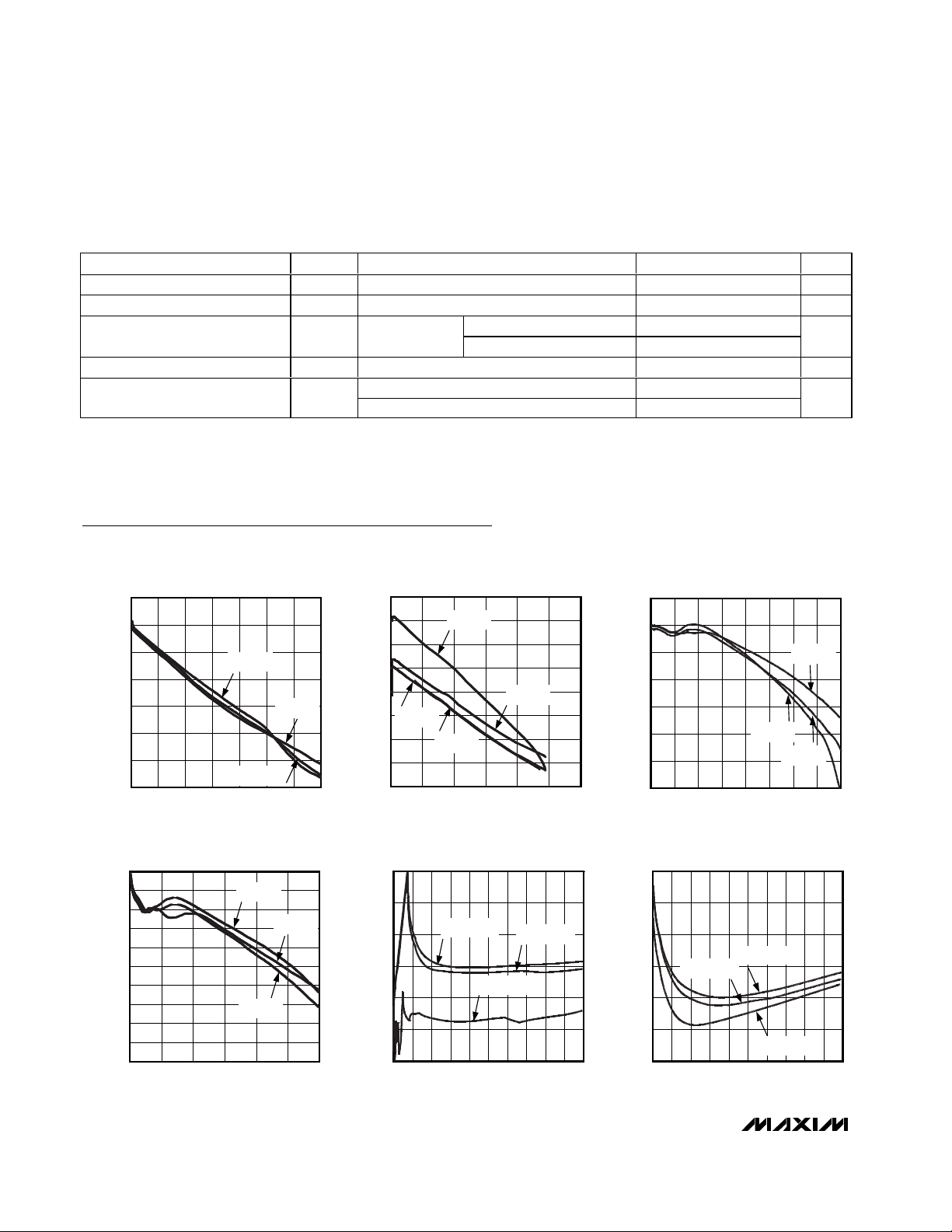
LOAD REGULATION, CIRCUIT 5
MAX1776 toc04
I
LOAD
(A)
V
OUTPUT
(% FROM V
OUT(NOM)
)
VIN = 24V
VIN = 12V
VIN = 15V
-3
0
-1
-2
1
2
3
513117 9 15 17 19 21 23 25
V
OUTPUT
vs. VIN,
CIRCUIT 5, V
OUTPUT
= 5V
MAX1776 toc05
VIN (V)
V
OUTPUT
(%)
I
LOAD
= 1mA
I
LOAD
= 50mA
I
LOAD
= 500mA
-1.0
0.5
0
-0.5
1.0
1.5
2.0
513117 9 15 17 19 21 23 25
V
OUTPUT
vs. VIN,
CIRCUIT 5, V
OUTPUT
= 3.3V
MAX1776 toc06
VIN (V)
V
OUTPUT
(%)
I
LOAD
= 1mA
I
LOAD
= 10mA
I
LOAD
= 50mA
-1.2
-0.8
-1.0
-0.4
-0.6
0
-0.2
0.2
0 200 300100 400 500 600 700
LOAD REGULATION,
CIRCUIT 1, V
OUTPUT
= 5V
MAX1776 toc01
I
LOAD
(mA)
V
OUTPUT
(%)
VIN = 24V
VIN = 12V
VIN = 15V
-1.0
-0.8
-0.6
-0.4
-0.2
0
0.2
0.4
0.6
0200100 300 400 500 600
LOAD REGULATION,
CIRCUIT 1, V
OUTPUT
= 3.3V
MAX1776 toc02
I
LOAD
(mA)
V
OUTPUT
(%)
VIN = 24V
VIN = 12V
VIN = 15V
VIN = 5V
-1.2
-1.0
-0.6
-0.8
-0.2
0
-0.4
0.2
0 100 15050 200 250 300 350 400
LOAD REGULATION, CIRCUIT 2
MAX1776 toc03
I
LOAD
(mA)
V
OUTPUT
(%)
VIN = 24V
VIN = 12V
VIN = 15V
Typical Operating Characteristics
(Circuit of Figure 1, components from Table 3, VIN= +12V, SHDN = IN, TA= +25°C.)
MAX1776
24V, 600mA Internal Switch, 100% Duty Cycle,
Step-Down Converter
4 _______________________________________________________________________________________
ELECTRICAL CHARACTERISTICS (continued)
(Circuit of Figure 1, VIN= +12V, SHDN = IN, TA= -40°C to +85°C, unless otherwise noted.) (Note 1)
Note 1: Specifications to -40°C are guaranteed by design, not production tested.
LX Zero-Crossing Threshold -75 75 mV
LX Switch Leakage Current VIN = 24V, LX = GND 10 µA
Digital Input Level SHDN, ILIM2
Digital Input Leakage Current V
ILIM Input Level
PARAMETER SYMBOL CONDITIONS MIN MAX UNITS
Low 0.8
High 2.4
, V
, V
SHDN
ILIM
= 0 or 24V, VIN = 24V -1 1 µA
ILIM2
Low 0.05
High 2.2
V
V

MAX1776
24V, 600mA Internal Switch, 100% Duty Cycle,
Step-Down Converter
_______________________________________________________________________________________ 5
Typical Operating Characteristics (continued)
(Circuit of Figure 1, components from Table 3, VIN= +12V, SHDN = IN, TA= +25°C.)
V
vs. VIN,
OUTPUT
CIRCUIT 1, V
0.4
0.2
0
(%)
-0.2
OUTPUT
-0.4
V
-0.6
-0.8
1.0
513117 9 15 17 19 21 23 25
I
I
LOAD
LOAD
= 10mA
= 50mA
VIN (V)
EFFICIENCY vs. I
V
100
95
90
85
80
75
70
EFFICIENCY (%)
65
60
55
50
0.10 1 10 100 1000
OUTPUT
VIN = 15V
I
LOAD
OUTPUT
, CIRCUIT 5,
LOAD
= 3.3V
VIN = 6V
VIN = 12V
(mA)
= 5V
I
I
LOAD
VIN = 24V
SWITCHING FREQUENCY vs.
LOAD CURRENT, CIRCUIT 1
200
180
160
140
120
100
80
FREQUENCY (kHz)
60
40
20
0
0 200 300 400100 500 600 700 800 900
VIN = 15V
VIN = 12V
I
LOAD
VIN = 24V
(mA)
LOAD
= 500mA
= 1mA
MAX1776 toc07
MAX1776 toc10
MAX1776 toc13
0.6
0.4
0.2
0
(%)
-0.2
-0.4
OUTPUT
V
-0.6
-0.8
-1.0
-1.2
513117 9 15 17 19 21 23 25
100
95
90
85
80
75
70
EFFICIENCY (%)
65
60
55
50
0.10 1 10 100 1000
140
120
100
80
60
FREQUENCY (kHz)
40
20
0
5 10152025
V
vs. VIN,
OUTPUT
CIRCUIT 1, V
I
LOAD
I
LOAD
EFFICIENCY vs. I
= 10mA
= 50mA
V
OUTPUT
OUTPUT
VIN (V)
VIN = 24V
I
LOAD
I
LOAD
, CIRCUIT 1,
LOAD
= 3.3V
VIN = 6V
(mA)
SWITCHING FREQUENCY vs.
,
CIRCUIT 1
V
IN
I
= 500mA
LOAD
I
= 375mA
LOAD
I
= 250mA
LOAD
I
= 10mA
= 50mA
LOAD
VIN (V)
I
LOAD
= 3.3V
I
LOAD
= 500mA
VIN = 12V
I
LOAD
= 1mA
= 5mA
MAX1776 toc08
MAX1776 toc11
MAX1776 toc14
EFFICIENCY vs. I
V
100
95
90
85
80
75
70
EFFICIENCY (%)
65
60
55
50
0.10 1 10 100 1000
VIN = 6V
VIN = 15V
EFFICIENCY vs. VIN, I
100
95
CIRCUIT 5, 5V
90
85
80
CIRCUIT 1, 3.3V
75
70
EFFICIENCY (%)
65
60
55
50
7 9 10 118 1213141516
V
ACCURACY vs. TEMPERATURE
OUTPUT
1.5
1.0
0.5
0
ACCURACY (%)
OUT
-0.5
V
-1.0
-1.5
-40 20 40-20 0 60 80 100
TEMPERATURE (°C)
I
OUT
LOAD
VIN = 12V
VIN (V)
, CIRCUIT 1,
LOAD
= 5V
VIN = 24V
(mA)
LOAD
CIRCUIT 1, 5V
CIRCUIT 5, 3.3V
MAX1776 toc09
= 500mA
MAX1776 toc12
MAX1776 toc15

MAX1776
24V, 600mA Internal Switch, 100% Duty Cycle,
Step-Down Converter
6 _______________________________________________________________________________________
Typical Operating Characteristics (continued)
(Circuit of Figure 1, components from Table 3, VIN= +12V, SHDN = IN, TA= +25°C.)
15.0
16.0
15.5
17.0
16.5
17.5
18.0
-40 -20 0 20 40 60 80
QUIESCENT SUPPLY CURRENT
vs. TEMPERATURE
MAX1776 toc16
TEMPERATURE (°C)
QUIESCENT SUPPLY CURRENT (µA)
13.70
13.80
13.75
13.90
13.85
14.00
13.95
14.05
14.15
14.10
14.20
5 9 11 1371517192321 25
QUIESCENT SUPPLY CURRENT
vs. SUPPLY VOLTAGE
MAX1776 toc17
SUPPLY VOLTAGE (V)
QUIESCENT SUPPLY CURRENT (µA)
0
0.1
0.2
0.3
0.4
0.5
0.6
0.7
0.8
0 5 10 15 20 25
PEAK SWITCH CURRENT
vs. INPUT VOLTAGE, CIRCUIT 3, 0.3A
MAX1776 toc18
VIN (V)
PEAK SWITCH CURRENT (A)
L = 10µH
L = 22µH
L = 47µH
L = 100µH
LOAD-TRANSIENT RESPONSE,
CIRCUIT 5
MAX1776 toc19
I
LOAD
V
OUT
V
LX
0
1A
0
10V
10µs/div
10mA
500mA
I
L
AC COUPLED
50mV/div
LINE-TRANSIENT RESPONSE,
CIRCUIT 5, I
LOAD
= 500mA
MAX1776 toc20
V
IN
V
OUT
V
LX
AC-COUPLED
200mv/div
5V
10V
200µs/div
0
5V
LINE-TRANSIENT RESPONSE,
CIRCUIT 5, I
LOAD
= 50mA
MAX1776 toc21
V
IN
V
OUT
V
LX
15V
10V
10V
200µs/div
0
5V
AC-COUPLED
200mv/div

MAX1776
24V, 600mA Internal Switch, 100% Duty Cycle,
Step-Down Converter
_______________________________________________________________________________________ 7
Typical Operating Characteristics (continued)
(Circuit of Figure 1, components from Table 3, VIN= +12V, SHDN = IN, TA= +25°C.)
STARTUP WAVEFORM, CIRCUIT 1,
R
LOAD
= 100Ω
MAX1776 toc23
I
L
V
OUT
5V
1A
0
2µs/div
6V
0
V
SHDN
0
2V
4V
75
0.10 100010 1001
EFFICIENCY vs. I
LOAD
, CIRCUIT 3, VIN = 12V
100
85
80
95
90
MAX1776 toc24
I
LOAD
(mA)
EFFICIENCY (%)
L = 22µH
L = 47µH
L = 100µH
75
0.10 100010 1001
EFFICIENCY vs. I
LOAD
, CIRCUIT 3, VIN = 12V
100
85
80
95
90
MAX1776 toc25
I
LOAD
(mA)
EFFICIENCY (%)
L = 22µH, 0.6A
L = 10µH, 1.2A
L = 47µH, 0.3A
LX WAVEFORM, CIRCUIT 1
= 15V, I
V
IN
I
L
V
LX
V
OUT
LOAD
2µs/div
= 500mA
MAX1776 toc22
1A
0
10V
0
50mV/div

MAX1776
24V, 600mA Internal Switch, 100% Duty Cycle,
Step-Down Converter
8 _______________________________________________________________________________________
Detailed Description
The MAX1776 step-down converter is designed primarily for battery-powered devices and notebook computers. The unique current-limited control scheme
provides high efficiency over a wide load range.
Operation up to 100% duty cycle allows the lowest possible dropout voltage, increasing the usable supply
voltage range. Under no load, the MAX1776 draws only
15µA, and in shutdown mode, it draws only 3µA to further reduce power consumption and extend battery life.
Additionally, an internal 24V switching MOSFET, internal current sensing, and a high switching frequency
minimize PC board space and component costs.
Current-Limited Control Architecture
The MAX1776 uses a proprietary current-limited control
scheme with operation to 100% duty cycle. This DC-DC
converter pulses as needed to maintain regulation,
resulting in a variable switching frequency that increases with the load. This eliminates the high supply currents associated with conventional constant-frequency
pulse-width-modulation (PWM) controllers that switch
the MOSFET unnecessarily.
When the output voltage is too low, the error comparator
sets a flip-flop, which turns on the internal P-channel
MOSFET and begins a switching cycle (Figure 2). As
shown in Figure 3, the inductor current ramps up linearly, storing energy in a magnetic field while charging the
output capacitor and servicing the load. The MOSFET
turns off when the peak current limit is reached, or when
the maximum on-time of 10µs is exceeded and the output voltage is in regulation. If the output is out of regulation and the peak current is never obtained, the
MOSFET remains on, allowing a duty cycle up to 100%.
This feature ensures the lowest possible dropout voltage. Once the MOSFET turns off, the flip-flop resets, the
inductor current is pulled through D1, and the current
through the inductor ramps back down, transferring the
stored energy to the output capacitor and load. The
MOSFET remains off until the 0.42µs minimum off-time
expires, and the output voltage drops out of regulation.
Pin Description
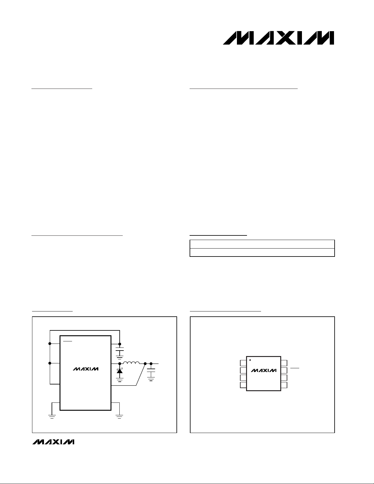
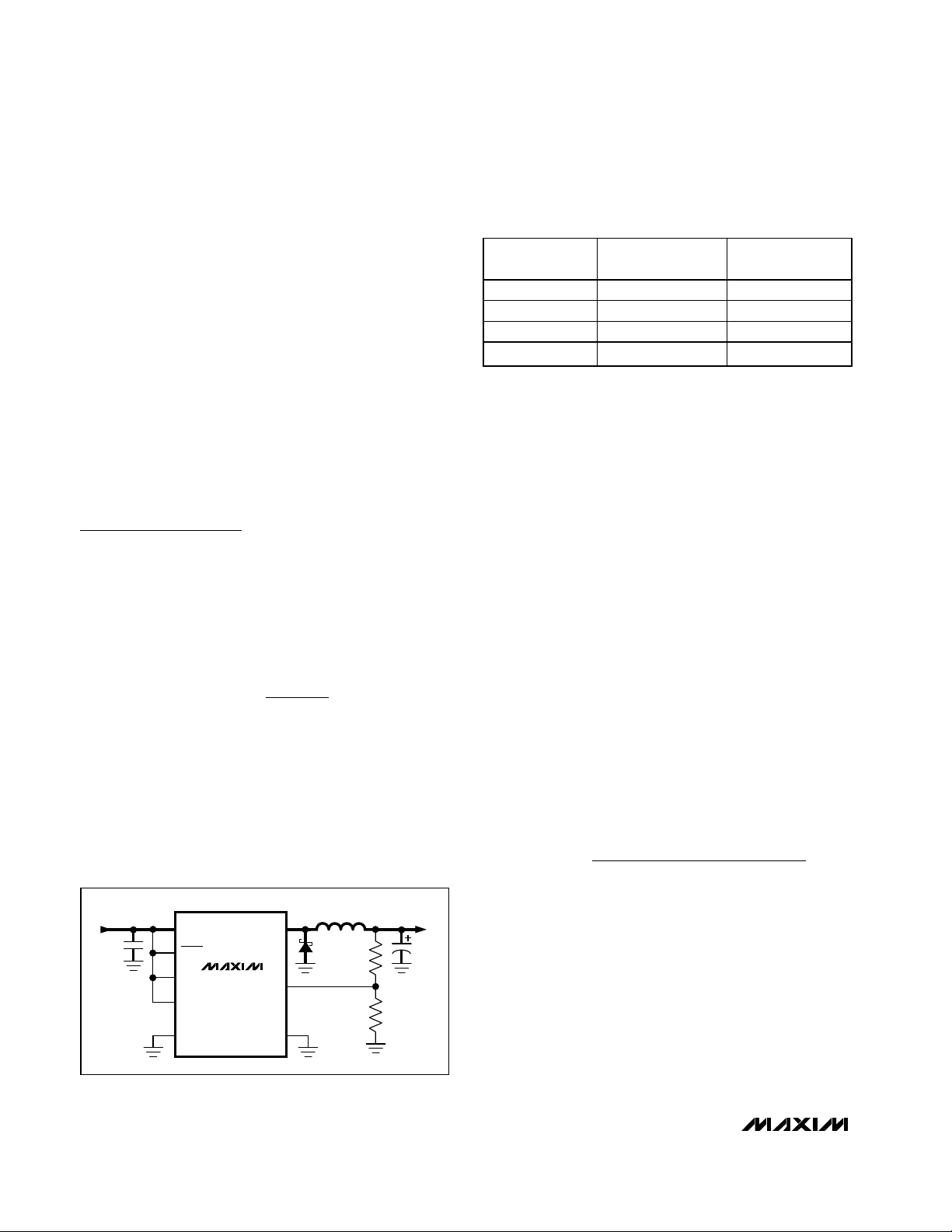
Figure 1. Typical Application Circuit
PIN NAME FUNCTION
1FB
2 GND Ground
3 ILIM
4 LX Inductor Connection. Connect LX to external inductor and diode as shown in Figure 1.
5 IN Input Supply Voltage. Input voltage range is 4.5V to 24V.
6 ILIM2
7 SHDN
8 OUT
Dual-Mode Feedback Input. Connect to GND for the preset 5V output. Connect to a resistive divider
between OUT and GND to adjust the output voltage between 1.25V and V
Peak Current Control Input. Connect to IN or GND to set peak current limit. ILIM and ILIM2 together set
the peak current limit. See Setting Current Limit.
Peak Current Control Input 2. Connect to IN or GND. ILIM and ILIM2 together set the peak current limit.
See Setting Current Limit.
Shutdown Input. A logic low shuts down the MAX1776 and reduces the supply current to 3µA. LX is high
impedance in shutdown. Connect to IN for normal operation.
Regulated Output Voltage High-Impedance Sense Input. Internally connected to a resistive divider.
Do not connect for output voltages higher than 5.5V. Connect to GND when not used.
INPUT
4.5V TO 24V
C
IN
J1
J2
CIN: 10µF, 25V CERAMIC
SEE TABLE 3 FOR OTHER COMPONENT VALUES
IN
SHDN
MAX1776
ILIM
J3
ILIM2
J4
GND
NOTE: HIGH-CURRENT PATHS SHOWN WITH BOLD LINES.
LX
OUT
FB
L1
D1
OUTPUT
C
OUT
.
IN
5V

MAX1776
24V, 600mA Internal Switch, 100% Duty Cycle,
Step-Down Converter
_______________________________________________________________________________________ 9
Input-Output (Dropout) Voltage
A step-down converter’s minimum input-to-output voltage differential (dropout voltage) determines the lowest
usable supply voltage. In battery-powered systems,
this limits the useful end-of-life battery voltage. To maximize battery life, the MAX1776 operates with duty
cycles up to 100%, which minimizes the dropout voltage and eliminates switching losses while in dropout.
When the supply voltage approaches the output voltage, the P-channel MOSFET remains on continuously to
supply the load.
Dropout voltage is defined as the difference between
the input and output voltages when the input is low
enough for the output to drop out of regulation. For a
step-down converter with 100% duty cycle, dropout
depends on the MOSFET drain-to-source on-resistance
and inductor series resistance; therefore, it is proportional to the load current:
V
DROPOUT
= I
OUT
✕
(R
DS(ON) + RINDUCTOR
)
Figure 2. Simplified Functional Diagram
Figure 3. Discontinuous-Conduction Operation
D
C
IN
SHDN
ILIM
ILIM2
ILIM
SET
MAXIMUM
ON-TIME
DELAY
MINIIMUM
OFF-TIME
DELAY
MAX1776
RQ
S
100mV
V
SET
1.25V
OUT
FB
GND
L1
LX
D1
OUTPUT
C
OUT
LX WAVEFORM, CIRCUIT 1
= 15V, I
V
IN
I
L
V
LX
V
OUT
LOAD
2µs/div
= 500mA
1A
0
10V
0
50mV/div
MAX1776
24V, 600mA Internal Switch, 100% Duty Cycle,
Step-Down Converter
10 ______________________________________________________________________________________
Shutdown (
SSHHDDNN
)
A logic low level on SHDN shuts down the MAX1776
converter. When in shutdown, the supply current drops
to 3µA to maximize battery life, and the internal P-channel MOSFET turns off to isolate the output from the input.
The output capacitance and load current determine the
rate at which the output voltage decays. A logic level
high on SHDN activates the MAX1776. Do not leave
SHDN floating. If unused, connect SHDN to IN.
Thermal-Overload Protection
Thermal-overload protection limits total power dissipation in the MAX1776. When the junction temperature
exceeds T
J
= +160°C, a thermal sensor turns off the
pass transistor, allowing the IC to cool. The thermal sensor turns the pass transistor on again after the IC’s junction temperature cools by 10°C, resulting in a pulsed
output during continuous thermal-overload conditions.
Design Information
Output Voltage Selection
The feedback input features dual-mode operation.
Connect FB to GND for the 5.0V preset output voltage.
Alternatively, adjust the output voltage by connecting a
voltage-divider from the output to GND (Figure 4).
Select a value for R2 between 10kΩ and 100kΩ.
Calculate R1 with the following equation:
where VFB= 1.25V, and V
OUTPUT
may range from
1.25V to VIN.
Setting Current Limit
The MAX1776 has an adjustable peak current limit.
Configure this peak current limit by connecting ILIM
and ILIM2 as shown in Table 1.
Choose a current limit that realistically reflects the maximum load current. The maximum output current is half
of the peak current limit. Although choosing a lower
current limit allows using an inductor with a lower current rating, it requires a higher inductance (see
Inductor Selection) and does little to reduce inductor
package size.
Inductor Selection
When selecting the inductor, consider these four parameters: inductance value, saturation rating, series
resistance, and size. The MAX1776 operates with a
wide range of inductance values. For most applications, values between 10µH and 100µH work best with
the controller’s high switching frequency. Larger inductor values will reduce the switching frequency and
thereby improve efficiency and EMI. The trade-off for
improved efficiency is a higher output ripple and slower
transient response. On the other hand, low-value inductors respond faster to transients, improve output ripple,
offer smaller physical size, and minimize cost. If the
inductor value is too small, the peak inductor current
exceeds the current limit due to current-sense comparator propagation delay, potentially exceeding the
inductor’s current rating. Calculate the minimum inductance value as follows:
where t
ON(MIN)
= 1µs.
The inductor’s saturation current rating must be greater
than the peak switch current limit, plus the overshoot
due to the 250ns current-sense comparator propagation delay. Saturation occurs when the inductor’s magnetic flux density reaches the maximum level the core
can support and the inductance starts to fall. Choose
an inductor with a saturation rating greater than I
PEAK
in the following equation:
I
PEAK
= I
LX(PEAK)
+ (VIN- V
OUTPUT
) ✕250ns / L
Figure 4. Adjustable Output Voltage
Table 1. Current-Limit Configuration
R1 R2
V
OUTPUT
V
FB
-=×
1
CURRENT
LIMIT (mA)
150 GND GND
300 GND IN
600 IN GND
1200 IN IN
ILIM
CONNECTED TO
CONNECTED TO
L
(MIN) =
VV
()
IN(MAX) OUTPUT ON(MIN)
-
I
LX (PEAK
× t
)
ILIM2
R1
R2
OUTPUT
1.25V TO V
IN
C
OUT
INPUT
4.5V TO 24V
C
IN
IN
SHDN
ILIM
ILIM2
GND
MAX1776
LX
L1
D1
FB
OUT

Inductor series resistance affects both efficiency and
dropout voltage (see Input-Output (Dropout) Voltage).
High series resistance limits the maximum current available at lower input voltages, and increases the dropout
voltage. For optimum performance, select an inductor
with the lowest possible DC resistance that fits in the
allotted dimensions. Some recommended component
manufacturers are listed in Table 2.
Maximum Output Current
The MAX1776 converter’s output current determines
the regulator’s switching frequency. When the converter approaches continuous mode, the output voltage
falls out of regulation. For the typical application, the
maximum output current is approximately:
I
LOAD(MAX)
= 1/2 I
LX (PEAK)(MIN)
For low-input voltages, the maximum on-time may be
reached and the load current is limited by:
I
LOAD
= 1/2 (VIN- V
OUT
) ✕10µs / L
Output Capacitor
Choose the output capacitor to service the maximum
load current with acceptable voltage ripple. The output
ripple has two components: variations in the charge
stored in the output capacitor with each LX pulse, and
the voltage drop across the capacitor’s equivalent
series resistance (ESR) caused by the current into and
out of the capacitor:
V
RIPPLE
≅ V
RIPPLE(ESR)
+ V
RIPPLE(C)
The output voltage ripple as a consequence of the ESR
and output capacitance is:
where I
PEAK
is the peak inductor current (see Inductor
Selection). The worst-case ripple occurs at no-load.
These equations are suitable for initial capacitor selection, but final values should be set by testing a prototype or evaluation circuit. As a general rule, a smaller
amount of charge delivered in each pulse results in
less output ripple. Since the amount of charge delivered in each oscillator pulse is determined by the
inductor value and input voltage, the voltage ripple
increases with larger inductance, and as the input voltage decreases. See Table 3 for recommended capacitor values and Table 2 for recommended component
manufacturers.
Input Capacitor
The input filter capacitor reduces peak currents drawn
from the power source and reduces noise and voltage
ripple on the input caused by the circuit’s switching.
The input capacitor must meet the ripple-current
requirement (I
RMS
) imposed by the switching current
defined by the following equation:
For most applications, nontantalum chemistries (ceramic, aluminum, polymer, or OS-CON) are preferred due to
their robustness to high inrush currents typical of systems with low-impedance battery inputs. Alternatively,
connect two (or more) smaller value low-ESR capacitors
in parallel to reduce cost. Choose an input capacitor
that exhibits less than +10°C temperature rise at the
RMS input current for optimal circuit longevity.
MAX1776
24V, 600mA Internal Switch, 100% Duty Cycle,
Step-Down Converter
______________________________________________________________________________________ 11
Table 2. Component Suppliers
V
RIPPLE(ESR) PEAK
V
RIPPLE(C)
ESR I
=×
LI I
×
=
C
2VVVV
-
()
PEAK OUTPUT
×
OUT OUTPUT
2
IN OUTPUT
IN
-
IV
I
LOAD OUTPUT
=×−
RMS
V
IN
4
V
3
IN
V
OUTPUT
1
SUPPLIER WEBSITE
DIODES
Central Semiconductor www.centralsemi.com
Fairchild www.fairchildsemi.com
General Semiconductor www.gensemi.com
International Rectifier www.irf.com
Nihon
On Semi www.onsemi.com
Vishay-Siliconix
Zetex
CAPACITORS
AVX www.avxcorp.com
Kemet www.kemet.com
Nichicon www.nichicon-us.com
Sanyo www.sanyo.com
Taiyo Yuden www.t-yuden.com
INDUCTORS
Coilcraft www.coilcraft.com
Coiltronics www.cooperet.com
Pulse Engineering www.pulseeng.com
Sumida USA www.sumida.com
Toko www.tokoam.com
www.niec.co.jp/engver2/
niec.co.jp_eg.htm
www.vishay.com/brands/siliconix/
main.html
www.zetex.com

MAX1776
Diode Selection
The current in the external diode (D1 in Figure 1)
changes abruptly from zero to its peak value each time
the LX switch turns off. To avoid excessive losses, the
diode must have a fast turn-on time and a low forward
voltage.
Make sure that the diode’s peak current rating exceeds
the peak current limit set by the current limit, and that
its breakdown voltage exceeds VIN. Use Schottky
diodes when possible.
MAX1776 Stability
Instability is frequently caused by excessive noise on
OUT, FB, or GND due to poor layout or improper component selection. Instability typically manifests itself as
“motorboating,” which is characterized by grouped
switching pulses with large gaps and excessive lowfrequency output ripple during no-load or light-load
conditions.
PC Board Layout and Grounding
High switching frequencies and large peak currents
make PC board layout an important part of the design.
Poor layout introduces switching noise into the feedback path, resulting in jitter, instability, or degraded
performance. High-power traces, highlighted in the
24V, 600mA Internal Switch, 100% Duty Cycle,
Step-Down Converter
12 ______________________________________________________________________________________
Table 3. Recommended Components
INPUT
CIRCUIT
1 10 to 24 600 1.20
2 10 to 24 300 0.60
3 10 to 24 150 0.30
4 10 to 24 75 0.15
5 5 to 15 600 1.20
6 5 to 15 300 0.60
7 5 to 15 150 0.30
8 5 to 15 75 0.15
VOLTAGE
(V)
MAXIMUM
LOAD
CURRENT
(mA)
I
LX(PEAK)
CURRENT
(A)
INDUCTOR CAPACITOR
10µH, 1.56A, 70mΩ
Toko D75F 646FY-100M,
10µH, 1.70A, 48mΩ
Sumida CDRH6D28-100NC,
or 10µH, 1.63A, 55mΩ
Toko D75C 646CY-100M 0.055
22µH, 1.17A, 120mΩ
Toko D75F 646FY-220M,
22µH, 1.09A, 115mΩ
Toko D75C 646CY-220M,
or 22µH, 1.20A, 95mΩ
Sumida CDRH6D28-220NC
47µH, 0.54A, 440mΩ
Sumida CDRH5D18-470
100µH, 0.29A, 766mΩ
Sumida CDRH4D28-101
5.4µH, 1.6A, 56mΩ
Sumida CDRH5D18-5R4
10µH, 1.04A, 80mΩ
Toko D73LC 817CY-100M
22µH, 0.41A, 294mΩ
Sumida CDRH4D18-220
47µH, 0.33A, 230mΩ
Coilcraft DS1608C-473
100µF, 6.3V
Sanyo POSCAP 6TPC100M
47µF, 6.3V
Sanyo POSCAP 6TPA47M
22µF, 6.3V, 1210 case
Taiyo Youden JMK325BJ226MM
10µF, 6.3V, X7R, 1206 case
Taiyo Youden JMK316BJ106ML
100µF, 6.3V
Sanyo POSCAP 6TPC100m
47µF, 6.3V
Sanyo POSCAP 6TPA47M
22µF, 6.3V, 1210 case
Taiyo Youden JMK325BJ226MM
10µF, 6.3V, X7R, 1206 case
Taiyo Youden JMK316BJ106ML
MAX1776
24V, 600mA Internal Switch, 100% Duty Cycle,
Step-Down Converter
Maxim cannot assume responsibility for use of any circuitry other than circuitry entirely embodied in a Maxim product. No circuit patent licenses are
implied. Maxim reserves the right to change the circuitry and specifications without notice at any time.
Maxim Integrated Products, 120 San Gabriel Drive, Sunnyvale, CA 94086 408-737-7600 ____________________ 13
© 2003 Maxim Integrated Products Printed USA is a registered trademark of Maxim Integrated Products.
Typical Application Circuit (Figure 1), should be as
short and wide as possible. Additionally, the current
loops formed by the power components (CIN, COUT,
L1, and D1) should be as short as possible to avoid
radiated noise. Connect the ground pins of these
power components at a common node in a star-ground
configuration. Separate the noisy traces, such as the
LX node, from the feedback network with grounded
copper. Furthermore, keep the extra copper on the
board and integrate it into a pseudo-ground plane.
When using external feedback, place the resistors as
close to the feedback pin as possible to minimize noise
coupling.
Chip Information
TRANSISTOR COUNT: 932
PROCESS: BiCMOS
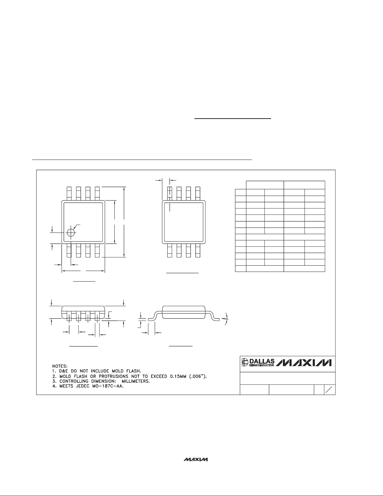
Package Information
4X S
BOTTOM VIEW
0.6±0.1
0.6±0.1
8
1
TOP VIEW
ÿ 0.50±0.1
D
E H
8
1
DIM
A
A1
A2
b
c
D
e
E
H
L
α
S
INCHES
MIN
-
0.002
0.030
0.010
0.005
0.116
0.0256 BSC
0.116
0.188
0.016
0∞
0.0207 BSC
MAX
0.043
0.006
0.037
0.014
0.007
0.120
0.120
0.198
0.026
6∞
MILLIMETERS
MIN
0.05 0.15
0.25 0.36
0.13 0.18
2.95 3.05
2.95 3.05
4.78
0.41
MAX
- 1.10
0.950.75
0.65 BSC
5.03
0.66
0.5250 BSC
6∞0∞
8LUMAXD.EPS
A2
e
FRONT VIEW
A1
A
c
b
L
SIDE VIEW
α
PROPRIETARY INFORMATION
TITLE:
PACKAGE OUTLINE, 8L uMAX/uSOP
REV.DOCUMENT CONTROL NO.APPROVAL
21-0036
1
J
1
 Loading...