

Page 1
General Description
The MAX1772 is a highly-integrated, multichemistry
battery-charger control IC that simplifies the construction of accurate and efficient chargers. The MAX1772
uses analog inputs to control charge current and voltage and can be programmed by the host or hardwired.
High efficiency is achieved by a buck topology with
synchronous rectification.
Maximum current drawn from the AC adapter is programmable to avoid overloading the AC adapter when
supplying the load and the battery charger simultaneously. This enables the user to reduce the cost of the
AC adapter. The MAX1772 provides outputs that can
be used to monitor the current drawn from the AC
adapter, battery-charging current, and the presence of
an AC adapter.
The MAX1772 can charge two to four lithium-ion (Li+)
series cells, easily providing 4A. When charging, the
MAX1772 automatically transitions from regulating current to regulating voltage. It is available in a space-saving 28-pin QSOP package.
Applications
Notebook and Subnotebook Computers
Personal Digital Assistants
Handheld Terminals
Features
♦ Input Current Limiting
♦ ±0.5% Output Voltage Accuracy Using Internal
Reference (0°C to +85°C)
♦ Programmable Battery Charge Current >4A
♦ Analog Inputs Control Charge Current and
Charge Voltage
♦ Monitor Outputs for:
Current Drawn from AC Input Source
Charging Current
AC Adapter Present
♦ Up to 18.2V (max) Battery Voltage
♦ 8V to 28V Input Voltage
♦ >95% Efficiency
♦ 99.99% (max) Duty Cycle for Low-Dropout
Operation
♦ Charges Any Battery Chemistry: Li+, NiCd, NiMH,
Lead Acid, etc.
MAX1772
Low-Cost, Multichemistry Battery-
Charger Building Block
________________________________________________________________ Maxim Integrated Products 1
28
27
26
25
24
23
22
21
20
19
18
17
16
15
1
2
3
4
5
6
7
8
9
10
11
12
13
14
IINP
CSSP
CSSN
BST
DHI
LX
VCTL
DLOV
DLO
PGND
CSIP
CSIN
BATT
CELLS
ICTL
REFIN
ACOK
ACIN
ICHG
GND
GND
CCV
CCI
CCS
REF
CLS
LDO
DCIN
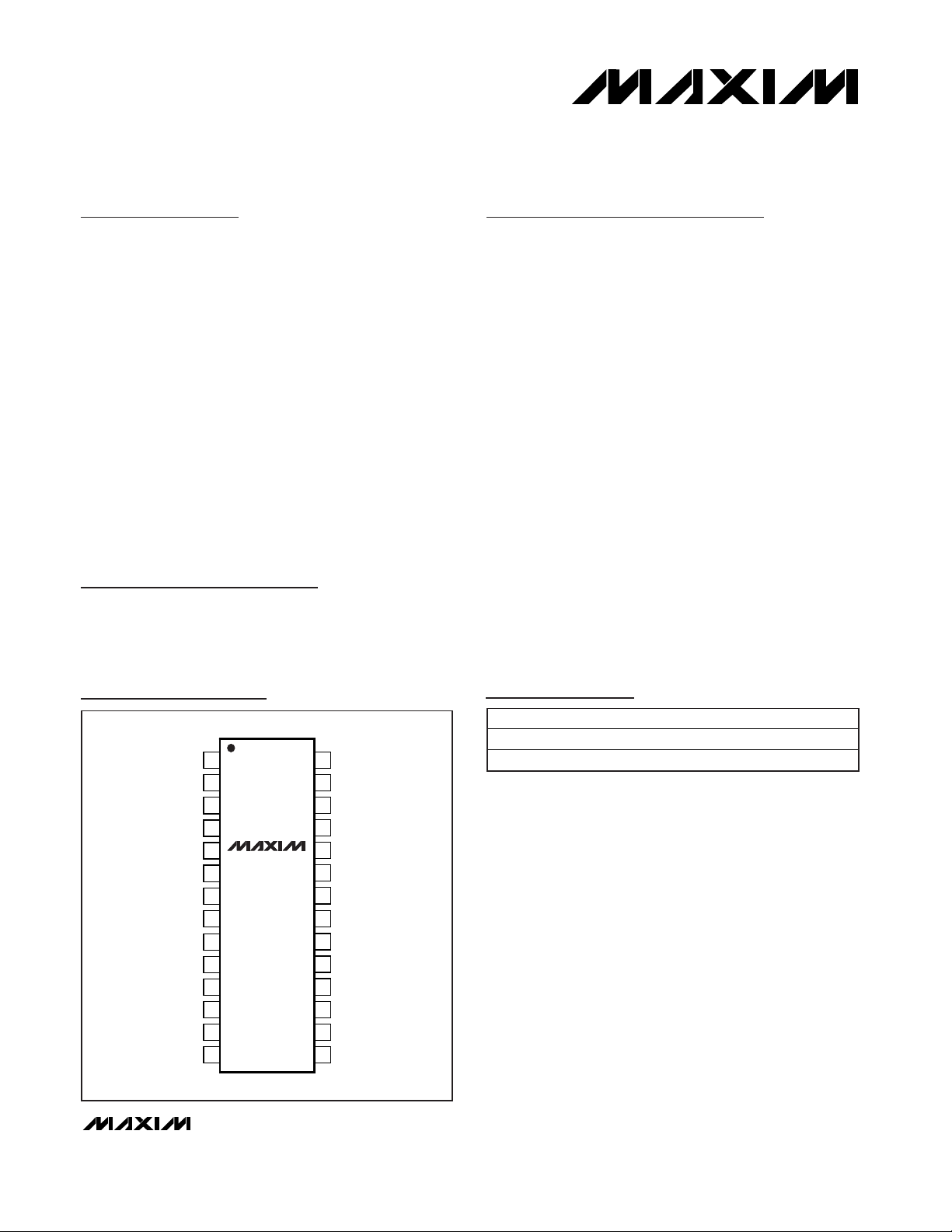
QSOP
TOP VIEW
MAX1772
Pin Configuration
19-1772; Rev 3; 8/05
Ordering Information
PART
TEMP RANGE
PIN-PACKAGE
MAX1772EEI -40°C to +85°C 28 QSOP
MAX1772EEI+ -40°C to +85°C 28 QSOP
For pricing, delivery, and ordering information, please contact Maxim/Dallas Direct! at
1-888-629-4642, or visit Maxim’s website at www.maxim-ic.com.
+Denotes lead-free package.
Page 2
MAX1772
Low-Cost, Multichemistry BatteryCharger Building Block
2 _______________________________________________________________________________________
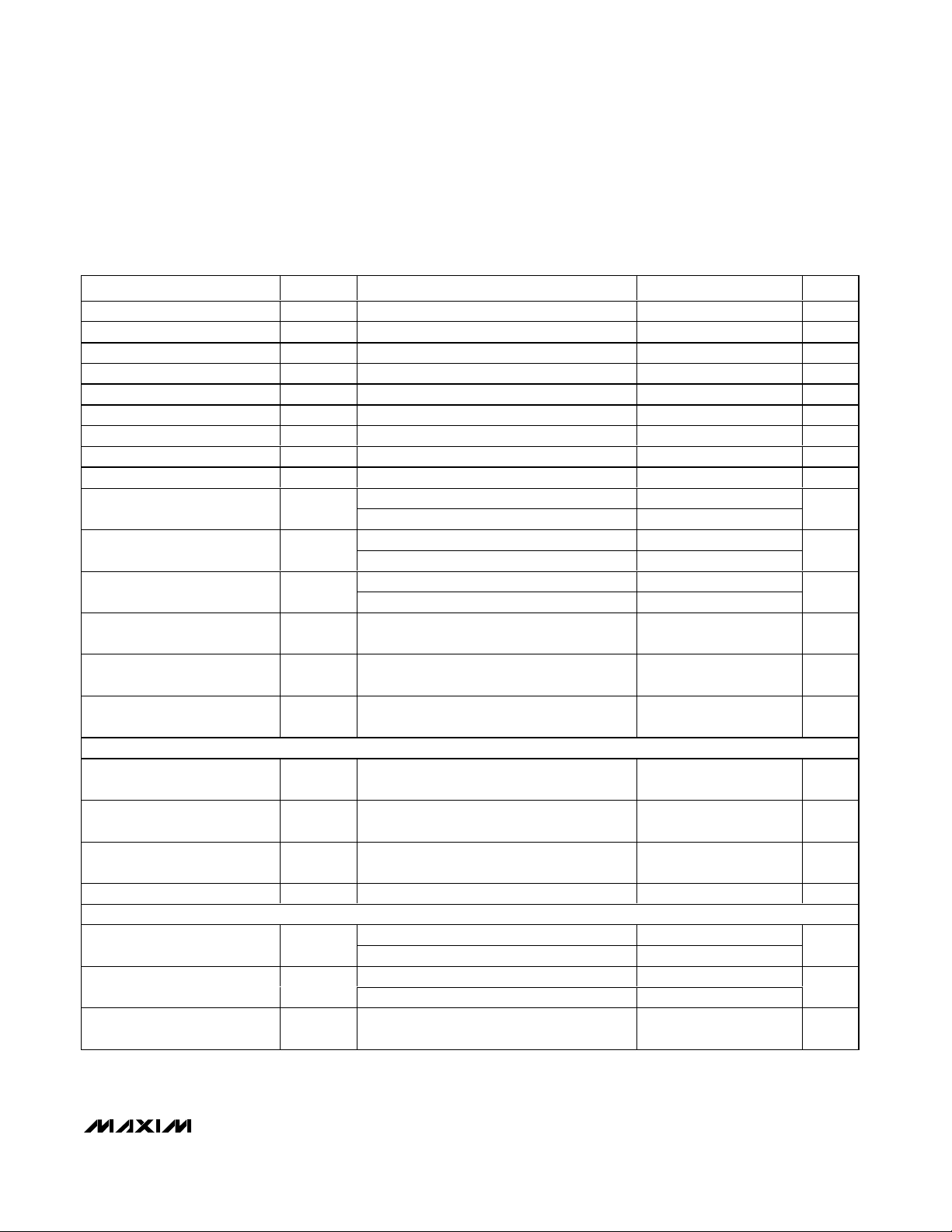
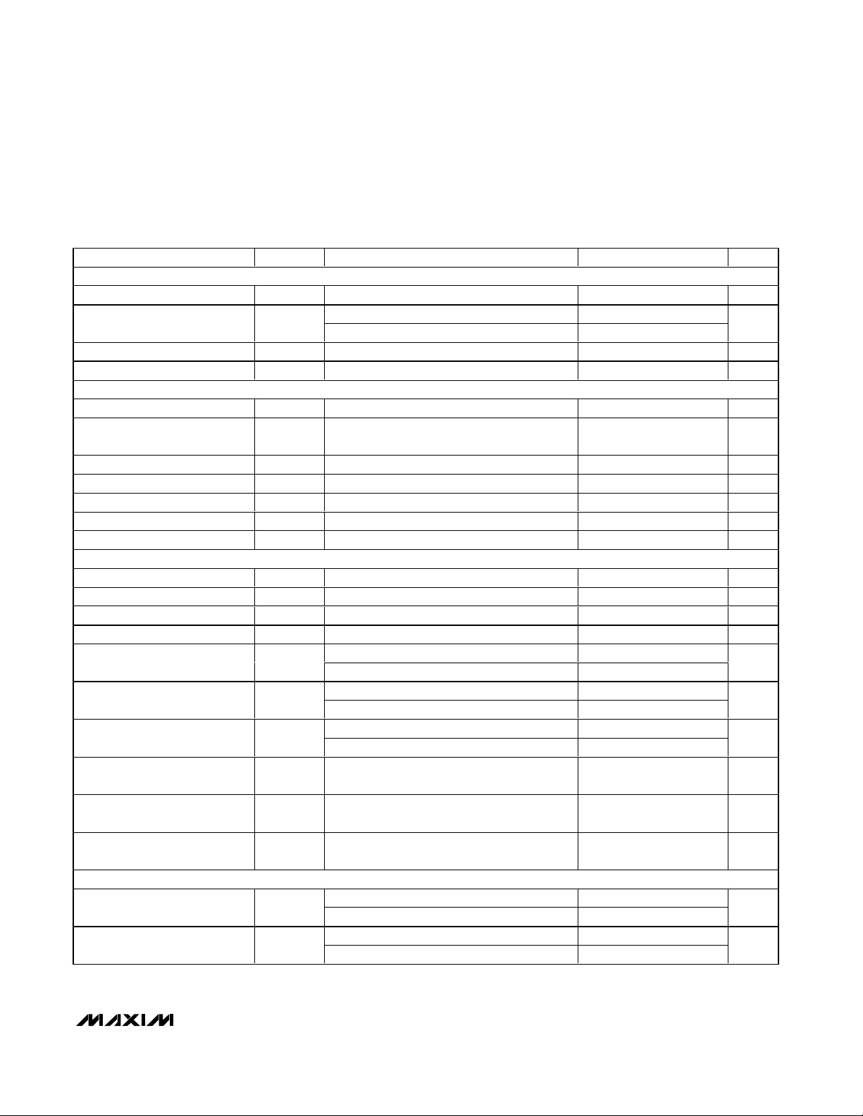
ABSOLUTE MAXIMUM RATINGS
ELECTRICAL CHARACTERISTICS
(V
DCIN
= V
CSSP
= V
CSSN
= 18V, V
BATT
= V
CSIP
= V
CSIN
= 12V, V
REFIN
= 3.0V, V
VCTL
= V
ICTL
= 0.75 ✕REFIN, CELLS = 2.0V,
ACIN = 0, CLS = REF, V
BST
- VLX= 4.5V, GND = PGND = 0, C
LDO
= 1µF, LDO = DLOV, C
REF
= 1µF; pins CCI, CCS, and CCV are
compensated per Figure 1a; T
A
= 0°C to +85°C, unless otherwise noted. Typical values are at TA= +25°C.)
Stresses beyond those listed under “Absolute Maximum Ratings” may cause permanent damage to the device. These are stress ratings only, and functional
operation of the device at these or any other conditions beyond those indicated in the operational sections of the specifications is not implied. Exposure to
absolute maximum rating conditions for extended periods may affect device reliability.
DCIN, CSSP, CSSN to GND ...................................-0.3V to +30V
BST to GND ............................................................-0.3V to +36V
BST to LX..................................................................-0.3V to +6V
DHI to LX ....................................................-0.3V to (BST + 0.3V)
LX to GND .................................................................-6V to +30V
BATT, CSIP, CSIN to GND........................................-0.3V to 20V
CSIP to CSIN or CSSP to CSSN or
PGND to GND ...........……….……………..…….-0.3V to +0.3V
CCI, CCS, CCV, DLO, ICHG, IINP,
ACIN, REF to GND ..............................-0.3V to (VLDO + 0.3V)
DLOV, VCTL, ICTL, REFIN, CELLS,
CLS, LDO, ACOK to GND ....................................-0.3V to +6V
DLOV to LDO.........................................................-0.3V to +0.3V
DLO to PGND ..........................................-0.3V to (DLOV + 0.3V)
LDO Short-Circuit Current ..................................................50mA
Continuous Power Dissipation (T
A
= +70°C)
28-Pin QSOP (derate 10.8mW/°C above +70°C).........860mW
Operating Temperature Range
MAX1772EEI....................................................-40°C to +85°C
Junction Temperature ........................................................150°C
Storage Temperature Range .............................-60°C to +150°C
Lead Temperature (soldering, 10s) .................................+300°C
PARAMETER
CONDITIONS
UNITS
SUPPLY AND LDO REGULATOR
DCIN Input Voltage Range
V
DCIN
8 28 V
DCIN falling 7.0 7.4
DCIN Undervoltage Lockout
Trip Point
DCIN rising 7.5
V
DCIN Quiescent Current
I
DCIN
8.0V < V
DCIN
< 28V
2.7 6.0 mA
LDO Output Voltage
8.0V < V
DCIN
< 28V, no load
V
LDO Load Regulation
0 < I
LDO
< 10mA
34
mV
LDO Undervoltage Lockout
Trip Point
V
DCIN
= 8.0V
V
REF Output Voltage
0 < I
REF
< 500µA
V
REF Undervoltage Lockout
Trip Point
REF falling 3.1 3.9 V
TRIP POINTS
BATT POWER_FAIL Threshold
V
CSSP
falling
50 100
mV
BATT POWER_FAIL Threshold
Hysteresis
200
mV
ACIN Threshold ACIN rising
V
ACIN Threshold Hysteresis 0.5% of REF 10 20 30 mV
ACIN Input Bias Current
V
ACIN
= 2.048V
-1 +1 µA
CLS Input Range 1.6
V
CLS Input Bias Current
V
CLS
= 2.0V
-1 +1 µA
SWITCHING REGULATOR
Minimum Off-Time
V
BATT
=16.8V
µs
Maximum On-Time 5 10 15 ms
Oscillator Frequency
f
OSC
(Note 1)
kHz
SYMBOL
MIN TYP MAX
5.25 5.40 5.55
3.20 4.00 5.15
4.072 4.096 4.120
100
2.007 2.048 2.089
1.00 1.25 1.50
7.85
100
150
300
REF
400
Page 3
MAX1772
Low-Cost, Multichemistry Battery-
Charger Building Block
_______________________________________________________________________________________ 3
ELECTRICAL CHARACTERISTICS (continued)
(V
DCIN
= V
CSSP
= V
CSSN
= 18V, V
BATT
= V
CSIP
= V
CSIN
= 12V, V
REFIN
= 3.0V, V
VCTL
= V
ICTL
= 0.75 ✕REFIN, CELLS = 2.0V,
ACIN = 0, CLS = REF, V
BST
- VLX= 4.5V, GND = PGND = 0, C
LDO
= 1µF, LDO = DLOV, C
REF
= 1µF; pins CCI, CCS, and CCV are
compensated per Figure 1a; T
A
= 0°C to +85°C, unless otherwise noted. Typical values are at TA= +25°C.)
PARAMETER
CONDITIONS
UNITS
DLOV Supply Current
I
DLOV
DLO low 5 10 µA
BST Supply Current
I
BST
DHI high 6 15 µA
LX Input Bias Current
V
DCIN
= 28V, V
BATT
= VLX = 20V
150
µA
LX Input Quiescent Current
V
DCIN
= 0, V
BATT
= VLX = 20V
0.3 1.0 µA
DHI Maximum Duty Cycle
%
DHI On-Resistance High
V
BST
- VLX = 4.5V, I
DHI
= +100mA
4 7 Ω
DHI On-Resistance Low
V
BST
- VLX = 4.5V, I
DHI
= -100mA
1 2 Ω
DLO On-Resistance High
V
DLOV
= 4.5V, I
DLO
= +100mA
4 7 Ω
DLO On-Resistance Low
V
DLOV
= 4.5V, I
DLO
= -100mA
1 2 Ω
V
BATT
= 19V, V
DCIN
= 0
5
BATT Input Current
I
BATT
V
BATT
= 2V to 19V, V
DCIN
> V
BATT
+ 0.3V
200
µA
V
DCIN
= 0
1 5
CSIP/CSIN Input Current
V
CSIP
= V
CSIN
= 12V
µA
V
DCIN
= 0
0.1 0.3
CSSP/CSSN Input Current
V
CSSP
= V
CSSN
= V
DCIN
> 8.0V
µA
BATT/CSIP/CSIN Input Voltage
Range
0 19 V
CSIP to CSIN Full-Scale
Current-Sense Voltage
V
BATT
= 12V
204
mV
CSSP to CSSN Full-Scale
Current-Sense Voltage
204
mV
ERROR AMPLIFIERS
GMV Amplifier
Transconductance
V C TL = RE FIN , V
BAT T
= 16.8V , C E LLS = LD O
µS
GMI Amplifier
Transconductance
ICTL = REFIN, V
CSIP
- V
CSIN
= 150.4mV
0.5 1 2 µS
GMS Amplifier
Transconductance
V
CLS
= 2.048V, V
CSSP
- V
CSSN
= 102.4mV
0.5 1 2 µS
CCI/CCS/CCV Clamp Voltage
0.25V < V
CCV/S/I
< 2.0V
300
mV
CURRENT AND VOLTAGE SETTING
ICTL = REFIN (see Equation 2) -8 +8
Charging-Current Accuracy
ICTL = REFIN/32 (see Equation 2) -55
%
V
VCTL
= V
ICTL
= V
REFIN
= 3V
-1 +1
ICTL, VCTL, REFIN Input Bias
Current
V
DCIN
= 0, V
VCTL
= V
ICTL
= V
REFIN
= 5V
-1 +1
µA
ICTL Power-Down Mode
Threshold Voltage
REFIN
REFIN
/55
REFIN
/33
V
SYMBOL
MIN TYP MAX
500
99.0 99.9
500
800
800
189
189
0.0625 0.1250 0.250
219
219
150
/100
600
+55
Page 4
MAX1772
Low-Cost, Multichemistry BatteryCharger Building Block
4 _______________________________________________________________________________________
ELECTRICAL CHARACTERISTICS (continued)
(V
DCIN
= V
CSSP
= V
CSSN
= 18V, V
BATT
= V
CSIP
= V
CSIN
= 12V, V
REFIN
= 3.0V, V
VCTL
= V
ICTL
= 0.75 ✕REFIN, CELLS = 2.0V,
ACIN = 0, CLS = REF, V
BST
- VLX= 4.5V, GND = PGND = 0, C
LDO
= 1µF, LDO = DLOV, C
REF
= 1µF; pins CCI, CCS, and CCV are
compensated per Figure 1a; T
A
= 0°C to +85°C, unless otherwise noted. Typical values are at TA= +25°C.)
PARAMETER
CONDITIONS
UNITS
V
VCTL
= V
REFIN
(2, 3, or 4 cells)
(see Equation 1)
Battery-Regulation Voltage
Accuracy
V
VCTL
= V
REFIN
/20 (2, 3, or 4 cells)
(see Equation 1)
%
REFIN Range 2.0 3.6 V
REFIN Undervoltage Lockout
V
ICHG Transconductance
V
ICHG
to (V
CSIP
- V
CSIN
); V
CSIP
-
V
CSIN
= 0.185V; V
ICHG
= 0, 3.0V
µS
V
CSIP
- V
CSIN
= 0.185V
-5 +5
ICHG Accuracy
V
CSIP
- V
CSIN
= 0.05V
-10
%
IINP Transconductance
V
IINP
to (V
CSSP
- V
CSSN
); V
CSSP
-
V
CSSN
= 0.185V; V
IINP
= 0, 3.0V (Note 2)
µS
V
CSSP
- V
CSSN
= 0.185V
-15
IINP Current Accuracy
V
CSSP
- V
CSSN
= 0.05V
(Note 2)
-20
%
V
CSSP
- V
CSSN
= 0.08V, V
CLS
= 1.6V
-10
CSSP - CSSN Accuracy
V
CSSP
- V
CSSN
= 0.2V, CLS = REF
-10
%
CSSP + CSSN Input Voltage
Range
8.0 28 V
LOGIC LEVELS
CELLS Input Low Voltage 0.2 V
CELLS Input Middle Voltage 0.4
V
LDO
V
CELLS Input High Voltage
V
LDO
V
CELLS Input Bias Current
CELLS = 0 or V
LDO
-10
µA
ACOK Sink Current
V
ACOK
= 0.4V
1 mA
ACOK Leakage Current
V
ACOK
= 5.5V
-1 +1 µA
SYMBOL
MIN TYP MAX
-0.5
-0.5
1.20 1.92
0.95 1.00 1.05
0.85 1.00 1.15
- 0.25
+0.5
+0.5
+10
+15
+20
+10
+10
- 0.5
V
LDO
+10
Page 5
MAX1772
Low-Cost, Multichemistry Battery-
Charger Building Block
_______________________________________________________________________________________ 5
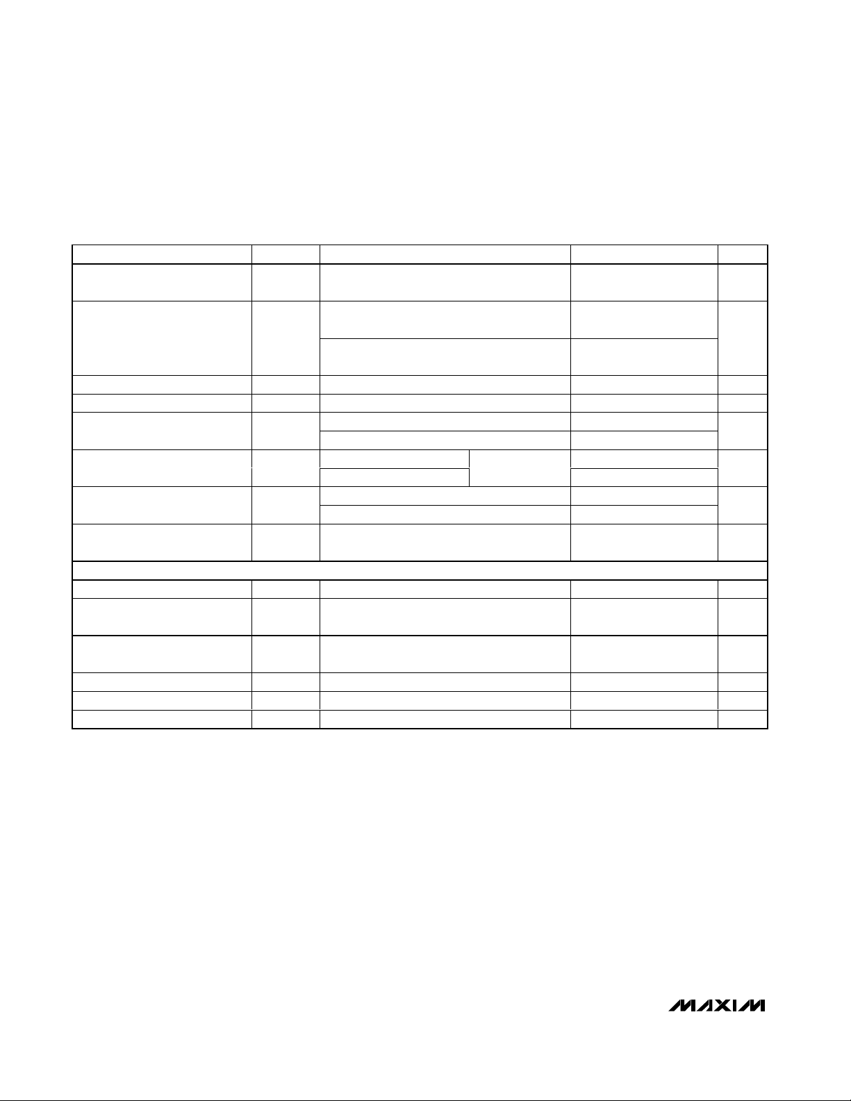
ELECTRICAL CHARACTERISTICS
(V
DCIN
= V
CSSP
= V
CSSN
= 18V, V
BATT
= V
CSIP
= V
CSIN
= 12V, V
REFIN
= 3.0V, V
VCTL
= V
ICTL
= 0.75 ✕REFIN, CELLS = 2.0V,
ACIN = 0, CLS = REF, V
BST
- VLX= 4.5V, GND = PGND = 0, C
LDO
= 1µF, LDO = DLOV, C
REF
= 1µF; pins CCI, CCS, and CCV are
compensated per Figure 1a; T
A
= -40°C to +85°C, unless otherwise noted.) (Note 1)
PARAMETER
SYMBOL
CONDITIONS
MIN TYP MAX UNITS
SUPPLY AND LDO REGULATOR
DCIN Input Voltage Range
V
DCIN
8.0
V
DCIN falling 7
DCIN Undervoltage Lockout
Trip Point
DCIN rising
V
DCIN Quiescent Current
I
DCIN
8.0V < V
DCIN
< 28V
6 mA
LDO Output Voltage
8.0V < V
DCIN
< 28V, no load
V
TRIP POINTS
BATT POWER_FAIL Threshold
V
CSSP
falling
50
mV
BATT POWER_FAIL Threshold
Hysteresis
mV
ACIN Threshold ACIN rising
V
ACIN Threshold Hysteresis 0.5% of REF 10 30 mV
ACIN Input Bias Current
V
ACIN
= 2.048V
-1 +1 µA
CLS Input Range 1.6
V
CLS Input Bias Current
V
CLS
= 2.0V
-1 +1 µA
SWITCHING REGULATOR
Minimum Off-Time
V
BATT
= 16.8V
1 1.5 µs
Maximum On-Time 5 15 ms
Oscillator Frequency
f
OSC
(Note 1)
kHz
DHI Maximum Duty Cycle 99 %
V
BATT
= 19V, V
DCIN
= 0
5
BATT Input Current
I
BATT
V
BATT
= 2V to 19V, V
DCIN
> V
BATT
+ 0.3V
µA
V
DCIN
= 0
5
CSIP/CSIN Input Current
V
CSIP
= V
CSIN
= 12V
µA
V
DCIN
= 0
0.3
CSSP/CSSN Input Current
V
CSSP
= V
CSSN
= V
DCIN
> 8.0V
µA
BATT/CSIP/CSIN Input Voltage
Range
0 19 V
CSIP to CSIN Full-Scale
Current-Sense Voltage
V
BATT
= 12V
mV
CSSP to CSSN Full-Scale
Current-Sense Voltage
mV
CURRENT AND VOLTAGE SETTING
ICTL = REFIN (see Equation 2) -8 +8
Charging Current Accuracy
ICTL = REFIN/32 (see Equation 2) -55
%
V
VCTL
= V
ICTL
= V
REFIN
= 3V
-1 +1
ICTL, VCTL, REFIN Input Bias
Current
V
DCIN
= 0, V
VCTL
= V
ICTL
= V
REFIN
= 5V
-1 +1
µA
5.25
100
2.007
189
189
28.0
7.85
5.65
150
300
2.089
REF
400
500
800
800
219
219
+55
Page 6
MAX1772
Low-Cost, Multichemistry BatteryCharger Building Block
6 _______________________________________________________________________________________
ELECTRICAL CHARACTERISTICS (continued)
(V
DCIN
= V
CSSP
= V
CSSN
= 18V, V
BATT
= V
CSIP
= V
CSIN
= 12V, V
REFIN
= 3.0V, V
VCTL
= V
ICTL
= 0.75 ✕REFIN, CELLS = 2.0V,
ACIN = 0, CLS = REF, V
BST
- VLX= 4.5V, GND = PGND = 0, C
LDO
= 1µF, LDO = DLOV, C
REF
= 1µF; pins CCI, CCS, and CCV are
compensated per Figure 1a; T
A
= -40°C to +85°C, unless otherwise noted.) (Note 1)
PARAMETER
SYMBOL
CONDITIONS
MIN TYP MAX UNITS
ICTL Power-Down Mode
Threshold Voltage
REFIN
REFIN
/33
V
V
VCTL
= V
REFIN
(2, 3, or 4 cells)
(see Equation 1)
-1 +1
Battery Regulation Voltage
Accuracy
V
VCTL
= V
REFIN
/20 (2, 3, or 4 cells)
(see Equation 1)
-1 +1
%
REFIN Range 2.0 3.6 V
REFIN Undervoltage Lockout
V
V
CSIP
- V
CSIN
= 0.185V
-5 +5
ICHG Accuracy
V
CSIP
- V
CSIN
= 0.05V
-10
%
V
CSSP
- V
CSSN
= 0.185V
-15
IINP Current Accuracy
V
CSSP
- V
CSSN
= 0.05V
(Note 2)
-20
%
V
CSSP
- V
CSSN
= 0.08V, V
CLS
= 1.6V
-10
CSSP - CSSN Accuracy
V
CSSP
- V
CSSN
= 0.2V, CLS = REF
-10
%
CSSP + CSSN Input Voltage
Range
8 28 V
LOGIC LEVELS
CELLS Input Low Voltage 0.2 V
CELLS Input Middle Voltage 0.4
V
LDO
V
CELLS Input High Voltage
V
LDO
V
CELLS Input Bias Current
CELLS = 0 or V
LDO
-10
µA
ACOK Sink Current
V
ACOK
= 0.4V
1 mA
ACOK Leakage Current
V
ACOK
= 5.5V
-1 +1 µA
Note 1: Guaranteed by design. Not production tested.
Note 2: Tested under DC conditions. See text for more detail.
/100
1.92
+10
+15
+20
+10
+10
- 0.25
- 0.5
V
LDO
+10
Page 7

MAX1772
Low-Cost, Multichemistry Battery-
Charger Building Block
_______________________________________________________________________________________ 7
Typical Operating Characteristics
(Circuit of Figure 1a, V
DCIN
= 20V, TA = +25°C, unless otherwise noted.)
V
BATT
20V/div
I
BATT
2A/div
CCI
500mV/div
CCV
500mV/div
LOAD-TRANSIENT RESPONSE
(BATTERY REMOVAL AND REINSERTION)
MAX1772 toc01
1ms/div
ICTL = 0.957V
VCTL = 3.3V
BATTERY PRESENT
CCI
CCV
V
BATT
20V/div
I
LOAD
2A/div
CCS
500mV/div
CCI
500mV/div
LOAD-TRANSIENT RESPONSE
(STEP-IN LOAD CURRENT)
MAX1772 toc02
1ms/div
ICTL = 3.30V
CHARGING CURRENT = 2.0A
V
BATT
= 16V
LOAD STEP = 0 TO 3A
I
SOURCE
LIMIT = 5A
CCI
CCS
V
BATT
(AC-COUPLED)
100mV/div
DCIN
10V/div
LINE-TRANSIENT RESPONSE
MAX1772 toc03
2ms/div
V
BATT
= 16V
DCIN = 18.5V TO 27.5V
I
LOAD
= 150mA
-0.4
-0.2
-0.3
-0.1
0.2
0.3
0.1
0
0.4
0 23451 678910
LDO LOAD REGULATION
MAX1772 toc04
LDO CURRENT (mA)
LDO ERROR (%)
VCTL = 0
ICTL = 3.3V
DCIN = 20.0V
LDO = 5.40V
Page 8

MAX1772
Low-Cost, Multichemistry BatteryCharger Building Block
8 _______________________________________________________________________________________
-0.5
-0.2
-0.3
-0.4
-0.1
0
0.1
0.2
0.3
0.4
0.5
-40 10-15 356085
REF VOLTAGE ERROR vs. TEMPERATURE
MAX1772 toc07
TEMPERATURE (°C)
REF VOLTAGE ERROR (%)
ICTL = 0
VCTL = 0
NO LOAD
REF = 4.096V
100
0
0.1 1 10 100 1000 10,000
EFFICIENCY vs. BATTERY CURRENT
(VOLTAGE CONTROL LOOP)
20
MAX1772 toc08
BATT CURRENT (mA)
EFFICIENCY (%)
40
60
80
10
30
50
70
90
VCTL = 0
ICTL = 3.3V
REFIN = 3.3V
CELL = 3
CELL = 2
CELL = 4
100
0
100 1000 10,000
EFFICIENCY vs. BATTERY CURRENT
(CURRENT CONTROL LOOP)
20
MAX1772 toc09
EFFICIENCY (%)
40
60
80
10
30
50
70
90
VCTL = 0
ICTL = 3.3V
REFIN = 3.3V
CELL = 2
CELL = 3
CELL = 4
BATT CURRENT (mA)
Typical Operating Characteristics (continued)
(Circuit of Figure 1a, V
DCIN
= 20V, TA = +25°C, unless otherwise noted.)
-1.0
-0.6
-0.8
-0.2
-0.4
0.2
0
0.4
0.8
0.6
1.0
8162012 24 28
LDO LINE REGULATION
MAX1772 toc05
DCIN (V)
LDO ERROR (%)
LDO = 5.40V
-0.20
-0.10
-0.15
-0.05
0.10
0.15
0.05
0
0.20
0 100 150 200 25050 300 350 400 450 500
REF VOLTAGE LOAD REGULATION
MAX1772 toc06
REF CURRENT (μA)
REF ERROR (%)
VCTL = 0
ICTL = 3.3V
CELL = 4
REF = 4.096V
Page 9

MAX1772
Low-Cost, Multichemistry Battery-
Charger Building Block
_______________________________________________________________________________________ 9
Typical Operating Characteristics (continued)
(Circuit of Figure 1a, V
DCIN
= 20V, TA = +25°C, unless otherwise noted.)
0
0.010
0.005
0.020
0.015
0.030
0.025
0.035
0.045
0.040
0.050
0 1000 1500500 2000 2500 3000 3500 4000
OUTPUT V/I CHARACTERISTICS
MAX1772 toc10
BATT CURRENT (mA)
BATT VOLTAGE ERROR (%)
VCTL = 0
ICTL = 3.3V
CELL = 4
CELL = 3
CELL = 2
0
0.04
0.02
0.08
0.06
0.12
0.10
0.14
0.18
0.16
0.20
0 0.2 0.3 0.40.1 0.5 0.6 0.7 0.90.8 1.0
BATT VOLTAGE ERROR vs. VCTL
MAX1772 toc11
VCTL/REFIN (%)
BATT VOLTAGE ERROR (%)
CELL = 4
REFIN = 3.3V
NO LOAD
0
1
2
4
3
5
00.40.2 0.6 0.80.1 0.50.3 0.7 0.9 1.0
CURRENT SETTING ERROR vs. ICTL
MAX1772 toc12
ICTL/REFIN (%)
CURRENT SETTING ERROR (%)
BATT > 2V
REFIN = 3.3V
0
0.5
1.5
1.0
2.5
2.0
3.5
3.0
4.0
0 1000 1500500 2000 2500 3000 3500 4000
ICHG ERROR vs. BATT LOAD CURRENT
MAX1772 toc13
BATT LOAD CURRENT (mA)
ICHG ERROR (%)
VCTL = 0
ICTL = 3.3V
CELL = 4
Page 10

MAX1772
Low-Cost, Multichemistry BatteryCharger Building Block
10 ______________________________________________________________________________________
PIN NAME FUNCTION
1 DCIN Charging Voltage Input
2 LDO D evi ce P ow er S up p l y. Outp ut of the 5.4V l i near r eg ul ator sup p l i ed fr om D C IN . Byp ass w i th a 1µF cap aci tor .
3 CLS Source Current-Limit Input. Voltage input for setting the current limit of the input source.
4 REF 4.096V Voltage Reference. Bypass with 1µF to GND.
5 CCS Input Current Regulation Loop Compensation Point. Use 0.01µF to GND.
6 CCI Output Current Regulation Loop Compensation Point. Connect 0.01µF to GND.
7 CCV Voltage Regulation Loop Compensation Point. Connect 1kΩ in series with 0.1µF to GND.
8, 9 GND Analog Ground
10 ICHG
ICHG is a scaled-down replica of the battery output current being sensed. It is used to monitor the
charging current and indicates when the chip changes from voltage mode to current mode. The
transconductance of (CSIP - CSIN) to ICHG is 1µS. Connect ICHG pin to GND if it is unused.
11 ACIN AC Detect Input. Detects when the AC adapter voltage is available for charging.
12 ACOK AC Detect Output. Open-drain output is high when ACIN is less than REF/2.
13 REFIN
Reference Input. Allows the ICTL and VCTL pins to have ratiometric ranges for increased DAC
accuracy.
14 ICTL
Input for Setting Maximum Output Current. Range is REFIN/32 to REFIN. The device shuts down if
this pin is forced below REFIN/55 (typ).
15 VCTL Input for Setting Maximum Output Voltage. Range is 0 to REFIN.
16 CELLS Trilevel Input for Setting Number of Cells. GND = 2 cells, LDO/2 = 3 cells, LDO = 4 cells.
17 BATT Battery Voltage Input
18 CSIN Output Current-Sense Negative Input
19 CSIP Output Current-Sense Positive Input. Connect a current-sense resistor from CSIP to CSIN.
20 PGND Power Ground
21 DLO Low-Side Power MOSFET Driver Output. Connect to low-side NMOS gate.
22 DLOV Low-Side Driver Supply
23 LX Power Connection for the High-Side Power MOSFET Driver. Connect to source of high-side NMOS.
24 DHI High-Side Power MOSFET Driver Output. Connect to high-side NMOS gate.
25 BST
Power Connection for the High-Side Power MOSFET Driver. Connect a 0.1µF capacitor from LX to
BST.
26 CSSN Input Current-Sense for Charger (negative input)
27 CSSP
Input Current-Sense for Charger (positive input). Connect a current-sense resistor from CSSP to
CSSN.
28 IINP
IIN P i s a scal ed - d ow n r ep l i ca of the i np ut cur r ent b ei ng sensed . It i s used to m oni tor the total system
cur r ent. The tr anscond uctance of ( C S S P - C S S N ) to IIN P i s 1m S . C onnect IIN P p i n to GN D i f i t i s unused .
Pin Description
Page 11

MAX1772
Low-Cost, Multichemistry Battery-
Charger Building Block
______________________________________________________________________________________ 11
Detailed Description
The MAX1772 includes all of the functions necessary to
charge Li+, NiMH, and NiCd batteries. A high-efficiency
synchronous-rectified step-down DC-DC converter controls charging voltage and current. It also includes input
source-current limiting and analog inputs for setting the
charge current and charge voltage. The DC-DC converter uses external N-channel MOSFETs as the buck
switch and synchronous rectifier to convert the input
voltage to the required charging current and voltage.
The typical application circuit shown in Figure 1a uses
a microcontroller (µC) to allow control of charging current or voltage, while Figure 1b shows a typical application with charging voltage and current fixed to
specific values for the application. The voltage at ICTL
and the value of RS2 set the charging current. The DCDC converter generates the control signals for the
external MOSFETs to regulate the voltage and the current set by the VCTL, ICTL, and CELLS inputs.
The MAX1772 features a voltage-regulation loop (CCV)
and two current-regulation loops (CCI and CCS). The
CCV voltage-regulation loop monitors BATT to ensure
that its voltage never exceeds the voltage set by VCTL.
The CCI battery current-regulation loop monitors current delivered to BATT to ensure that it never exceeds
the current limit set by ICTL. A third loop (CCS) takes
control and reduces the battery-charging current when
the sum of the system load and the battery-charging
current exceeds the charging source current limit set
by CLS.
Setting the Battery Regulation Voltage
The MAX1772 uses a high-accuracy voltage regulator
for charging voltage. The VCTL input adjusts the battery output voltage. VCTL is allowed to vary from 0 to
REFIN (≈ 3.3V). The per-cell battery termination voltage
is a function of the battery chemistry and construction;
thus, consult the battery manufacturer to determine this
voltage. The battery voltage is calculated by the equation:
CELLS is the programming input for selecting cell
count. Table 1 shows how CELLS is connected to
charge 2, 3, or 4 cells. Use a voltage-divider from LDO
to set the desired voltage at CELLS.
The internal error amplifier (GMV) maintains voltage
regulation (Figure 2). The voltage error amplifier is compensated at CCV. The component values shown in
Figure 1 provide suitable performance for most appli-
cations. Individual compensation of the voltage regulation and current-regulation loops allow for optimal compensation.
Setting the Charging-Current Limit
The ICTL input sets the maximum charging current. The
current is set by current-sense resistor RS2, connected
between CSIP and CSIN. The nominal differential voltage between CSIP and CSIN is 204mV; thus, for a
0.05Ω sense resistor, the maximum charging current is
4A. Battery-charging current is programmed with ICTL
using the equation:
The input range for ICTL is REFIN/32 to REFIN (≈ 3.3V).
The device shuts down if ICTL is forced below
REFIN/55 (typical). The current at ICHG is a scaleddown replica of the battery output current being sensed
across CSIP and CSIN.
When choosing the current-sense resistor, note that the
voltage drop across this resistor causes further power
loss, reducing efficiency. However, adjusting ICTL to
reduce the voltage across the current-sense resistor
may degrade accuracy due to the input offset of the
current-sense amplifier. The charging current-error
amplifier (GMI) is compensated at CCI. A 0.01µF
capacitor at CCI provides suitable performance for
most applications.
Setting the Input Current Limit
The total input current (from a wall cube or other DC
source) is a function of the system supply current and
the battery-charging current. The input current regulator limits the source current by reducing the charging
current when the input current exceeds the set input
current limit. System current will normally fluctuate as
portions of the system are powered up or put to sleep.
Without input current regulation, the input source must
be able to supply the maximum system current and the
maximum charger input current. By using the input current limiter, the current capability of the AC wall adapter
may be lowered, reducing system cost.
The MAX1772 limits the current drawn by the charger
when the load current becomes high. The device limits
the charging current, so the AC adapter voltage is not
loaded down. An internal amplifier compares the voltage between CSSP and CSSN to the voltage at CLS.
V
CLS
can be set by a resistor-divider between REF and
GND. Connect CLS to REF for maximum input current
limiting.
I
V
RS2VV
2
CHG
REF ICTL
REFIN
=× ×
()
1
20
V ELLS V
VV
V
1
BATT REF
REF VCTL
REFIN
=×+×
⎛
⎝
⎜
⎞
⎠
⎟
⎛
⎝
⎜
⎞
⎠
⎟
()
C
10
Page 12

MAX1772
Low-Cost, Multichemistry BatteryCharger Building Block
12 ______________________________________________________________________________________
Figure 1a. µC-Controlled Typical Application Circuit
DCIN
MAX1772
CLSREF
GND
CELLS
DLOV
V
IN
8VDC TO 28VDC
DHI
D3
BST
SMART
BATTERY
HOST
ACIN
D4
R6
59.0kΩ
R7
19.6kΩ
C5
1μF
VCTL
ICTL
REFIN
ACOK
ICHG
IINP
R8
1MΩ
R9
15.4kΩ
R10
12.4kΩ
C14
0.1μF
C20
0.1μF
CCV
C11
0.1μF
R5
1kΩ
CCI
CCS
C10
0.01μF
C9
0.01μF
C12
1μF
C1
22μFC222μF
C13
1μF
C15
0.1μF
LX
C16
1.0μF
LDO
R13
33Ω
CSSP CSSN
D1
C7
O.47μF
C6
O.47μF
R14
4.7Ω
R15
4.7Ω
RS1
0.04Ω
N1
L1
22μH
RS2
0.05Ω
CSIP
R11
1Ω
CSIN
R12
1Ω
PGND
DLO
N2
D2
C18
0.1μF
C19
0.1μF
BATT
C3
22μFC422μF
BATT
+
R20, R21, R22
10kΩ
AVDD/REF
SCL
SDA
TEMP
BATT-
A/D INPUT
A/D INPUT
D/A OUTPUT
D/A OUTPUT
VCC
SCL
SDA
A/D INPUT
GND
PGND GND
TO EXTERNAL
LOAD
DIGITAL
INPUT
Page 13

MAX1772
Low-Cost, Multichemistry Battery-
Charger Building Block
______________________________________________________________________________________ 13
Figure 1b. Stand-Alone Typical Application Circuit
TO EXTERNAL
LOAD
DCIN
MAX1772
CLSREF
GND
CELLS
DLOV
V
IN
8VDC TO 28VDC
DHI
D3
BST
BATTERY
ACIN
D4
R6
59.0kΩ
R7
19.6kΩ
C5
1μF
ACOK
ICHG
IINP
R8
1M
R9
15.4kΩ
R10
12.4kΩ
C14
0.1μF
C20
0.1μF
CCV
C11
0.1μF
R5
1kΩ
CCI
CCS
C10
0.01μF
C9
0.01μF
C12
1μF
C1
22μFC222μF
C13
1μF
C15
0.1μF
LX
C16
1.0μF
LDO
R13
33Ω
CSSP CSSN
D1
C7
O.47μF
C6
O.47μF
R14
4.7Ω
R15
4.7Ω
3.30V
910Ω 1.5kΩ
RS1
0.04Ω
N1
L1
22μH
RS2
0.05Ω
CSIP
R11
1Ω
CSIN
R12
1Ω
PGND
DLO
N2
D2
C18
0.1μF
C19
0.1μF
BATT
C3
22μFC422μF
BATT
+
REFIN
VCTL
BATT-
3.30V
ICTL
R19
29.4kΩ
R20
10kΩ
R21
10kΩ
R22
10kΩ
Page 14

MAX1772
Low-Cost, Multichemistry BatteryCharger Building Block
14 ______________________________________________________________________________________
Figure 2. Functional Diagram
MAX1772
DRIVER
BST
DHI
LX
LEVEL
SHIFTER
GND
GND
DRIVER
DLOV
DLO
PGND
LVC
DC-DC
CONVERTER
ICHG
LOGIC
BLOCK
REFIN
ICTL
1/55
LDO
REF
DCIN
4.096V
REFERENCE
5.4V LINEAR
REGULATOR
ACIN
ACOK
REF/2
SRDY
CCS
CLS
CSSP
CSSN
LEVEL
SHIFTER
GMS
IINP
CSIP
CSIN
ICTL
CCI
LEVEL
SHIFTER
GMI
204mV
REFIN
X ——-
VOS
CELLS
CELL SELECT
LOGIC
409mV
REFIN
X ——-
CCV
VCTL
GMV
R1
BATT
Page 15

MAX1772
Low-Cost, Multichemistry Battery-
Charger Building Block
______________________________________________________________________________________ 15
The input source current is the sum of the device current, the charger input current, and the load current.
The device current is minimal (6mA) in comparison to
the charge and load currents. The actual source current required is determined as follows:
where η is the efficiency of the DC-DC converter (85%
to 95% typ).
V
CLS
determines the reference voltage of the GMS
error amplifier. Sense resistor RS1 sets the maximum
allowable source current. Calculate the maximum current as follows:
Once the input current limit is reached, the charging
current is tapered back until the input current is below
the desired threshold.
When choosing the current-sense resistor, note that the
voltage drop across this resistor causes further power
loss, reducing efficiency.
AC Adapter Detection
Connect the AC adapter voltage through a resistive
divider to ACIN to detect when AC power is available,
as shown in Figure 1. ACOK is an open-drain output
and is high when ACIN is less than REF/2.
Current Measurement
Use ICHG to monitor the battery-charging current
being sensed across CSIP and CSIN. The output voltage range is 0 to 3V. The voltage of ICHG is proportional to the output current by the equation:
where I
CHG
is the battery-charging current, G
ICHG
is
the transconductance of ICHG (1mS typ), and R9 is the
resistor connected between ICHG and ground.
Connect ICHG pin to ground if it is not used.
Use IINP to monitor the system input current being
sensed across CSSP and CSSN. The output voltage
range is 0 to 3V. The voltage of IINP is proportional to
the output current by the equation:
where I
SOURCE
is the DC current being supplied by the
AC adapter power, G
IINP
is the transconductance of
IINP (1mS typ), and R10 is the resistor connected
between IINP and ground.
In the typical application circuit, duty cycle affects the
accuracy of V
IINP
(Figure 3). AC load current also
affects accuracy (Figure 4).
Connect IINP pin to ground if it is not used.
LDO Regulator
LDO provides a 5.4V supply derived from DCIN and
can deliver up to 15mA of current. The MOSFET drivers
are powered by DLOV and BST, which must be connected to LDO as shown in Figure 1. LDO also supplies
the 4.096V reference (REF) and most of the control circuitry. Bypass LDO with a 1µF capacitor.
DC-to-DC Converter
The MAX1772 employs a buck regulator with a bootstrapped NMOS high-side switch and a low-side NMOS
synchronous rectifier.
DC-DC Controller
The control scheme is a constant off-time variable frequency, cycle-by-cycle current mode. The off-time is
constant for a given BATT voltage. It varies with V
BATT
operation; a maximum on-time of 10ms allows the controller to achieve >99% duty cycle with continuous conduction. Figure 5 shows the controller functional
diagram.
MOSFET Drivers
The low-side driver output DLO swings from 0 to DLOV.
DLOV is usually connected through a filter to LDO. The
high-side driver output DHI is bootstrapped off LX and
swings from VLXto V
BST
. When the low-side driver
turns on, BST rises to one diode voltage below DLOV.
Filter DLOV with a resistor-capacitor (RC) circuit whose
cutoff frequency is about 50kHz. The configuration in
Figure 1 introduces a cutoff frequency of around
48kHz:
f = 1/2πRC = 1 / (2π
✕
33Ω✕0.1µF) = 48kHz (7)
V
IINP SOURCE IINP
=×××
()
IRSGR1106
V9
ICHG CHG ICHG
=×× ×
()
IRSG R25
I
SOURCE_MAX CLS
=×
()
()
VRS/20 1 4
I I I 3
SOURCE LOAD CHARGE BATT IN
=+ ×
()
×
()
[]
()
VV/ η
Table 1. Cell-Count Programming Table
CELL CELL COUNT
V
CELLS
< 0.20V 2
0.40V < V
CELLS
< V
LDO
-0.5V 3
V
LDO
- 0.25V < V
CELLS
< V
LDO
4
Page 16

MAX1772
Low-Cost, Multichemistry BatteryCharger Building Block
16 ______________________________________________________________________________________
Dropout Operation
The MAX1772 has 99.99% duty-cycle capability with a
10ms maximum on-time and 1µs off-time. This allows
the charger to achieve dropout performance limited
only by resistive losses in the DC-DC converter components (D1, N1, RS1, RS2) (Figure 1). The actual dropout
voltage is limited to 100mV between CSSP and CSIN by
the power-fail comparator.
Compensation
Each of the three regulation loops—the input current
limit, the charging current limit, and charging voltage
limit—can be compensated separately using the CCS,
CCI, and CCV pins, respectively.
The charge-current-loop error-amp output is brought
out at CCI. Likewise, the source current error-amp output is brought out at CCS; 0.01µF capacitors to ground
at CCI and CCS compensate the current loops in most
charger designs. Raising the value of these capacitors
reduces the bandwidth of these loops.
The voltage-regulating-loop error-amp output is brought
out at CCV. Compensate this loop by connecting a
series RC network from CCV to GND. Recommended
values are 1kΩ and 0.1µF. The zero set by the series
RC increases midfrequency gain to provide phase
compensation. The pole at CCV is set by the capacitor
and the voltage error-amp output impedance at low frequencies to integrate the DC error.
Component Selection
Table 2 lists the recommended components and refers
to the circuit of Figure 1. The following sections describe
how to select these components.
MOSFETs and Schottky Diodes
Schottky diode D1 provides power to the load when the
AC adapter is inserted. This diode must be able to
deliver the maximum current as set by RS1.
The N-channel MOSFETs (N1, N2) are the switching
devices for the buck controller. High-side switch N1
should have a current rating of at least 8A and have an
on-resistance (R
DS(ON)
) of 50mΩ or less. The driver for
N1 is powered by BST; its current should be less than
10mA. Select a MOSFET with a low total gate charge
(Q
GATE
) and determine the required drive current by
I
GATE
= Q
GATE
✕
f (where f is the DC-DC converter’s
400kHz maximum switching frequency).
The low-side switch (N2) should also have a current rating of at least 8A, have an R
DS(ON)
of 100mΩ or less,
and a total gate charge less than 10nC. N2 is used to
provide the starting charge to the BST capacitor (C15).
During normal operation, the current is carried by
Schottky diode D2. Choose a Schottky diode capable
of carrying the maximum charging current.
D3 is a signal-level diode, such as the 1N4148. This
diode provides the supply current to the high-side
MOSFET driver.
Inductor Selection
Inductor L1 provides power to the battery while it is
being charged. It must have a saturation current of at
least 4A plus 1/2 of the current ripple (ΔI
L
):
I
SAT
= 4A + (1/2) ΔI
L
(8)
Figure 3. IINP Accuracy vs. V
DCIN
/
V
BATT
-10
0
10
20
30
0 1.0 1.50.5 2.0 2.5 3.0 3.5 5.04.54.0
I
RS1
(A)
IINP ACCURACY (%)
V
DCIN
= 16V
V
BATT
= 8.2
V
DCIN
= 16V
V
BATT
= 12.3
V
DCIN
= 18V
V
BATT
= 16.4
Figure 4. IINP Accuracy vs. AC Load Duty Cycle
-6
-5
-4
-3
-2
-1
0
0203010 40 50 60 70 80
DUTY CYCLE (%)
IINP ACCURACY (%)
1A
FREQUENCY
2A
AC LOAD
AC ADAPTER
RS1
MAX1772
FREQ = 125kHz
FREQ = 50kHz
FREQ = 250kHz
Page 17

MAX1772
Low-Cost, Multichemistry Battery-
Charger Building Block
______________________________________________________________________________________ 17
Figure 5. DC-to-DC Converter Functional Diagram
IMAX
RESET
4.0V
0.25V
0.1V
10ms
LVC
CONTROL
CELLS
SETV
SETI
CCVCCICCS
GMS
GMI
GMV
CLS
DLO
DHI
CSI
1μs
BST
S
RQ
CCMP
ZCMP
IMIN
CHG
RQ
S
CSS
CSSP
DCIN
CSSN
BST
DHI
LX
RS1
LDO
C
BST
L1
RS2
DLO
CSIP
CSIN
C
OUT
BATT
BATTERY
MAX1772
Q
CELL
SELECT
LOGIC
Page 18

MAX1772
Low-Cost, Multichemistry BatteryCharger Building Block
18 ______________________________________________________________________________________
The controller determines the constant off-time period,
which is dependent on BATT voltage. This makes the
ripple current independent of input and battery voltage,
and it should be kept to less than 1A. Calculate ΔILwith
the following equation:
(9)
Higher inductor values decrease the ripple current.
Smaller inductor values require high saturation current
capabilities and degrade efficiency. Typically, a 22µH
inductor is ideal for all operating conditions.
Current-Sense Input Filtering
In normal circuit operation with typical components, the
current-sense signals can have high-frequency transients that exceed 0.5V due to large current changes
and parasitic component inductance. To achieve proper battery and input current compliance, the currentsense input signals should be filtered to remove large
common-mode transients. The input current-limit sensing circuitry is the most sensitive case due to large current steps in the input filter capacitors (C6, C7) in
Figure 1. Use 0.47µF ceramic capacitors from CSSP
and CSSN to ground. Smaller 0.1µF ceramic capacitors
(C18, C19) can be used on the CSIP and CSIN inputs
to ground since the current into the battery is continuous. Place these capacitors next to the single-point
ground directly under the MAX1772.
Layout and Bypassing
Bypass DCIN with a 1µF to ground (Figure 1). D4 protects the MAX1772 when the DC power source input is
reversed. A signal diode for D4 is adequate because
DCIN only powers the LDO and the internal reference.
Bypass LDO, BST, DLOV, and other pins as shown in
Figure 1.
Good PC board layout is required to achieve specified
noise, efficiency, and stable performance. The PC board
layout artist must be given explicit instructions—preferably, a pencil sketch showing the placement of the
power switching components and high current routing.
Refer to the PC board layout in the MAX1772 evaluation
kit for examples. A ground plane is essential for optimum
performance. In most applications, the circuit will be
located on a multilayer board, and full use of the four or
more copper layers is recommended. Use the top layer
for high current connections, the bottom layer for quiet
connections (REF, CCV, CCI, CCS, DCIN, and GND),
and the inner layers for an uninterrupted ground plane.
Use the following step-by-step guide:
1) Place the high power connections first, with their
grounds adjacent:
• Minimize the current-sense resistor trace
lengths, and ensure accurate current sensing
with Kelvin connections.
• Minimize ground trace lengths in the high
current paths.
• Minimize other trace lengths in the high current
paths.
• Use >5mm wide traces.
• Connect C1 and C2 to high-side MOSFET
(10mm max length).
• LX node (MOSFETs, rectifier cathode, inductor
(15mm max length)).
Ideally, surface-mount power components are flush
against one another with their ground terminals
almost touching. These high-current grounds are
then connected to each other with a wide, filled
zone of top-layer copper, so they do not go through
vias.
The resulting top-layer subground plane is connected to the normal inner-layer ground plane at the
output ground terminals, which ensures that the
IC’s analog ground is sensing at the supply’s output
terminals without interference from IR drops and
ground noise. Other high current paths should also
be minimized, but focusing primarily on short
ground and current-sense connections eliminates
about 90% of all PC board layout problems.
2) Place the IC and signal components. Keep the
main switching node (LX node) away from sensitive
analog components (current-sense traces and REF
capacitor). Important: the IC must be no further
than 10mm from the current-sense resistors.
Keep the gate drive traces (DHI, DLO, and BST)
shorter than 20mm, and route them away from the
current-sense lines and REF. Place ceramic bypass
capacitors close to the IC. The bulk capacitors can
be placed further away. Place the current-sense
input filter capacitors under the part, connected
directly to the GND pin.
3) Use a single-point star ground placed directly
below the part. Connect the input ground trace,
power ground (subground plane), and normal
ground to this node.
ΔI
Vs
LH
L
=
()
21 μ
μ
Page 19

MAX1772
Low-Cost, Multichemistry Battery-
Charger Building Block
______________________________________________________________________________________ 19
Chip Information
TRANSISTOR COUNT: 2733
PROCESS: S12
Table 2. Component List
DESIGNATION
DESCRIPTION
C1, C2, C3, C4
22µF, 35V low-ESR tantalum capacitors
AVX TPSE226M035R0300 or
Sprague 593D226X0035E2W
C5
1µF, 50V ceramic capacitor (1210)
Murata GRM42-2X7R105K050
C6, C7
0.47µF, 25V ceramic capacitors (1210)
Murata GRM42-2X7R474K050
C9, C10 0.01µF ceramic capacitors (0805)
C12, C13
1µF, 10V ceramic capacitors (0805)
Taiyo Yuden LMK212BJ105MG
C11, C14, C15,
C16, C18, C19,
C20
0.1µF, 50V ceramic capacitors (0805)
Taiyo Yuden UMK212BJ104MG or
Murata GRM40-034X7R104M050
D1
Schottky diode (DPAK)
STM-Microelectronics STPS8L30B or
ON Semiconductor MBRD630CT or
Toshiba U5FWK2C42
D2
30V, 3A Schottky diode
Nihon EC31QS03L
D3, D4
100mA Schottky diodes (SOT23)
Central Semiconductor CMPSH-3 or
Hitachi HRB0103A
L1
22µH power inductor
Sumida CDRH127-220
DESIGNATION DESCRIPTION
N-channel MOSFET
N1
N2
RS1
RS2
R5 1kΩ ±5% resistor (0805)
R6 59.0kΩ ±1% resistor (0805)
R7 19.6kΩ ±1% resistor (0805)
R8 1MΩ ±5% resistor (0805)
R9 15.4kΩ ±1% resistor (0805)
R10 12.4kΩ ±1% resistor (0805)
R11, R12 1Ω ±5% resistors (0805)
R13 33Ω ±5% resistor (1206)
R14, R15 4.7Ω ±5% resistors (1206)
R19 29.4kΩ ±1% resistor (0805)
R20, R21, R22 10kΩ ±1% resistors (0805)
International Rectifier IRF7805 or
Fairchild FDS6680
N-channel MOSFET
Fairchild FDS6612A
0.04Ω ±1%, 1W resistor
Dale WSL-2512-R040-F or
IRC LR2512-01-R040-F
0.05Ω ±1%, 1W resistor
Dale WSL-2512-R050-F or
IRC LR2512-01-R050-F
Page 20

MAX1772
Low-Cost, Multichemistry BatteryCharger Building Block
Maxim cannot assume responsibility for use of any circuitry other than circuitry entirely embodied in a Maxim product. No circuit patent licenses are
implied. Maxim reserves the right to change the circuitry and specifications without notice at any time.
20 ____________________Maxim Integrated Products, 120 San Gabriel Drive, Sunnyvale, CA 94086 408-737-7600
© 2005 Maxim Integrated Products Printed USA is a registered trademark of Maxim Integrated Products, Inc.
QSOP.EPS
E
1
1
21-0055
PACKAGE OUTLINE, QSOP .150", .025" LEAD PITCH
Package Information
(The package drawing(s) in this data sheet may not reflect the most current specifications. For the latest package outline information,
go to www.maxim-ic.com/packages.)
 Loading...