Maxim MAX1771EPA, MAX1771CPA, MAX1771C-D, MAX1771MJA, MAX1771ESA Datasheet
19-0263; Rev 1; 7/95
EVALUATION KIT MANUAL
FOLLOWS DATA SHEET
12V or Adjustable, High-Efficiency,
Low IQ, Step-Up DC-DC Controller
_______________General Description
The MAX1771 step-up switching controller provides
90% efficiency over a 30mA to 2A load. A unique current-limited pulse-frequency-modulation (PFM) control
scheme gives this device the benefits of pulse-widthmodulation (PWM) converters (high efficiency at heavy
loads), while using less than 110µA of supply current (vs.
2mA to 10mA for PWM converters).
This controller uses miniature external components. Its
high switching frequency (up to 300kHz) allows surface-mount magnetics of 5mm height and 9mm diameter. It accepts input voltages from 2V to 16.5V. The
output voltage is preset at 12V, or can be adjusted
using two resistors.
The MAX1771 optimizes efficiency at low input voltages
and reduces noise by using a single 100mV current-limit
threshold under all load conditions. A family of similar
devices, the MAX770–MAX773, trades some full-load
efficiency for greater current-limit accuracy; they provide
a 200mV current limit at full load, and switch to 100mV
for light loads.
The MAX1771 drives an external N-channel MOSFET
switch, allowing it to power loads up to 24W. If less power
is required, use the MAX756/MAX757 or MAX761/MAX762
step-up switching regulators with on-board MOSFETs.
An evaluation kit is available. Order the MAX1771EVKIT-SO.
________________________Applications
Positive LCD-Bias Generators
Flash Memory Programmers
High-Power RF Power-Amplifier Supply
Palmtops/Hand-Held Terminals
Battery-Powered Applications
Portable Communicators
____________________________Features
♦ 90% Efficiency for 30mA to 2A Load Currents
♦ Up to 24W Output Power
♦ 110µA Max Supply Current
♦ 5µA Max Shutdown Current
♦ 2V to 16.5V Input Range
♦ Preset 12V or Adjustable Output Voltage
♦ Current-Limited PFM Control Scheme
♦ Up to 300kHz Switching Frequency
♦ Evaluation Kit Available
______________Ordering Information
PART TEMP. RANGE PIN-PACKAGE
MAX1771CPA 0°C to +70°C 8 Plastic DIP
MAX1771CSA 0°C to +70°C 8 SO
MAX1771C/D 0°C to +70°C Dice*
MAX1771EPA -40°C to +85°C 8 Plastic DIP
MAX1771ESA -40°C to +85°C 8 SO
MAX1771MJA -55°C to +125°C 8 CERDIP**
* Contact factory for dice specifications.
** Contact factory for availability and processing to MIL-STD-883B.
__________________Pin Configuration
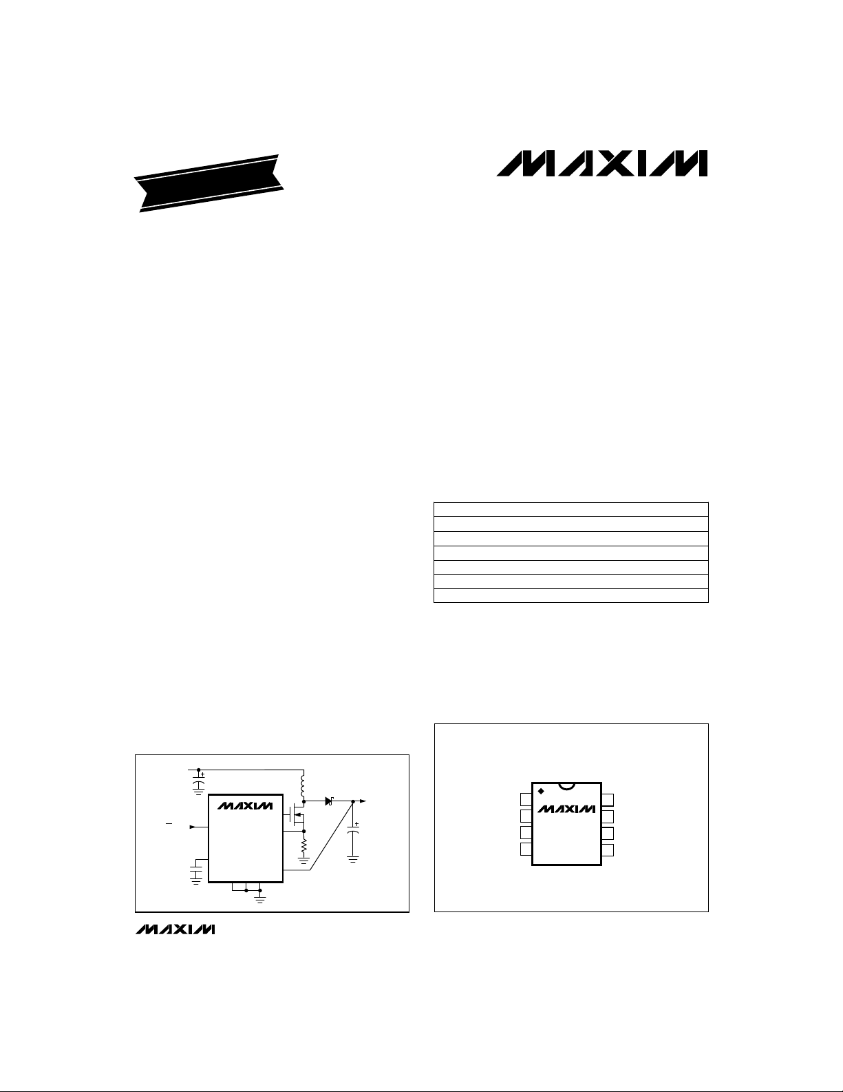
MAX1771
__________Typical Operating Circuit
TOP VIEW
INPUT
2V TO V
OUT
ON/OFF
OUTPUT
SHDN
REF
FB AGND GND
________________________________________________________________
CS
V+
N
EXT
MAX1771
12V
EXT
SHDN
1
2
V+
MAX1771
3
FB
4
DIP/SO
Maxim Integrated Products
Call toll free 1-800-998-8800 for free samples or literature.
8
CS
7
GND
6
AGND
5
REF
1
12V or Adjustable, High-Efficiency,
Low IQ, Step-Up DC-DC Controller
ABSOLUTE MAXIMUM RATINGS
Supply Voltage
V+ to GND ...............................................................-0.3V, 17V
EXT, CS, REF, SHDN, FB to GND ...................-0.3V, (V+ + 0.3V)
GND to AGND.............................................................0.1V, -0.1V
Continuous Power Dissipation (T
Plastic DIP (derate 9.09mW/°C above +70°C) ............727mW
SO (derate 5.88mW/°C above +70°C).........................471mW
CERDIP (derate 8.00mW/°C above +70°C).................640mW
= +70°C)
A
MAX1771
Stresses beyond those listed under “Absolute Maximum Ratings” may cause permanent damage to the device. These are stress ratings only, and functional
operation of the device at these or any other conditions beyond those indicated in the operational sections of the specifications is not implied. Exposure to
absolute maximum rating conditions for extended periods may affect device reliability.
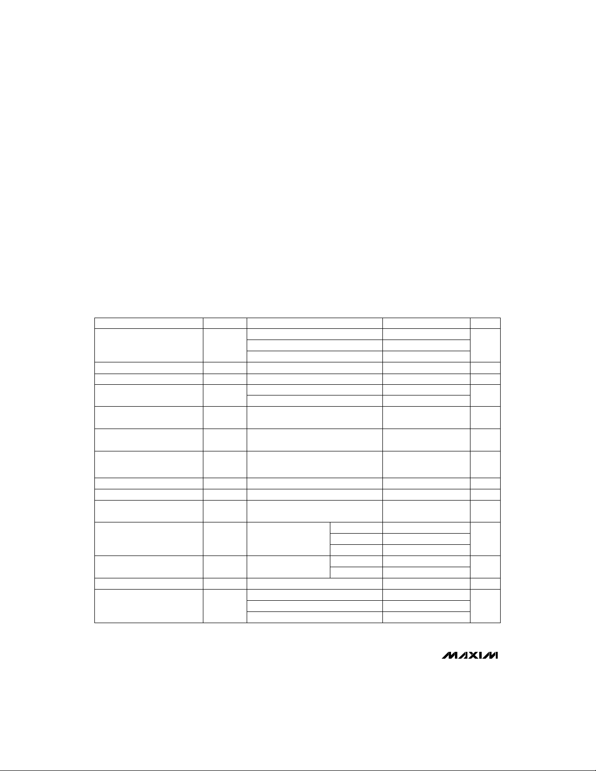
ELECTRICAL CHARACTERISTICS
(V+ = 5V, I
Input Voltage Range V
Minimum Start-Up Voltage 1.8 2.0 V
Supply Current 85 110
Standby Current
Output Voltage (Note 1) V
Output Voltage Line Regulation
(Note 2)
Output Voltage Load Regulation
(Note 2)
Maximum Switch On-Time tON(max) 12 16 20
Minimum Switch Off-Time t
Efficiency 92
Reference Voltage V
REF Load Regulation 0µA ≤ I
FB Trip Point Voltage V
= 0mA, TA= T
LOAD
PARAMETER
to T
MIN
, unless otherwise noted. Typical values are at TA= +25°C.)
MAX
SYMBOL CONDITIONS MIN TYP MAX UNITS
MAX1771 (internal feedback resistors) 2.0 12.5
MAX1771C/E (external resistors) 3.0 16.5
MAX1771MJA (external resistors) 3.1 16.5
V+ = 16.5V, SHDN = 0V (normal operation)
V+ = 10.0V, SHDN ≥ 1.6V (shutdown)
V+ = 16.5V, SHDN ≥ 1.6V (shutdown)
V+ = 2.0V to 12.0V, over full load range,
Circuit of Figure 2a
V+ = 5V to 7V, V
I
= 700mA, Circuit of Figure 2a
LOAD
V+ = 6V, V
500mA, Circuit of Figure 2a
(min) 1.8 2.3 2.8
OFF
V+ = 5V, V
Circuit of Figure 2a
I
0µA
REF
FB
REF =
REF
3V ≤ V+ ≤ 16.5V 40 100
MAX1771C 1.4700 1.5 1.5300
MAX1771E 1.4625 1.5 1.5375
MAX1771M 1.4550 1.5 1.5450
Operating Temperature Ranges
MAX1771C_A .....................................................0°C to +70°C
MAX1771E_A ..................................................-40°C to +85°C
MAX1771MJA................................................-55°C to +125°C
Junction Temperatures
MAX1771C_A/E_A.......................................................+150°C
MAX1771MJA ..............................................................+175°C
Storage Temperature Range.............................-65°C to +160°C
Lead Temperature (soldering, 10sec).............................+300°C
25
4
11.52 12.0 12.48
= 12V
= 12V, I
OUT
= 12V, I
OUT
≤ 100µA
OUT
= 0mA to
LOAD
= 500mA,
LOAD
MAX1771C 1.4700 1.5 1.5300
MAX1771E 1.4625 1.5 1.5375
MAX1771M 1.4550 1.5 1.5450
MAX1771C/E 410
MAX1771M 415
5 mV/V
20 mV/A
µA
µA
µs
µs
%
V
mV
µV/VREF Line Regulation
V
_______________________________________________________________________________________
2
12V or Adjustable, High-Efficiency,
Low IQ, Step-Up DC-DC Controller
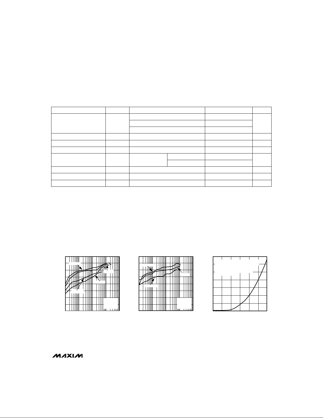
ELECTRICAL CHARACTERISTICS (continued)
(V+ = 5V, I
FB Input Current I
SHDN Input High Voltage V
SHDN Input Low Voltage V
SHDN Input Current ±1
Current-Limit Trip Level V
CS Input Current 0.01 ±1
EXT Rise Time V+ = 5V, 1nF from EXT to ground 55 ns
EXT Fall Time V+ = 5V, 1nF from EXT to ground 55 ns
Note 1: Output voltage guaranteed using preset voltages. See Figures 4a–4d for output current capability versus input voltage.
Note 2: Output voltage line and load regulation depend on external circuit components.
= 0mA, TA= T
LOAD
PARAMETERS
to T
MIN
, unless otherwise noted. Typical values are at TA= +25°C.)
MAX
SYMBOL CONDITIONS
MAX1771C ±20
FB
MAX1771M ±60
V+ = 2.0V to 16.5V 1.6 V
IH
V+ = 2.0V to 16.5V 0.4 V
IL
V+ = 16.5V, SHDN = 0V or V+
V+ = 5V to 16V
CS
MAX1771C/E
MAX1771M
MIN TYP MAX
85 100 115
75 100 125
UNITS
nAMAX1771E ±40
µA
mV
µA
__________________________________________Typical Operating Characteristics
(TA = +25°C, unless otherwise noted.)
EFFICIENCY vs. LOAD CURRENT
100
95
90
85
80
75
EFFICIENCY (%)
70
65
60
(BOOTSTRAPED MODE)
VIN = 10V
VIN = 5V
1
10
LOAD CURRENT (mA)
100
VIN = 3V
VIN = 8V
V
= 12V
OUT
CIRCUIT OF
FIGURE 2a
1000
10,000
MAX1771–01
EFFICIENCY vs. LOAD CURRENT
(NON-BOOTSTRAPED MODE)
100
95
VIN =10V
90
85
80
VIN = 5V
75
EFFICIENCY (%)
70
65
60
1
10
100
LOAD CURRENT (mA)
VIN = 8V
V
= 12V
OUT
CIRCUIT OF
FIGURE 2b
1000
10,000
700
600
MAX1771–02
500
400
300
LOAD CURRENT (mA)
200
100
0
LOAD CURRENT vs.
MINIMUM START-UP INPUT VOLTAGE
= 12V, CIRCUIT OF FIGURE 2a
V
OUT
EXTERNAL FET THRESHOLD
LIMITS FULL-LOAD START-UP
BELOW 3.5V
2.00
2.25 2.50 2.75 3.00 3.25 3.50
MINIMUM START-UP INPUT VOLTAGE (V)
MAX1771
MAX1771-TOC3
_______________________________________________________________________________________
3
12V or Adjustable, High-Efficiency,
Low IQ, Step-Up DC-DC Controller
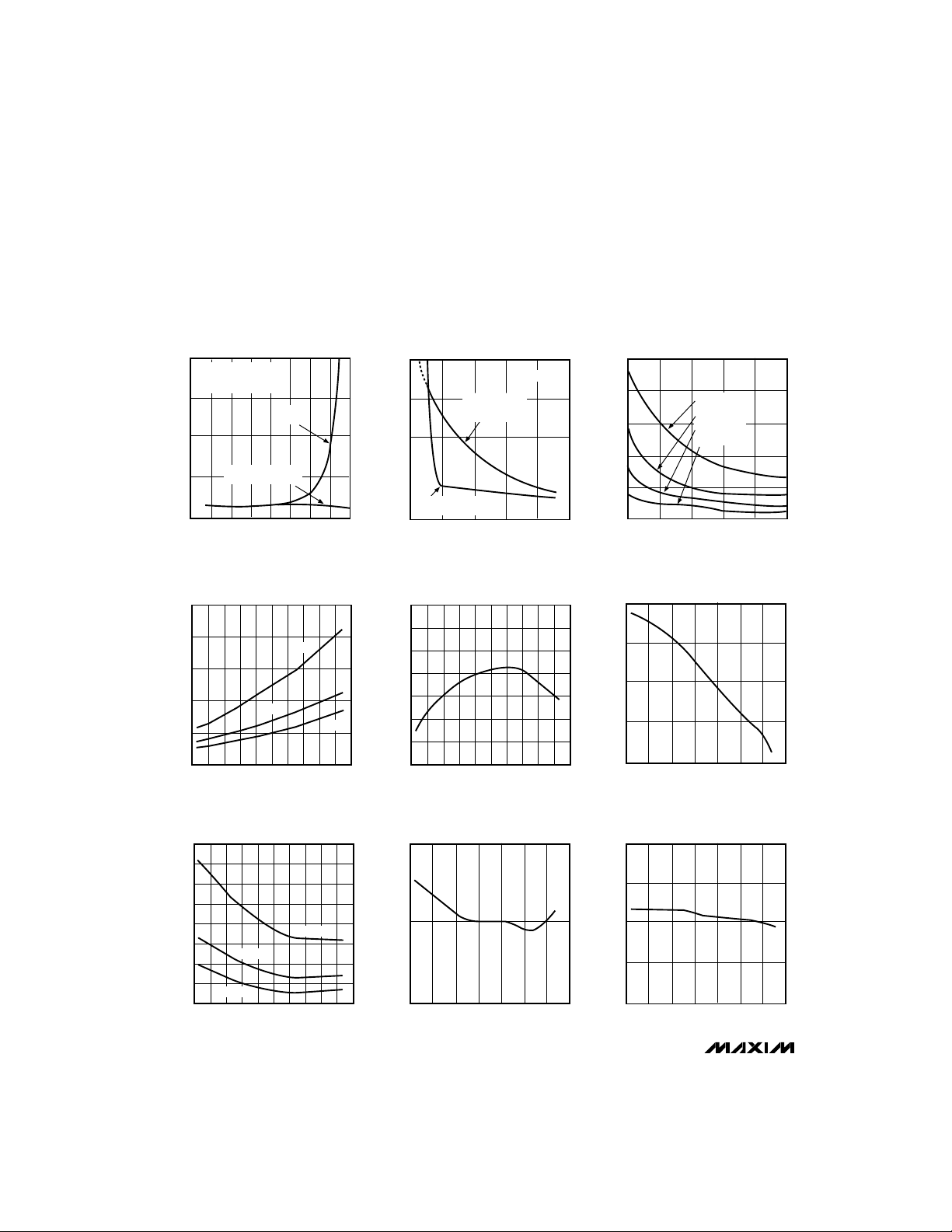
____________________________Typical Operating Characteristics (continued)
(TA = +25°C, unless otherwise noted.)
SUPPLY CURRENT vs. TEMPERATURE
4
V
= 12V, VIN = 5V
OUT
CIRCUIT OF FIGURE 2a
BOOTSTRAPPED MODE
MAX1771
3
2
SUPPLY CURRENT (mA)
250
200
150
100
50
REFERENCE OUTPUT RESISTANCE (Ω)
SCHOTTKY DIODE
1
LEAKAGE EXCLUDED
0
-50 -25 0
-75
0
-60 -20 60 140
TEMPERATURE (°C)
REFERENCE OUTPUT RESISTANCE vs.
TEMPERATURE
-40 0 8040 120
TEMPERATURE (°C)
ENTIRE
CIRCUIT
25 50 75 100 125
10µA
50µA
20 100
100µA
0.8
MAX1771-04
0.6
0.4
SUPPLY CURRENT (mA)
0.2
0
1.506
1.504
MAX1771-07
1.502
1.500
1.498
REFERENCE (V)
1.496
1.494
1.492
SUPPLY CURRENT vs. SUPPLY VOLTAGE
V
= 12V
OUT
BOOTSTRAPPED
CIRCUIT OF
FIGURE 2a
NON-BOOTSTRAPPED
CIRCUIT OF FIGURE 2b
12
2
68
4
SUPPLY VOLTAGE (V)
REFERENCE vs. TEMPERATURE
-60 -20 60 140
20 100-40 0 8040 120
TEMPERATURE (°C)
10
EXT RISE/FALL TIME vs. SUPPLY VOLTAGE
250
MAX1771-05
200
150
100
EXT RISE/FALL TIME (ns)
50
MAX1771-08
0
2
MAXIMUM SWITCH ON-TIME vs.
16.5
16.0
ON(MAX) (µs)
t
15.5
-60
68
4
SUPPLY VOLTAGE (V)
TEMPERATURE
-30 0 30 60
TEMPERATURE (°C)
C
EXT
C
EXT
C
EXT
C
EXT
= 2200pF
= 1000pF
= 446pF
= 100pF
90
10
120 150
MAX1771-06
12
MAX1771-09
SHUTDOWN CURRENT vs. TEMPERATURE
4.0
3.5
3.0
2.5
2.0
1.5
1.0
SHUTDOWN CURRENT (µA)
0.5
0
-60 -20 60 140
_______________________________________________________________________________________
4
V+ = 8V
V+ = 4V
TEMPERATURE (°C)
V+ = 15V
20 100-40 0 8040 120
MAX1771-10
MINIMUM SWITCH OFF-TIME vs.
2.30
2.25
OFF(MIN) (µs)
t
2.20
-60
TEMPERATURE
-30 0 30 60
TEMPERATURE (°C)
MAX1771-11
t
t
120 150
90
MAXIMUM SWITCH ON-TIME/
MINIMUM SWITCH OFF-TIME RATIO
8.0
7.5
7.0
OFF(MIN) RATIO
6.5
ON(MAX)/
6.0
-30 0 30 60
-60
vs. TEMPERATURE
TEMPERATURE (°C)
90
MAX1771-12
120 150
12V or Adjustable, High-Efficiency,
Low IQ, Step-Up DC-DC Controller
____________________________Typical Operating Characteristics (continued)
(Circuit of Figure 2a, TA = +25°C, unless otherwise noted.)
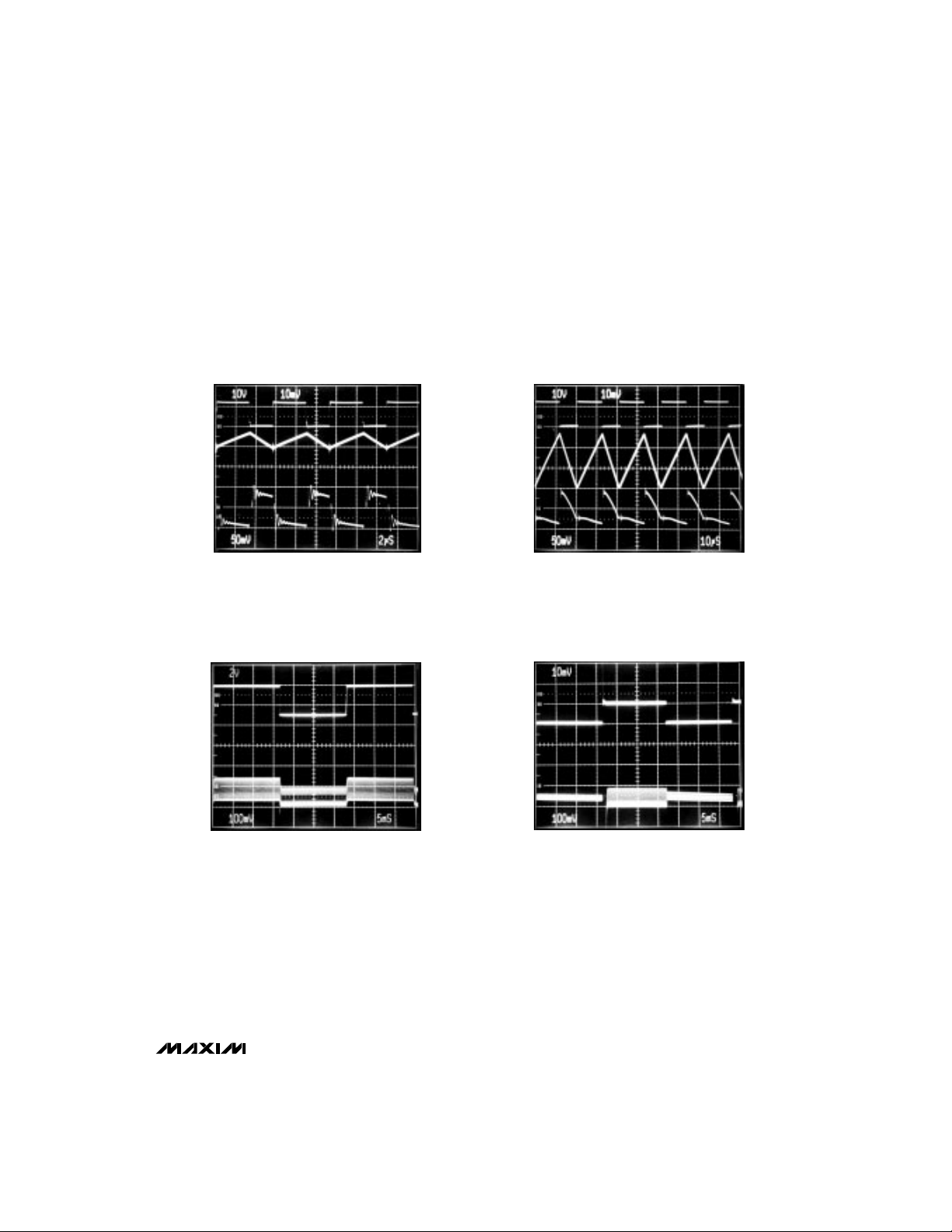
HEAVY-LOAD SWITCHING WAVEFORMS
A
B
C
= 5V, I
= 900mA, V
V
IN
OUT
A: EXT VOLTAGE, 10V/div
B: INDUCTOR CURRENT, 1A/div
RIPPLE, 50mV/div, AC-COUPLED
C: V
OUT
OUT
2µs/div
= 12V
LINE-TRANSIENT RESPONSE
A
V
OUT
0V
I
LIM
0A
7V
5V
MEDIUM-LOAD SWITCHING WAVEFORMS
A
B
C
= 5V, I
= 500mA, V
V
IN
OUT
A: EXT VOLTAGE, 10V/div
B: INDUCTOR CURRENT, 1A/div
RIPPLE, 50mV/div, AC-COUPLED
C: V
OUT
OUT
10µs/div
= 12V
LOAD-TRANSIENT RESPONSE
A
V
OUT
0V
I
LIM
0A
500mA
0A
MAX1771
B
= 700mA, V
I
OUT
, 5V to 7V, 2V/div
A: V
IN
RIPPLE, 100mV/div, AC-COUPLED
B: V
OUT
_______________________________________________________________________________________
0V
B
5ms/div
= 12V
OUT
= 6V, V
V
IN
OUT
A: LOAD CURRENT, 0mA to 500mA, 500mA/div
RIPPLE, 100mV/div, AC-COUPLED
B: V
OUT
5ms/div
= 12V
5
 Loading...