

19-0263; Rev 1; 7/95
EVALUATION KIT MANUAL
FOLLOWS DATA SHEET
12V or Adjustable, High-Efficiency,
Low IQ, Step-Up DC-DC Controller
_______________General Description
The MAX1771 step-up switching controller provides
90% efficiency over a 30mA to 2A load. A unique current-limited pulse-frequency-modulation (PFM) control
scheme gives this device the benefits of pulse-widthmodulation (PWM) converters (high efficiency at heavy
loads), while using less than 110µA of supply current (vs.
2mA to 10mA for PWM converters).
This controller uses miniature external components. Its
high switching frequency (up to 300kHz) allows surface-mount magnetics of 5mm height and 9mm diameter. It accepts input voltages from 2V to 16.5V. The
output voltage is preset at 12V, or can be adjusted
using two resistors.
The MAX1771 optimizes efficiency at low input voltages
and reduces noise by using a single 100mV current-limit
threshold under all load conditions. A family of similar
devices, the MAX770–MAX773, trades some full-load
efficiency for greater current-limit accuracy; they provide
a 200mV current limit at full load, and switch to 100mV
for light loads.
The MAX1771 drives an external N-channel MOSFET
switch, allowing it to power loads up to 24W. If less power
is required, use the MAX756/MAX757 or MAX761/MAX762
step-up switching regulators with on-board MOSFETs.
An evaluation kit is available. Order the MAX1771EVKIT-SO.
________________________Applications
Positive LCD-Bias Generators
Flash Memory Programmers
High-Power RF Power-Amplifier Supply
Palmtops/Hand-Held Terminals
Battery-Powered Applications
Portable Communicators
____________________________Features
♦ 90% Efficiency for 30mA to 2A Load Currents
♦ Up to 24W Output Power
♦ 110µA Max Supply Current
♦ 5µA Max Shutdown Current
♦ 2V to 16.5V Input Range
♦ Preset 12V or Adjustable Output Voltage
♦ Current-Limited PFM Control Scheme
♦ Up to 300kHz Switching Frequency
♦ Evaluation Kit Available
______________Ordering Information
PART TEMP. RANGE PIN-PACKAGE
MAX1771CPA 0°C to +70°C 8 Plastic DIP
MAX1771CSA 0°C to +70°C 8 SO
MAX1771C/D 0°C to +70°C Dice*
MAX1771EPA -40°C to +85°C 8 Plastic DIP
MAX1771ESA -40°C to +85°C 8 SO
MAX1771MJA -55°C to +125°C 8 CERDIP**
* Contact factory for dice specifications.
** Contact factory for availability and processing to MIL-STD-883B.
__________________Pin Configuration
MAX1771
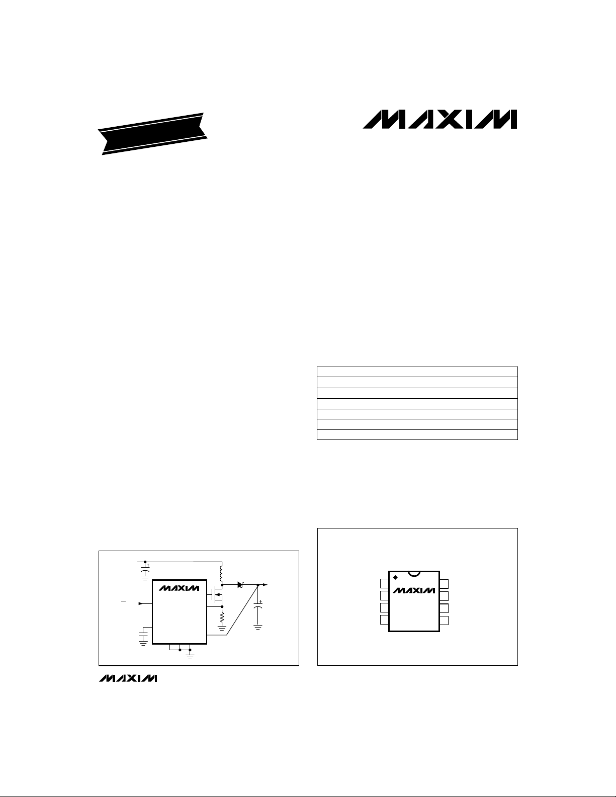
__________Typical Operating Circuit
TOP VIEW
INPUT
2V TO V
OUT
ON/OFF
OUTPUT
SHDN
REF
FB AGND GND
________________________________________________________________
CS
V+
N
EXT
MAX1771
12V
EXT
SHDN
1
2
V+
MAX1771
3
FB
4
DIP/SO
Maxim Integrated Products
Call toll free 1-800-998-8800 for free samples or literature.
8
CS
7
GND
6
AGND
5
REF
1
12V or Adjustable, High-Efficiency,
Low IQ, Step-Up DC-DC Controller
ABSOLUTE MAXIMUM RATINGS
Supply Voltage
V+ to GND ...............................................................-0.3V, 17V
EXT, CS, REF, SHDN, FB to GND ...................-0.3V, (V+ + 0.3V)
GND to AGND.............................................................0.1V, -0.1V
Continuous Power Dissipation (T
Plastic DIP (derate 9.09mW/°C above +70°C) ............727mW
SO (derate 5.88mW/°C above +70°C).........................471mW
CERDIP (derate 8.00mW/°C above +70°C).................640mW
= +70°C)
A
MAX1771
Stresses beyond those listed under “Absolute Maximum Ratings” may cause permanent damage to the device. These are stress ratings only, and functional
operation of the device at these or any other conditions beyond those indicated in the operational sections of the specifications is not implied. Exposure to
absolute maximum rating conditions for extended periods may affect device reliability.
ELECTRICAL CHARACTERISTICS
(V+ = 5V, I
Input Voltage Range V
Minimum Start-Up Voltage 1.8 2.0 V
Supply Current 85 110
Standby Current
Output Voltage (Note 1) V
Output Voltage Line Regulation
(Note 2)
Output Voltage Load Regulation
(Note 2)
Maximum Switch On-Time tON(max) 12 16 20
Minimum Switch Off-Time t
Efficiency 92
Reference Voltage V
REF Load Regulation 0µA ≤ I
FB Trip Point Voltage V
= 0mA, TA= T
LOAD
PARAMETER
to T
MIN
, unless otherwise noted. Typical values are at TA= +25°C.)
MAX
SYMBOL CONDITIONS MIN TYP MAX UNITS
MAX1771 (internal feedback resistors) 2.0 12.5
MAX1771C/E (external resistors) 3.0 16.5
MAX1771MJA (external resistors) 3.1 16.5
V+ = 16.5V, SHDN = 0V (normal operation)
V+ = 10.0V, SHDN ≥ 1.6V (shutdown)
V+ = 16.5V, SHDN ≥ 1.6V (shutdown)
V+ = 2.0V to 12.0V, over full load range,
Circuit of Figure 2a
V+ = 5V to 7V, V
I
= 700mA, Circuit of Figure 2a
LOAD
V+ = 6V, V
500mA, Circuit of Figure 2a
(min) 1.8 2.3 2.8
OFF
V+ = 5V, V
Circuit of Figure 2a
I
0µA
REF
FB
REF =
REF
3V ≤ V+ ≤ 16.5V 40 100
MAX1771C 1.4700 1.5 1.5300
MAX1771E 1.4625 1.5 1.5375
MAX1771M 1.4550 1.5 1.5450
Operating Temperature Ranges
MAX1771C_A .....................................................0°C to +70°C
MAX1771E_A ..................................................-40°C to +85°C
MAX1771MJA................................................-55°C to +125°C
Junction Temperatures
MAX1771C_A/E_A.......................................................+150°C
MAX1771MJA ..............................................................+175°C
Storage Temperature Range.............................-65°C to +160°C
Lead Temperature (soldering, 10sec).............................+300°C
25
4
11.52 12.0 12.48
= 12V
= 12V, I
OUT
= 12V, I
OUT
≤ 100µA
OUT
= 0mA to
LOAD
= 500mA,
LOAD
MAX1771C 1.4700 1.5 1.5300
MAX1771E 1.4625 1.5 1.5375
MAX1771M 1.4550 1.5 1.5450
MAX1771C/E 410
MAX1771M 415
5 mV/V
20 mV/A
µA
µA
µs
µs
%
V
mV
µV/VREF Line Regulation
V
_______________________________________________________________________________________
2
12V or Adjustable, High-Efficiency,
Low IQ, Step-Up DC-DC Controller
ELECTRICAL CHARACTERISTICS (continued)
(V+ = 5V, I
FB Input Current I
SHDN Input High Voltage V
SHDN Input Low Voltage V
SHDN Input Current ±1
Current-Limit Trip Level V
CS Input Current 0.01 ±1
EXT Rise Time V+ = 5V, 1nF from EXT to ground 55 ns
EXT Fall Time V+ = 5V, 1nF from EXT to ground 55 ns
Note 1: Output voltage guaranteed using preset voltages. See Figures 4a–4d for output current capability versus input voltage.
Note 2: Output voltage line and load regulation depend on external circuit components.
= 0mA, TA= T
LOAD
PARAMETERS
to T
MIN
, unless otherwise noted. Typical values are at TA= +25°C.)
MAX
SYMBOL CONDITIONS
MAX1771C ±20
FB
MAX1771M ±60
V+ = 2.0V to 16.5V 1.6 V
IH
V+ = 2.0V to 16.5V 0.4 V
IL
V+ = 16.5V, SHDN = 0V or V+
V+ = 5V to 16V
CS
MAX1771C/E
MAX1771M
MIN TYP MAX
85 100 115
75 100 125
UNITS
nAMAX1771E ±40
µA
mV
µA
__________________________________________Typical Operating Characteristics
(TA = +25°C, unless otherwise noted.)
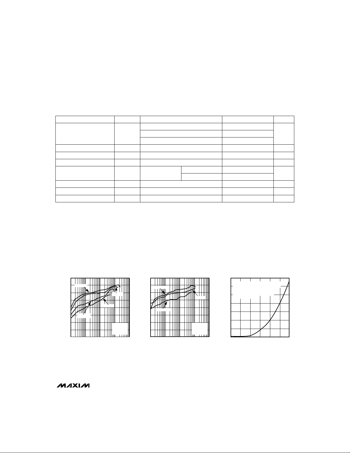
EFFICIENCY vs. LOAD CURRENT
100
95
90
85
80
75
EFFICIENCY (%)
70
65
60
(BOOTSTRAPED MODE)
VIN = 10V
VIN = 5V
1
10
LOAD CURRENT (mA)
100
VIN = 3V
VIN = 8V
V
= 12V
OUT
CIRCUIT OF
FIGURE 2a
1000
10,000
MAX1771–01
EFFICIENCY vs. LOAD CURRENT
(NON-BOOTSTRAPED MODE)
100
95
VIN =10V
90
85
80
VIN = 5V
75
EFFICIENCY (%)
70
65
60
1
10
100
LOAD CURRENT (mA)
VIN = 8V
V
= 12V
OUT
CIRCUIT OF
FIGURE 2b
1000
10,000
700
600
MAX1771–02
500
400
300
LOAD CURRENT (mA)
200
100
0
LOAD CURRENT vs.
MINIMUM START-UP INPUT VOLTAGE
= 12V, CIRCUIT OF FIGURE 2a
V
OUT
EXTERNAL FET THRESHOLD
LIMITS FULL-LOAD START-UP
BELOW 3.5V
2.00
2.25 2.50 2.75 3.00 3.25 3.50
MINIMUM START-UP INPUT VOLTAGE (V)
MAX1771
MAX1771-TOC3
_______________________________________________________________________________________
3
12V or Adjustable, High-Efficiency,
Low IQ, Step-Up DC-DC Controller
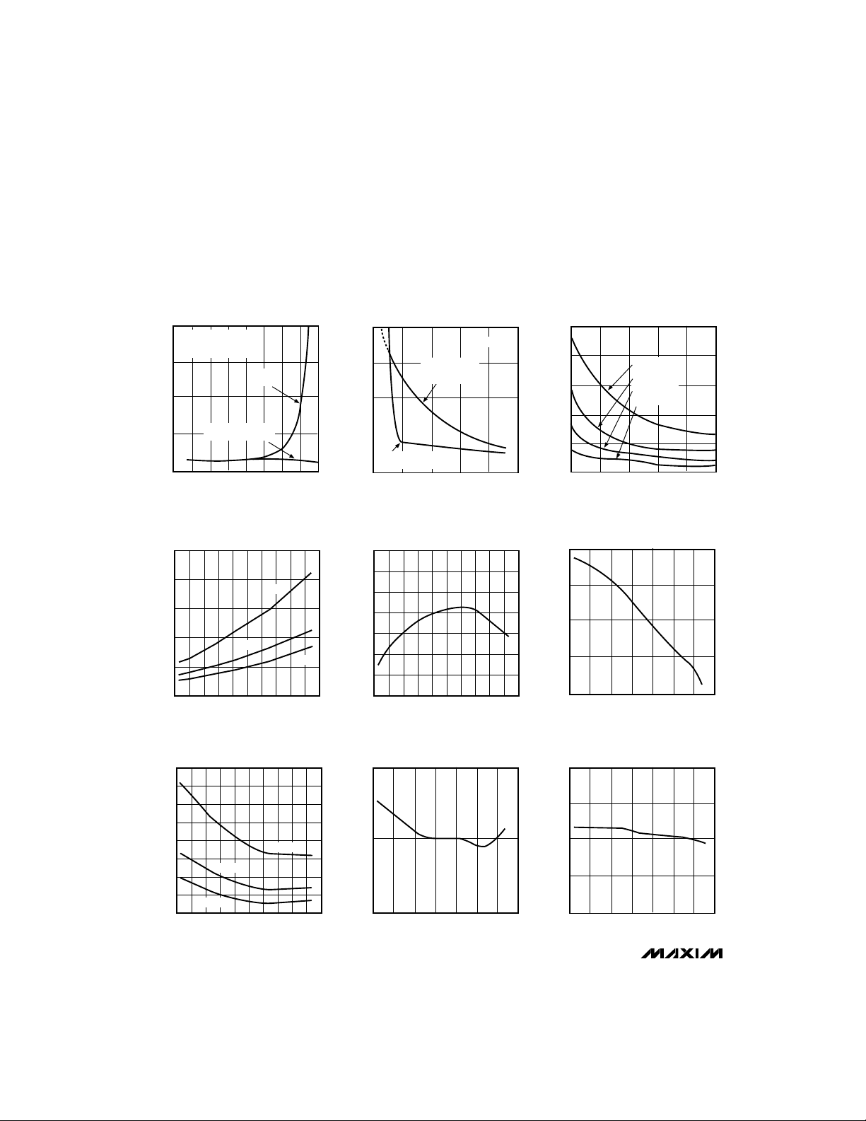
____________________________Typical Operating Characteristics (continued)
(TA = +25°C, unless otherwise noted.)
SUPPLY CURRENT vs. TEMPERATURE
4
V
= 12V, VIN = 5V
OUT
CIRCUIT OF FIGURE 2a
BOOTSTRAPPED MODE
MAX1771
3
2
SUPPLY CURRENT (mA)
250
200
150
100
50
REFERENCE OUTPUT RESISTANCE (Ω)
SCHOTTKY DIODE
1
LEAKAGE EXCLUDED
0
-50 -25 0
-75
0
-60 -20 60 140
TEMPERATURE (°C)
REFERENCE OUTPUT RESISTANCE vs.
TEMPERATURE
-40 0 8040 120
TEMPERATURE (°C)
ENTIRE
CIRCUIT
25 50 75 100 125
10µA
50µA
20 100
100µA
0.8
MAX1771-04
0.6
0.4
SUPPLY CURRENT (mA)
0.2
0
1.506
1.504
MAX1771-07
1.502
1.500
1.498
REFERENCE (V)
1.496
1.494
1.492
SUPPLY CURRENT vs. SUPPLY VOLTAGE
V
= 12V
OUT
BOOTSTRAPPED
CIRCUIT OF
FIGURE 2a
NON-BOOTSTRAPPED
CIRCUIT OF FIGURE 2b
12
2
68
4
SUPPLY VOLTAGE (V)
REFERENCE vs. TEMPERATURE
-60 -20 60 140
20 100-40 0 8040 120
TEMPERATURE (°C)
10
EXT RISE/FALL TIME vs. SUPPLY VOLTAGE
250
MAX1771-05
200
150
100
EXT RISE/FALL TIME (ns)
50
MAX1771-08
0
2
MAXIMUM SWITCH ON-TIME vs.
16.5
16.0
ON(MAX) (µs)
t
15.5
-60
68
4
SUPPLY VOLTAGE (V)
TEMPERATURE
-30 0 30 60
TEMPERATURE (°C)
C
EXT
C
EXT
C
EXT
C
EXT
= 2200pF
= 1000pF
= 446pF
= 100pF
90
10
120 150
MAX1771-06
12
MAX1771-09
SHUTDOWN CURRENT vs. TEMPERATURE
4.0
3.5
3.0
2.5
2.0
1.5
1.0
SHUTDOWN CURRENT (µA)
0.5
0
-60 -20 60 140
_______________________________________________________________________________________
4
V+ = 8V
V+ = 4V
TEMPERATURE (°C)
V+ = 15V
20 100-40 0 8040 120
MAX1771-10
MINIMUM SWITCH OFF-TIME vs.
2.30
2.25
OFF(MIN) (µs)
t
2.20
-60
TEMPERATURE
-30 0 30 60
TEMPERATURE (°C)
MAX1771-11
t
t
120 150
90
MAXIMUM SWITCH ON-TIME/
MINIMUM SWITCH OFF-TIME RATIO
8.0
7.5
7.0
OFF(MIN) RATIO
6.5
ON(MAX)/
6.0
-30 0 30 60
-60
vs. TEMPERATURE
TEMPERATURE (°C)
90
MAX1771-12
120 150
12V or Adjustable, High-Efficiency,
Low IQ, Step-Up DC-DC Controller
____________________________Typical Operating Characteristics (continued)
(Circuit of Figure 2a, TA = +25°C, unless otherwise noted.)
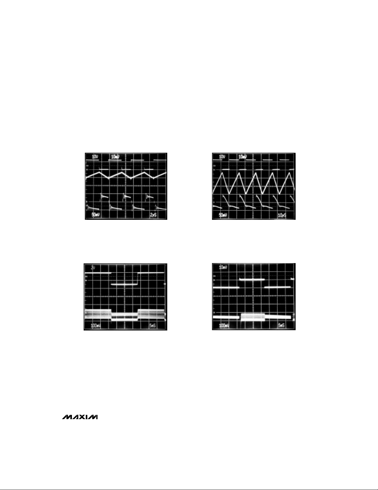
HEAVY-LOAD SWITCHING WAVEFORMS
A
B
C
= 5V, I
= 900mA, V
V
IN
OUT
A: EXT VOLTAGE, 10V/div
B: INDUCTOR CURRENT, 1A/div
RIPPLE, 50mV/div, AC-COUPLED
C: V
OUT
OUT
2µs/div
= 12V
LINE-TRANSIENT RESPONSE
A
V
OUT
0V
I
LIM
0A
7V
5V
MEDIUM-LOAD SWITCHING WAVEFORMS
A
B
C
= 5V, I
= 500mA, V
V
IN
OUT
A: EXT VOLTAGE, 10V/div
B: INDUCTOR CURRENT, 1A/div
RIPPLE, 50mV/div, AC-COUPLED
C: V
OUT
OUT
10µs/div
= 12V
LOAD-TRANSIENT RESPONSE
A
V
OUT
0V
I
LIM
0A
500mA
0A
MAX1771
B
= 700mA, V
I
OUT
, 5V to 7V, 2V/div
A: V
IN
RIPPLE, 100mV/div, AC-COUPLED
B: V
OUT
_______________________________________________________________________________________
0V
B
5ms/div
= 12V
OUT
= 6V, V
V
IN
OUT
A: LOAD CURRENT, 0mA to 500mA, 500mA/div
RIPPLE, 100mV/div, AC-COUPLED
B: V
OUT
5ms/div
= 12V
5

12V or Adjustable, High-Efficiency,
Low IQ, Step-Up DC-DC Controller
____________________________Typical Operating Characteristics (continued)
(Circuit of Figure 2a, TA = +25°C, unless otherwise noted.)
ENTERING/EXITING SHUTDOWN
MAX1771
A
0V
B
= 500mA, VIN = 5V
I
OUT
A: SHDN, 5V/div
B: V
OUT
2ms/div
, 5V/div
5V
0V
______________________________________________________________Pin Description
PIN NAME FUNCTION
1 EXT Gate Drive for External N-Channel Power Transistor
2 V+
3 FB
4 SHDN
5 REF
6 AGND Analog Ground
7 GND High-Current Ground Return for the Output Driver
8 CS
Power-Supply Input. Also acts as a voltage-sense point when in bootstrapped mode.
Feedback Input for Adjustable-Output Operation. Connect to ground for fixed-output operation.
Use a resistor divider network to adjust the output voltage. See
Active-High TTL/CMOS Logic-Level Shutdown Input. In shutdown mode, V
below V+ (due to the DC path from V+ to the output) and the supply current drops to 5µA
maximum. Connect to ground for normal operation.
1.5V Reference Output that can source 100µA for external loads. Bypass to GND with 0.1µF.
The reference is disabled in shutdown.
Positive Input to the Current-Sense Amplifier. Connect the current-sense resistor between CS
and GND.
Setting the Output Voltage
is a diode drop
OUT
section.
_______________________________________________________________________________________
6

12V or Adjustable, High-Efficiency,
Low IQ, Step-Up DC-DC Controller
_______________Detailed Description
The MAX1771 is a BiCMOS, step-up, switch-mode power-supply controller that provides a preset 12V output,
in addition to adjustable-output operation. Its unique
control scheme combines the advantages of pulse-frequency modulation (low supply current) and pulsewidth modulation (high efficiency with heavy loads),
providing high efficiency over a wide output current
range, as well as increased output current capability
over previous PFM devices. In addition, the external
sense resistor and power transistor allow the user to tailor the output current capability for each application.
Figure 1 shows the MAX1771 functional diagram.
The MAX1771 offers three main improvements over
prior pulse-skipping control solutions: 1) the converter
operates with miniature (5mm height and less than
9mm diameter) surface-mount inductors due to its
300kHz switching frequency; 2) the current-limited PFM
control scheme allows 90% efficiencies over a wide
REF
1.5V
REFERENCE
MIN OFF-TIME
ONE-SHOT
Q TRIG
2.3µs
ERROR
COMPARATOR
range of load currents; and 3) the maximum supply
current is only 110µA.
The device has a shutdown mode that reduces the
supply current to 5µA max.
Bootstrapped/Non-Bootstrapped Modes
Figure 2 shows the standard application circuits for
bootstrapped and non-bootstrapped modes. In bootstrapped mode, the IC is powered from the output
(V
, which is connected to V+) and the input voltage
OUT
range is 2V to V
. The voltage applied to the gate of
OUT
the external power transistor is switched from V
ground, providing more switch gate drive and thus
reducing the transistor’s on-resistance.
In non-bootstrapped mode, the IC is powered from the
input voltage (V+) and operates with minimum supply
current. In this mode, FB is the output voltage sense
point. Since the voltage swing applied to the gate of the
external power transistor is reduced (the gate swings
from V+ to ground), the power transistor’s on-resistance
FB
DUAL-MODE
COMPARATOR
SHDN
V+
50mV
MAX1771
N
BIAS
CIRCUITRY
OUT
MAX1771
to
MAX ON-TIME
ONE-SHOT
QTRIG
16µs
Figure 1. Functional Diagram
_______________________________________________________________________________________
F/F
QS
R
LOW-VOLTAGE
OSCILLATOR
CURRENT-SENSE
AMPLIFIER
0.1V
2.5V
EXT
CS
7

12V or Adjustable, High-Efficiency,
Low IQ, Step-Up DC-DC Controller
VIN = 5V
C2
0.1µF
5
REF
C3
0.1µF
4
MAX1771
SHDN
3
FB
6
AGND
2
V+
MAX1771
GND
7
EXT
L1
22µH
1
8
CS
C1
68µF
D1
1N5817-22
N
Si9410DY/
MTD20N03HDL
R
SENSE
40mΩ
V
OUT
C4
300µF
Figure 2a. 12V Preset Output, Bootstrapped
VIN = 4V
C2
0.1µF
5
REF
C3
0.1µF
4
SHDN
6
AGND
V
OUT
R2 = (R1) ( -1)
V
REF
V
= 1.5V
REF
2
V+
MAX1771
GND
7
EXT
22µH
1
8
CS
3
FB
L1
1N5817-22
N
Si9410DY/
MTD20N03HDL
R
SENSE
40mΩ
R1
28k
C1
47µF
D1
C4
200µF
R2
140k
C5
100pF
Figure 2c. 9V Output, Bootstrapped
increases at low input voltages. However, the supply
current is also reduced because V+ is at a lower voltage, and because less energy is consumed while
charging and discharging the external MOSFET’s gate
capacitance. The minimum input voltage is 3V when
using external feedback resistors. With supply voltages
below 5V, bootstrapped mode is recommended.
Note: When using the MAX1771 in non-bootstrapped mode, there is no preset output operation
because V+ is also the output voltage sense point
= 12V
@ 0.5A
V
OUT
= 9V
VIN = 5V
C1
68µF
C3
0.1µF
R2 = (R1) ( -1)
V
= 1.5V
REF
C2
0.1µF
2
V
V
REF
SHDN
AGND
OUT
REF
V+
MAX1771
GND
7
5
4
6
EXT
L1
22µH
1
8
CS
3
FB
D1
1N5817-22
N
MTD20N03HDL
R
SENSE
40mΩ
R1
18k
300µF
C4
R2
127k
C5
100pF
V
OUT
@ 0.5A
= 12V
Figure 2b. 12V Output, Non-Bootstrapped
for fixed-output operation. External resistors must
be used to set the output voltage. Use 1% external
feedback resistors when operating in adjustable-output
mode (Figures 2b, 2c) to achieve an overall output voltage accuracy of ±5%. To achieve highest efficiency,
operate in bootstrapped mode whenever possible.
External Power-Transistor
Control Circuitry
PFM Control Scheme
The MAX1771 uses a proprietary current-limited PFM
control scheme to provide high efficiency over a wide
range of load currents. This control scheme combines the
ultra-low supply current of PFM converters (or pulse skippers) with the high full-load efficiency of PWM converters.
Unlike traditional PFM converters, the MAX1771 uses a
sense resistor to control the peak inductor current. The
device also operates with high switching frequencies
(up to 300kHz), allowing the use of miniature external
components.
As with traditional PFM converters, the power transistor
is not turned on until the voltage comparator senses
the output is out of regulation. However, unlike traditional PFM converters, the MAX1771 switch uses the combination of a peak current limit and a pair of one-shots
that set the maximum on-time (16µs) and minimum offtime (2.3µs); there is no oscillator. Once off, the minimum off-time one-shot holds the switch off for 2.3µs.
After this minimum time, the switch either 1) stays off if
the output is in regulation, or 2) turns on again if the
output is out of regulation.
_______________________________________________________________________________________
8

12V or Adjustable, High-Efficiency,
Low IQ, Step-Up DC-DC Controller
The control circuitry allows the IC to operate in continuous-conduction mode (CCM) while maintaining high
efficiency with heavy loads. When the power switch is
turned on, it stays on until either 1) the maximum ontime one-shot turns it off (typically 16µs later), or 2) the
switch current reaches the peak current limit set by the
current-sense resistor.
The MAX1771 switching frequency is variable (depending on load current and input voltage), causing variable
switching noise. However, the subharmonic noise generated does not exceed the peak current limit times the
filter capacitor equivalent series resistance (ESR). For
example, when generating a 12V output at 500mA from
a 5V input, only 100mV of output ripple occurs using
the circuit of Figure 2a.
Low-Voltage Start-Up Oscillator
The MAX1771 features a low input voltage start-up oscillator that guarantees start-up with no load down to 2V
when operating in bootstrapped mode and using internal feedback resistors. At these low voltages, the supply
voltage is not large enough for proper error-comparator
operation and internal biasing. The start-up oscillator
has a fixed 50% duty cycle and the MAX1771 disregards the error-comparator output when the supply voltage is less than 2.5V. Above 2.5V, the error-comparator
and normal one-shot timing circuitry are used. The lowvoltage start-up circuitry is disabled if non-bootstrapped
mode is selected (FB is not tied to ground).
Shutdown Mode
When SHDN is high, the MAX1771 enters shutdown
mode. In this mode, the internal biasing circuitry is
turned off (including the reference) and V
OUT
falls to a
diode drop below VIN(due to the DC path from the
input to the output). In shutdown mode, the supply
current drops to less than 5µA. SHDN is a TTL/CMOS
logic-level input. Connect SHDN to GND for normal
operation.
__________________Design Procedure
To set the output voltage, first determine the mode of
operation, either bootstrapped or non-bootstrapped.
Bootstrapped mode provides more output current
capability, while non-bootstrapped mode reduces the
supply current (see
If a decaying voltage source (such as a battery) is
used, see the additional notes in the
Operation
section.
The MAX1771’s output voltage can be adjusted from
very high voltages down to 3V, using external resistors
Setting the Output Voltage
Typical Operating Characteristics
Low Input Voltage
FB
MAX1771
GND
Figure 3. Adjustable Output Circuit
R2
R1
C5*
R1 = 10k TO 500k
V
OUT
R2 = R1 ( -1)
V
REF
= 1.5V
V
REF
* SEE TEXT FOR VALUE
R1 and R2 configured as shown in Figure 3. For
adjustable-output operation, select feedback resistor
R1 in the 10kΩ to 500kΩ range. R2 is given by:
V
V
OUT
REF
)
where V
equals 1.5V.
REF
R2 = (R1) (––––– -1
For preset-output operation, tie FB to GND (this
forces bootstrapped-mode operation.
Figure 2 shows various circuit configurations for bootstrapped/non-bootstrapped, preset/adjustable operation.
Determining R
Use the theoretical output current curves shown in
Figures 4a–4d to select R
. They were derived
SENSE
using the minimum (worst-case) current-limit comparator threshold value over the extended temperature
range (-40°C to +85°C). No tolerance was included for
R
. The voltage drop across the diode was
SENSE
assumed to be 0.5V, and the drop across the power
switch r
and coil resistance was assumed to be
DS(ON)
0.3V.
Determining the Inductor (L)
Practical inductor values range from 10µH to 300µH.
22µH is a good choice for most applications. In applications with large input/output differentials, the IC’s
).
output current capability will be much less when the
inductance value is too low, because the IC will always
operate in discontinuous mode. If the inductor value
is too low, the current will ramp up to a high level before
the current-limit comparator can turn off the switch.
The minimum on-time for the switch (tON(min)) is
V
OUT
SENSE
MAX1771
_______________________________________________________________________________________
9

12V or Adjustable, High-Efficiency,
Low IQ, Step-Up DC-DC Controller
3.5
V
= 5V
OUT
L = 22µH
3.0
R
= 20mΩ
SENSE
2.5
R
= 25mΩ
SENSE
2.0
MAX1771
1.5
1.0
MAXIMUM OUTPUT CURRENT (A)
0.5
0
2345
R
SENSE
R
SENSE
INPUT VOLTAGE (V)
R
SENSE
= 35mΩ
= 50mΩ
= 100mΩ
Figure 4a. Maximum Output Current vs. Input Voltage
= 5V)
(V
OUT
3.5
V
= 15V
OUT
L = 22µH
3.0
R
= 20mΩ
SENSE
R
2.5
2.0
1.5
1.0
MAXIMUM OUTPUT CURRENT (A)
0.5
0
Figure 4c. Maximum Output Current vs. Input Voltage
= 15V)
(V
OUT
= 25mΩ
SENSE
R
= 35mΩ
SENSE
R
= 50mΩ
SENSE
R
= 100mΩ
SENSE
2 4 6 8 10 12 14 16
INPUT VOLTAGE (V)
approximately 2µs; select an inductor that allows the current to ramp up to I
LIM
.
The standard operating circuits use a 22µH inductor.
If a different inductance value is desired, select L such
that:
VIN(max) x 2µs
L ≥ —————----—--
I
LIM
Larger inductance values tend to increase the start-up
time slightly, while smaller inductance values allow the
coil current to ramp up to higher levels before the
switch turns off, increasing the ripple at light loads.
3.5
V
= 12V
OUT
L = 22µH
3.0
R
= 20mΩ
SENSE
R
2.5
2.0
1.5
1.0
MAXIMUM OUTPUT CURRENT (A)
0.5
0
= 25mΩ
SENSE
R
= 35mΩ
SENSE
R
= 50mΩ
SENSE
R
= 100mΩ
SENSE
2 4 6 8 10 12
INPUT VOLTAGE (V)
Figure 4b. Maximum Output Current vs. Input Voltage
(V
= 12V)
OUT
0.8
V
= 24V
OUT
L =150µH
0.6
R
= 50mΩ
SENSE
0.4
0.2
MAXIMUM OUTPUT CURRENT (A)
0
2
61014
INPUT VOLTAGE (V)
R
R
SENSE
SENSE
= 100mΩ
= 200mΩ
Figure 4d. Maximum Output Current vs. Input Voltage
= 24V)
(V
OUT
Inductors with a ferrite core or equivalent are recommended; powder iron cores are not recommended for
use with high switching frequencies. Make sure the
inductor’s saturation current rating (the current at which
the core begins to saturate and the inductance starts to
fall) exceeds the peak current rating set by R
SENSE
However, it is generally acceptable to bias the inductor
into saturation by approximately 20% (the point where
the inductance is 20% below the nominal value). For
highest efficiency, use a coil with low DC resistance,
preferably under 20mΩ. To minimize radiated noise,
use a toroid, a pot core, or a shielded coil.
Table 1 lists inductor suppliers and specific recommended inductors.
.
______________________________________________________________________________________
10

12V or Adjustable, High-Efficiency,
Low IQ, Step-Up DC-DC Controller
Use an N-channel MOSFET power transistor with the
Power Transistor Selection
MAX1771.
To ensure the external N-channel MOSFET (N-FET) is
turned on hard, use logic-level or low-threshold
N-FETs when the input drive voltage is less than 8V. This
applies even in bootstrapped mode, to ensure start-up.
N-FETs provide the highest efficiency because they do
not draw any DC gate-drive current.
When selecting an N-FET, three important parameters
are the total gate charge (Qg), on-resistance (r
and reverse transfer capacitance (C
Qgtakes into account all capacitances associated with
charging the gate. Use the typical Qgvalue for best
results; the maximum value is usually grossly overspecified since it is a guaranteed limit and not the measured value. The typical total gate charge should be
50nC or less. With larger numbers, the EXT pins may
not be able to adequately drive the gate. The EXT
rise/fall time varies with different capacitive loads as
shown in the
The two most significant losses contributing to the
N-FET’s power dissipation are I2R losses and switching
losses. Select a transistor with low r
C
RSS
Determine the maximum required gate-drive current
from the Qgspecification in the N-FET data sheet.
The MAX1771’s maximum allowed switching frequency
during normal operation is 300kHz; but at start-up, the
maximum frequency can be 500kHz, so the maximum
current required to charge the N-FET’s gate is
f(max) x Qg(typ). Use the typical Qgnumber from the
transistor data sheet. For example, the Si9410DY has a
Qg(typ) of 17nC (at VGS= 5V), therefore the current
required to charge the gate is:
The bypass capacitor on V+ (C2) must instantaneously
furnish the gate charge without excessive droop (e.g.,
less than 200mV):
Continuing with the example, ∆V+ = 17nC/0.1µF = 170mV.
Figure 2a’s application circuit uses an 8-pin Si9410DY
surface-mount N-FET that has 50mΩ on-resistance with
4.5V VGS, and a guaranteed VTHof less than 3V. Figure
2b’s application circuit uses an MTD20N03HDL logiclevel N-FET with a guaranteed threshold voltage (VTH)
of 2V.
Typical Operating Characteristics
to minimize these losses.
I
GATE
= (500kHz) (17nC) = 8.5mA.
(max)
Q
∆V+ = ——
C2
g
RSS
).
DS(ON)
DS(ON)
.
and low
),
The MAX1771’s high switching frequency demands a
high-speed rectifier. Schottky diodes such as the
1N5817–1N5822 are recommended. Make sure the
Schottky diode’s average current rating exceeds the
peak current limit set by R
down voltage exceeds V
applications, Schottky diodes may be inadequate due
to their high leakage currents; high-speed silicon
diodes such as the MUR105 or EC11FS1 can be used
instead. At heavy loads and high temperatures, the
benefits of a Schottky diode’s low forward voltage may
outweigh the disadvantages of its high leakage current.
, and that its break-
SENSE
. For high-temperature
OUT
Capacitor Selection
Output Filter Capacitor
Diode Selection
The primary criterion for selecting the output filter capacitor (C4) is low effective series resistance (ESR). The
product of the peak inductor current and the output filter
capacitor’s ESR determines the amplitude of the ripple
seen on the output voltage. Two OS-CON 150µF, 16V
output filter capacitors in parallel with 35mΩ of ESR each
typically provide 75mV ripple when stepping up from 5V
to 12V at 500mA (Figure 2a). Smaller-value and/or higher-ESR capacitors are acceptable for light loads or in
applications that can tolerate higher output ripple.
Since the output filter capacitor’s ESR affects efficiency, use low-ESR capacitors for best performance. See
Table 1 for component selection.
Input Bypass Capacitors
The input bypass capacitor (C1) reduces peak currents
drawn from the voltage source and also reduces noise
at the voltage source caused by the switching action of
the MAX1771. The input voltage source impedance
determines the size of the capacitor required at the V+
input. As with the output filter capacitor, a low-ESR
capacitor is recommended. For output currents up to
1A, 68µF (C1) is adequate, although smaller bypass
capacitors may also be acceptable.
Bypass the IC with a 0.1µF ceramic capacitor (C2)
placed as close to the V+ and GND pins as possible.
Reference Capacitor
Bypass REF with a 0.1µF capacitor (C3). REF can
source up to 100µA of current for external loads.
Feed-Forward Capacitor
In adjustable output voltage and non-bootstrapped
modes, parallel a 47pF to 220pF capacitor across R2,
as shown in Figures 2 and 3. Choose the lowest capacitor value that insures stability; high capacitance values
may degrade line regulation.
MAX1771
______________________________________________________________________________________
11

12V or Adjustable, High-Efficiency,
Low IQ, Step-Up DC-DC Controller
Table 1. Component Suppliers
PRODUCTION INDUCTORS CAPACITORS TRANSISTORS
Sumida
CD54 series
CDR125 series
Surface Mount
MAX1771
Through Hole
SUPPLIER PHONE FAX
AVX USA: (803) 448-9411 (803) 448-1943
Central
Semiconductor
Coilcraft USA: (708) 639-6400 (708) 639-1469
Coiltronics USA: (407) 241-7876 (407) 241-9339
Matsuo
Motorola USA: (800) 521-6274 (602) 952-4190
Nichicon USA: (708) 843-7500 (708) 843-2798
Nihon USA: (805) 867-2555 (805) 867-2556
Sanyo
Siliconix USA: (800) 554-5565 (408) 970-3950
Sprague USA: (603) 224-1961 (603) 224-1430
Sumida
Coiltronics
CTX20 series
Coilcraft
DO3316 series
DO3340 series
Sumida
RCH855 series
RCH110 series
USA: (516) 435-1110 (516) 435-1824
USA: (714) 969-2491 (714) 960-6492
Japan: 81-6-337-6450 81-6-337-6456
USA: (619) 661-6835 (619) 661-1055
Japan: 81-7-2070-1005 81-7-2070-1174
USA: (708) 956-0666 (708) 956-0702
Japan: 81-3-3607-5111 81-3-3607-5144
Matsuo
267 series
Sprague
595D series
AVX
TPS series
Sanyo
OS-CON series
Nichicon
PL series
Siliconix
Si9410DY
Si9420DY (high voltage)
Motorola
MTP3055EL
MTD20N03HDL
MMFT3055ELT1
MTD6N1O
MMBT8099LT1
MMBT8599LT1
DIODES
Central Semiconductor
CMPSH-3
CMPZ5240
Nihon
EC11 FS1 series (highspeed silicon)
Motorola
MBRS1100T3
MMBZ5240BL
Motorola
1N5817–1N5822
MUR115 (high voltage)
MUR105 (high-speed
silicon)
______________________________________________________________________________________
12

12V or Adjustable, High-Efficiency,
Low IQ, Step-Up DC-DC Controller
C1
2.2µF
2
MAX1771
AGND
7
R2
V+
EXT
CS
FB
6
3
†
4
3V = OFF
Figure 5. Step-Up/Down for a 5V/3.3V Output
SHDN
5
C4
REF
0.1µF
GND
SEE TEXT FOR FURTHER COMPONENT INFO
VIN MAY BE LOWER THAN INDICATED IF THE SUPPLY IS NOT
**
REQUIRED TO START UNDER FULL LOAD
**
**MOTOROLA MMFT3055ELT1
†
FOR 5V: R2 = 200kΩ, R3 = 470kΩ
3.3V: R2 = 100kΩ, R3 = 20kΩ
1
8
D2
1N5817
R3
C5
47pF
3V TO 11V
†
V
IN
Q1**
*
L1
20µH
1 CTX20-4
47µF
R1
0.1Ω
16V
V
OUT
D1
5V
1N5817
500mA
C2
L2
C3
220µF
10V
__________Applications Information
When using a power supply that decays with time
(such as a battery), the N-FET transistor will operate in
its linear region when the voltage at EXT approaches
the threshold voltage of the FET, dissipating excessive
power. Prolonged operation in this mode may damage
the FET. This effect is much more significant in nonbootstrapped mode than in bootstrapped mode, since
bootstrapped mode typically provides much higher
VGSvoltages. To avoid this condition, make sure V
is above the VTHof the FET, or use a voltage detector
(such as the MAX8211) to put the IC in shutdown mode
once the input supply voltage falls below a predetermined minimum value. Excessive loads with low input
voltages can also cause this condition.
The
Typical Operating Characteristics
Up Voltage vs. Load Current graph for bootstrappedmode operation. This graph depends on the type
of power switch used. The MAX1771 is not designed to
start up under full load in bootstrapped mode with low
input voltages.
Low Input Voltage Operation
EXT
Starting Up Under Load
show the Start-
Due to high current levels and fast switching wave-
Layout Considerations
forms, which radiate noise, proper PC board layout is
essential. Protect sensitive analog grounds by using a
star ground configuration. Minimize ground noise by
connecting GND, the input bypass capacitor ground
lead, and the output filter capacitor ground lead to a
single point (star ground configuration). Also, minimize
lead lengths to reduce stray capacitance, trace resistance, and radiated noise. Place input bypass capacitor C2 as close as possible to V+ and GND.
Excessive noise at the V+ input may falsely trigger the
timing circuitry, resulting in short pulses at EXT. If this
occurs it will have a negligible effect on circuit efficiency. If desired, place a 4.7µF directly across the V+ and
GND pins (in parallel with the 0.1µF C2 bypass capacitor) to reduce the noise at V+.
Other Application Circuits
4 Cells to 5V (or 3 Cells to 3.3V), 500mA
Step-Up/Down Converter
The circuit shown in Figure 5 generates 5V (or 3.3V) at
500mA with 85% efficiency, from an input voltage that
varies above and below the output. The output couples
to the switching circuitry via a capacitor. This configuration offers two advantages over flyback-transformer
and step-up linear-regulator circuits: smooth regulation
as the input passes through the output, and no output
current in shutdown.
This circuit requires two inductors, which can be wound
on one core with no regard to coupling since they do
not work as a transformer. L1 and L2 can either be
wound together (as with the Coiltronics CTX20-4) or
kept as two separate inductors; both methods provide
equal performance. Capacitors C2 and C3 should be
low-ESR types for best efficiency. A 1µF ceramic
capacitor will work at C2, but with about 3% efficiency
loss. C2’s voltage rating must be greater than the maximum input voltage. Also note that the LX switch must
withstand a voltage equal to the sum of the input and
output voltage; for example, when converting 11V to
5V, the switch must withstand 16V.
LX switch pulses are captured by Schottky diode D2 to
boost V+ to (V
+ VIN). This improves efficiency with
OUT
a low input voltage, but also limits the maximum input
supply to 11V. If the input voltage does not fall below 4V
and if a 3V logic threshold FET is used for Q1, you may
omit D2 and connect V+ directly to the input supply.
12V Output Buck/Boost
The circuit in Figure 6 generates 12V from a 4.5V to
16V input. Higher input voltages are possible if you
MAX1771
______________________________________________________________________________________
13

12V or Adjustable, High-Efficiency,
Low IQ, Step-Up DC-DC Controller
tries to use internal feedback and looks to V+ for its
V
IN
4.5V TO 15V
C1
OFF
4
ON
MAX1771
5
C5
0.1µF
NOTE: KEEP ALL TRACES CONNECTED
TO PIN 3 AS SHORT AS POSSIBLE
SHDN
REF
V+
MAX1771
R3
28k
1%
2
33µF
16V
EXT
AGND
GND
FB
CS
3
D2*
1N4148
L1†
20µH
D1
C2*
1µF
1N5819
1
Q1**
8
6
7
L2*
20µH
R1
0.1Ω
R2
200k
1%
*SEE TEXT FOR FURTHER
COMPONENT INFORMATION
**Q1 = MOTOROLA MMFT3055ELT1
†
L1 + L2 = ONE COILTRONICS CTX20-4
C4
C3
100µF
100µF
16V
16V
NOTE: HIGH-
CURRENT GND
Figure 6. 12V Buck/Boost from a 4.5V to 15V Input
carefully observe the component voltage ratings, since
some components must withstand the sum of the input
and output voltage (27V in this case). The circuit operates as an AC-coupled boost converter, and does not
change operating modes when crossing from buck to
boost. There is no instability around a 12V input.
Efficiency ranges from 85% at medium loads to about
82% at full load. Also, when shutdown is activated
(SHDN high) the output goes to 0V and sources no current. A 1µF ceramic capacitor is used for C2. A larger
capacitor value improves efficiency by about 1% to 3%.
D2 ensures start-up for this AC-coupled configuration
by overriding the MAX1771’s Dual-Mode feature, which
allows the use of preset internal or user-set external
feedback. When operating in Dual-Mode, the IC first
V
OUT
12V
250mA
feedback signal. However, since V+ may be greater
than the internally set feedback (12V for the MAX1771),
the IC may think the output is sufficiently high and not
start. D2 ensures start-up by pulling FB above ground
and forcing the external feedback mode. In a normal
(not AC-coupled) boost circuit, D2 isn’t needed, since
the output and FB rise as soon as input power is
applied.
Transformerless -48V to +5V at 300mA
The circuit in Figure 7 uses a transformerless design to
supply 5V at 300mA from a -30V to -75V input supply.
The MAX1771 is biased such that its ground connections are made to the -48V input. The IC’s supply voltage (at V+) is set to about 9.4V (with respect to -48V)
by a zener-biased emitter follower (Q2). An N-channel
FET (Q1) is driven in a boost configuration. Output regulation is achieved by a transistor (Q3), which level
shifts a feedback signal from the 5V output to the IC’s
FB input. Conversion efficiency is typically 82%.
When selecting components, be sure that D1, Q1, Q2,
Q3, and C6 are rated for the full input voltage plus a
reasonable safety margin. Also, if D1 is substituted, it
should be a fast-recovery type with a trrless than 30ns.
R7, R9, C8, and D3 are optional and may be used to
soft start the circuit to prevent excessive current surges
at power-up.
The circuit in Figure 8 boosts two cells (2V min) to 24V
for LCD bias or other positive output applications.
Output power is boosted from the battery input, while
V+ voltage for the MAX1771 is supplied by a 5V or 3.3V
logic supply.
The circuit in Figure 9 boosts a 2.7V to 5.5V input to a
regulated 5V, 1A output for logic, RF power, or PCMCIA
applications. Efficiency vs. load current is shown in the
adjacent graph.
Battery-Powered LCD Bias Supply
5V, 1A Boost Converter
______________________________________________________________________________________
14

12V or Adjustable, High-Efficiency,
Low IQ, Step-Up DC-DC Controller
L1
D03340
220µH–680µH
10µF
100V
EXT
AGND
C6
1
2
8
CS
2
V+
-48V
6
0.1µF
4
SHDN
C5
5
REF
3
MAX1771
FB
7
GND
Figure 7. -48V Input to 5V Output at 300mA, Without a Transformer
MBRS1100T3
3
Q1
MTD6N10
1
Q2
MMBT8099LT1
R1
0.15Ω
D1
5.1k
C8
R9
1µF
R6
R5
200k
1k
D3
CMPSH-3
R7
200Ω
2.2µF
20V
D2
CMPZ5240/
MMBZ5240BL
C4
C7
220pF
Q3
MMBT8599LT1
R2
47k
1%
R4
100k
R3
16k
1%
C1
220µF
10V
C2
220µF
10V
+5V
300mA
C3
0.33µF
MAX1771
BATTERY
INPUT
2V TO 12V
3.3V OR 5V
LOGIC
SUPPLY
ON
OFF
0.1µF
Figure 8. 2V Input to 24V Output LCD Bias
______________________________________________________________________________________
4
0.1µF
SHDN
MAX1771
L1
22µH
SENSE
0.2Ω
1N5817
N
MMFT3055ELT1
2
V+
1
EXTL
8
CS
R
3
FB
GNDREF
5
6, 7
Adj. = 12V TO 24V
(AS SHOWN)
R2
150k
R3
10k
10k
OUTPUT
47µF
15

12V or Adjustable, High-Efficiency,
Low IQ, Step-Up DC-DC Controller
INPUT
2.7V TO 5.5V
150µF
4
SHDN
ON
OFF
0.1µF
5
REF
MAX1771
Figure 9. 5V/1A Boost Converter
22µH
MAX1771
AGND
GND
76
EXT
CS
V+
FB
1
8
2
0.1µF
3
1N5820
MTD20N03HDL
0.04Ω
232k
100k
OUTPUT
100pF
5V
1A
330µF
EFFICIENCY vs. LOAD CURRENT
100
90
VIN = 4V
80
70
EFFICIENCY (%)
60
50
1m 10m 100m 1
VIN = 3V
LOAD CURRENT (A)
___________________Chip Topography
EXT
V+
CS
FB
SHDN REF
0.080"
(2.032mm)
TRANSISTOR COUNT: 501
SUBSTRATE CONNECTED TO V+
______________________________________________________________________________________
16
0.126"
(3.200mm)
GND
AGND
 Loading...