

Page 1
E V A L U A T I O N K IT A V A I L A B L E
19-5872; Rev 1; 7/11
MAX17710
Energy-Harvesting Charger and Protector
General Description
The MAX17710 is a complete system for charging and
protecting micropower-storage cells such as Infinite Power
Solution’s THINERGY® microenergy cells (MECs). The IC
can manage poorly regulated sources such as energyharvesting devices with output levels ranging from 1FW to
100mW. The device also includes a boost regulator circuit
for charging the cell from a source as low as 0.75V (typ).
An internal regulator protects the cell from overcharging.
Output voltages supplied to the target applications are
regulated using a low-dropout (LDO) linear regulator with
selectable voltages of 3.3V, 2.3V, or 1.8V. The output regulator operates in a selectable low-power or ultra-low-power
mode to minimize drain of the cell. Internal voltage protection prevents the cell from overdischarging.
The device is available in an ultra-thin, 3mm x 3mm x
0.5mm 12-pin UTDFN package.
Applications
Powered/Smart Cards
Remote Wireless
Sensors
Memory and Real-Time
Clock Backup
Semiactive RFID Tags
Medical Devices
High-Temperature
Applications
Military/DoD and
Aerospace
Toys
Features
S Integrated Power-Management IC for Energy
Storage and Load Management
S Lithium Charger
1nA Standby I
625nA Linear Charging
QBATT
1µW Boost Charging
S Lithium Cell Undervoltage Protection
S Charger Overvoltage Shunt Protection
S 1.8V, 2.3V, or 3.3V LDO (150nA I
QBATT
)
S Lithium Cell Output Buffering
S Ultra-Thin, 3mm x 3mm x 0.5mm UTDFN Package
Ordering Information appears at end of data sheet.
For related parts and recommended products to use with this part,
refer to: www.maxim-ic.com/MAX17710.related
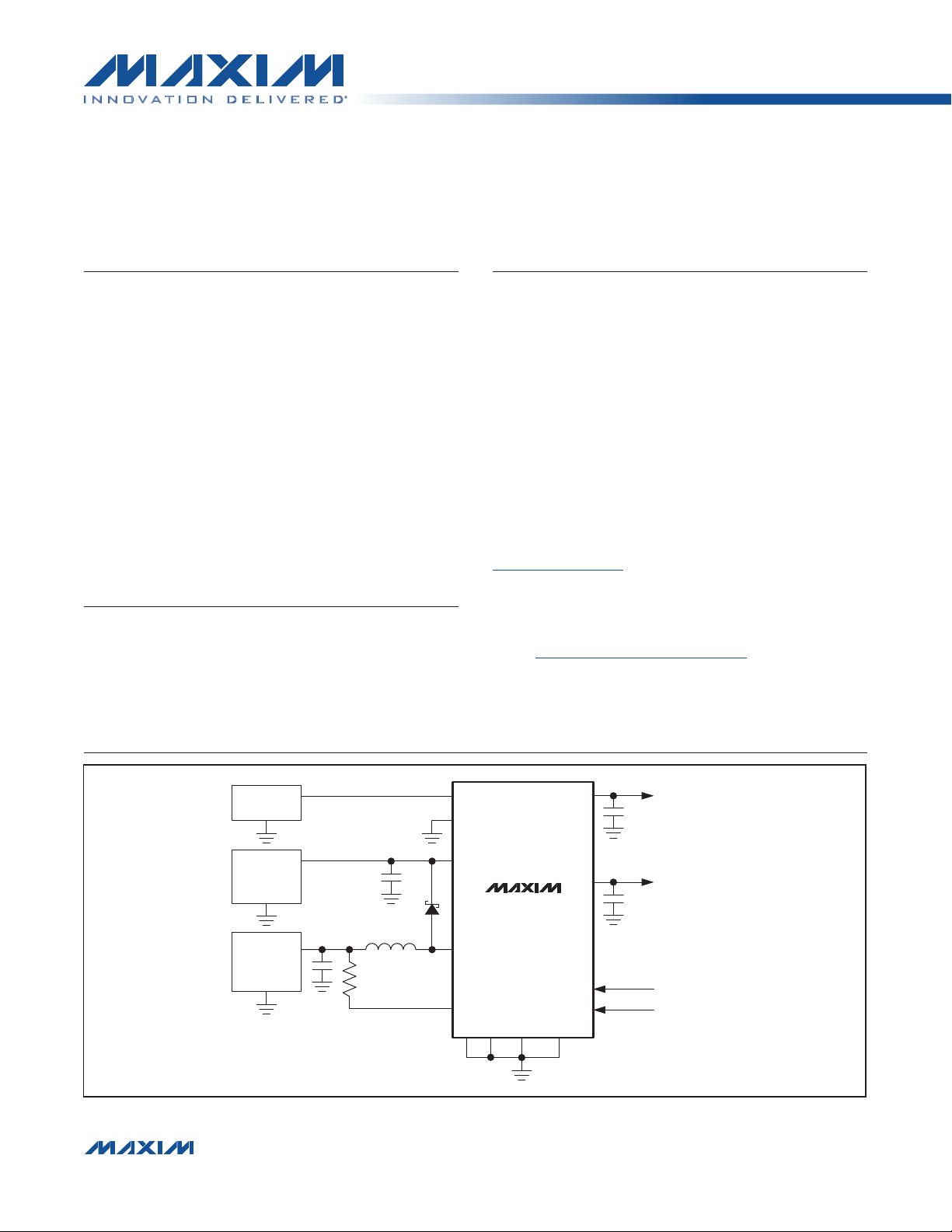
Simplified Operating Circuit
THINERGY
MEC101
RF OR OTHER
HIGH-VOLTAGE
SOURCE
TEG, SOLAR,
OR OTHER
LOW-VOLTAGE
SOURCE
THINERGY is a registered trademark of Infinite Power Solutions, Inc.
����������������������������������������������������������������� Maxim Integrated Products 1
BATT
SEL2
CHG
LX
FB
EP
MAX17710
GND
PCKP
REG
AE
LCE
PGND SEL1
UNREGULATED
OUTPUT
REGULATED
OUTPUT
LDO
CONTROL
SIGNALS
For pricing, delivery, and ordering information, please contact Maxim Direct at 1-888-629-4642,
or visit Maxim’s website at www.maxim-ic.com.
Page 2
MAX17710
Energy-Harvesting Charger and Protector
ABSOLUTE MAXIMUM RATINGS
BATT to GND ........................................................... -0.3V to +6V
CHG to GND ...........................................................-0.3V to +6V
LX to PGND .............................................................-0.3V to +6V
GND to PGND ......................................................-0.3V to +0.3V
FB, AE, LCE, SEL1, SEL2, REG,
PCKP to GND .......................................-0.3V to V
BATT
+ 0.3V
CHG Continuous Current
(limited by power dissipation of package) ...................100mA
Stresses beyond those listed under “Absolute Maximum Ratings” may cause permanent damage to the device. These are stress ratings only, and functional operation of the device at these or any other conditions beyond those indicated in the operational sections of the specifications is not implied. Exposure to absolute
maximum rating conditions for extended periods may affect device reliability.
ELECTRICAL CHARACTERISTICS
(V
= +4.3V, Figure 1, TA = -40NC to +85NC, unless otherwise noted. Typical values are at T
CHG
PARAMETER SYMBOL CONDITIONS MIN TYP MAX UNITS
CHG Input Maximum Voltage Limited by shunt regulator (Note 2) 4.875 5.3 5.7 V
CHG Enable Threshold V
CHG Quiescent Current I
CHG Shunt Delay 25
CHG Input Shunt Limit (Note 2) 50 mA
CHG Maximum Input Current
CHG-to-BATT Dropout Voltage
BATT REG
BATT Regulator Voltage 4.065 4.125 4.160 V
BATT Regulation Delay V
BATT Quiescent Current I
CE
QCHGVCHG
V
CHG
Maximum Ratings
V
CHG
V
CHG
V
CHG
V
CHG
CHG
Regulator in dropout;
V
CHG
Harvest standby (AE pulse low)
V
QBATT
CHG
AE regulator on, boost off;
V
CHG
LCE regulator on, boost off;
V
BATT
= 4.0V rising, V
input current limited by Absolute
= 4.0V, I
= 4.0V, I
= 4.0V, I
= 4.0V, I
= 4.2V, starting at 4V 30
= 4.15V, V
= 0V, V
= 0V, V
= 4.0V, LCE mode (Note 3)
Continuous Power Dissipation (TA = +70NC)
12-Pin UTDFN (derate 15mW/NC above +70NC) .......1200mW
Operating Temperature Range .......................... -40NC to +85NC
Junction Temperature .....................................................+150NC
Storage Temperature Range ............................ -65NC to +150NC
Lead Temperature (soldering, 10s) ................................+300NC
Lead Temperature (reflow) ..............................................+260NC
= +25NC.) (Note 1)
A
4.07 4.15 4.21 V
= 4.0V 625 1300 nA
BATT
50 100 mA
= 1FA
CHG
= -6mA 55
BATT
= -20mA 65
BATT
= -40mA 100
BATT
= 4.12V
BATT
= 2.1V to 4.0V
BATT
= 4.0V, AE high
BATT
45
450 1030
1 165
725 1650
150 550
Fs
mV
Fs
nA
����������������������������������������������������������������� Maxim Integrated Products 2
Page 3
MAX17710
Energy-Harvesting Charger and Protector
ELECTRICAL CHARACTERISTICS (continued)
(V
= +4.3V, Figure 1, TA = -40NC to +85NC, unless otherwise noted. Typical values are at T
CHG
PARAMETER SYMBOL CONDITIONS MIN TYP MAX UNITS
LINEAR LDO REGULATOR
V
REG Voltage
REG Voltage, LCE Mode
(Note 3)
REG Current Limit
PCKP
V
PCKP
V
PCKP
V
PCKP
V
PCKP
V
PCKP
V
REG
V
REG
= 4.0V, I
= 4.0V, I
= 4.0V, I
= 4.0V, I
= 4.0V, I
= 4.0V, I
= 2.15V, V
= 2.15V, V
= 50FA, SEL1 = open
REG
= 50FA, SEL1 = GND
REG
= 50FA, SEL1 = BATT
REG
= 50FA, SEL1 = open
REG
= 50FA, SEL1 = GND
REG
= 50FA, SEL1 = BATT
REG
= 3.8V, AE high 75 mA
PCKP
= 3.8V, LCE mode
PCKP
(Note 3)
REG Startup Time
V
= 4.0V, AE rising, C
PCKP
REG
= 1FF
SEL1 = open 2.175
LCE Threshold High (Note 4) V
IH-LCE
SEL1 = BATT 1.30
SEL1 = open 0.9
LCE Threshold Low (Note 5) V
IL-LCE
SEL1 = BATT 0.5
PCKP REGULATOR
AE Threshold High V
AE Threshold Low V
AE Low Input Current
IH-AE
IL-AE
VAE = 0V, persists < 1Fs
VAE = 0V, persists > 1Fs
AE High Input Current VAE = 3.6V 1 nA
PCKP Enable Threshold REG enabled 3.62 3.7 3.78 V
PCKP Charge Current V
PCKP Impedance Ramp Rate
BATT Undervoltage Lockout
(UVLO) Delay
BATT UVLO Delay t
t
UVLO1
UVLO2
BATT UVLO Threshold
= 0V, V
PCKP
V
= 4.0V, resistance between BATT
BATT
= 2.2V 100 mA
BATT
and PCKP from high impedance to 5I
V
= 2.15V, AE high, first ramp of
BATT
PCKP
V
= 2.15V, AE high, not first PCKP
BATT
ramp
AE regulator active, LCE regulator inactive 1.990 2.15 2.30
LCE regulator active, AE regulator inactive 3
= +25NC.) (Note 1)
A
3.22 3.3 3.37
2.25 2.3 2.375
1.75 1.8 1.9
2.9 3.3 3.7
2.1 2.3 2.5
1.6 1.8 2.05
50
5.3 ms
1.13 V
0.15 V
-4 -2
1 nA
5 ms
5 s
0.5 ms
V
V
FA
VSEL1 = GND 1.575
VSEL1 = GND 0.6
FA
V
����������������������������������������������������������������� Maxim Integrated Products 3
Page 4
MAX17710
Energy-Harvesting Charger and Protector
ELECTRICAL CHARACTERISTICS (continued)
(V
= +4.3V, Figure 1, TA = -40NC to +85NC, unless otherwise noted. Typical values are at T
CHG
PARAMETER SYMBOL CONDITIONS MIN TYP MAX UNITS
BOOST REGULATOR
CHG Regulation Voltage V
Frequency V
Boost Turn-On Time t
FB Threshold
FB Input Current Low VFB = GND, momentary 600 nA
LX nMOS On-Resistance R
Note 1: Specifications are 100% production tested at TA = +25NC. Limits over the operating temperature range are guaranteed by
design and characterization.
Note 2: Since the CHG shunt regulator has a 25Fs delay, the user must limit the voltage to the Absolute Maximum Rating until the
internal CHG shunt provides the voltage limit at the pin in response to 50mA input. Larger currents must be shunted with
an external clamp to protect the CHG pin from damage.
Note 3: LCE mode is entered by pulsing AE high, then pulsing AE low.
Note 4: For logic-high, connect LCE to the REG output. Do not connect to the BATT or PCKP pins.
Note 5: Since LCE is compared to the REG pin voltage for operation, the low-power regulator cannot be switched off under condi-
tions where the REG output is shorted to GND.
BOOST-ON
FB
ON
FB
OFF
DS-ON
= 4.125V 4.3 4.5 4.7 V
BATT
= 3.9V, V
BATT
Design guidance, typical only 850 ns
Rising (enable) 0.485 0.75 1.0
Falling (disable), V
I
= 20mA, V
LX
ILX = 10mA, V
= 3.95V 0.73 1 1.27 MHz
CHG
= 3.8V 0.22 0.25 0.27
CHG
= 3.8V, SEL2 = GND 0.275 0.5 0.7
BATT
= 3.8V, SEL2 = open 4 8 12
BATT
= +25NC.) (Note 1)
A
V
I
����������������������������������������������������������������� Maxim Integrated Products 4
Page 5
MAX17710
Energy-Harvesting Charger and Protector
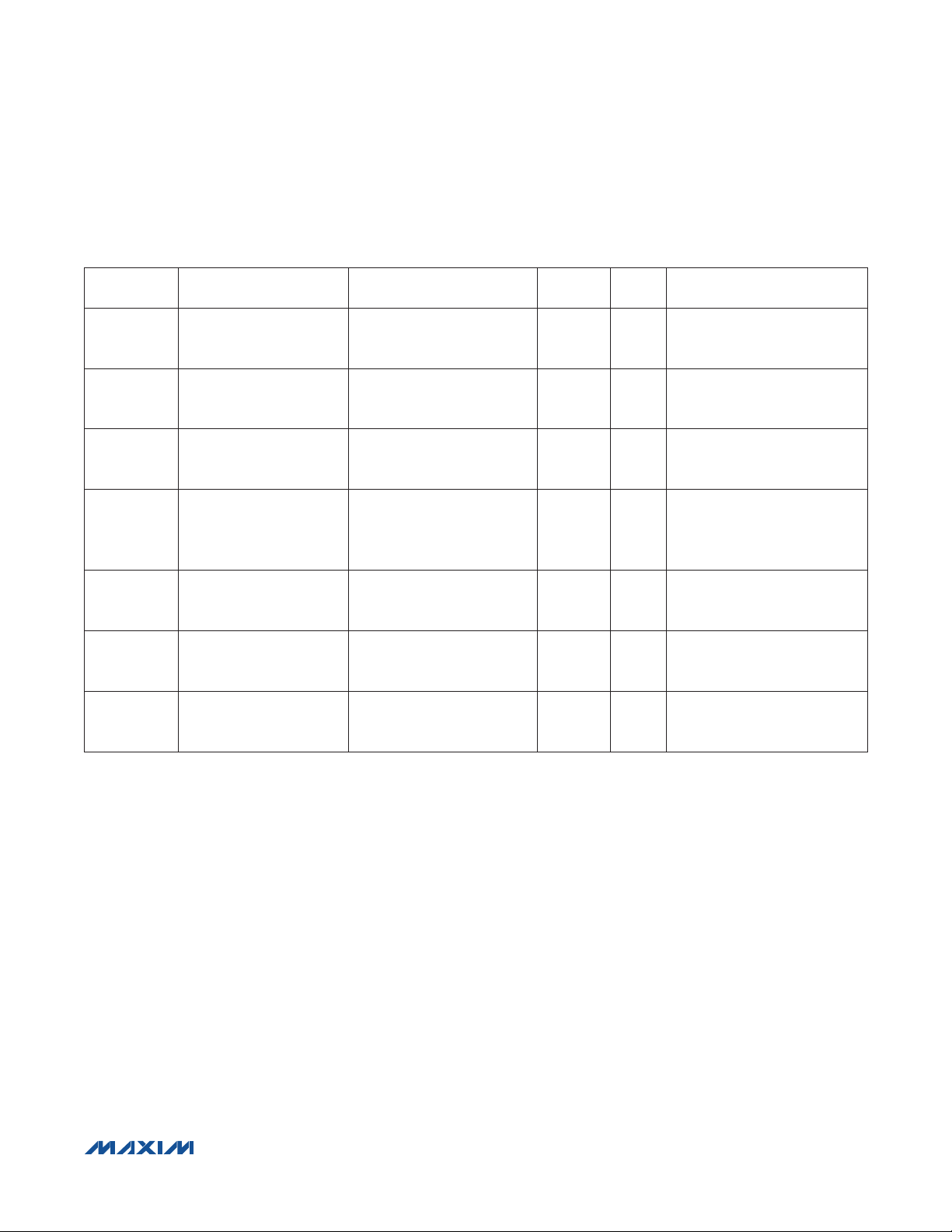
Table 1. Summary of Typical Quiescent Current vs. Operating Conditions
NAME MODE CONDITIONS
Standby
Shutdown
Full Charge
Dropout
Charge
AE Active
AE and LCE
Active
LCE Active
Cell Connection:
Regulator outputs off,
no charger present
UVLO or Shutdown:
Regulator outputs off,
no charger present
Charger Present:
Regulator outputs off,
cell charging
Charger in Dropout:
Regulator outputs off,
charger present, but
below regulation voltage
AE Regulator On:
Boost off, no charge
source present
AE and LCE Regulators
On: Boost off, no charge
source present
LCE Regulator On:
Boost off, no charge
source present
Cell connected to circuit
during assembly
V
falls below 2.15V
BATT
or AE and LCE pulsed low
V
= 4V,
CHG
V
> V
CHG
AE pulsed low
V
CHG
V
BATT
AE pulsed low
AE pulsed high 725 — 725 (from cell)
LCE pulsed high after AE
pulsed high
AE pulsed high, then LCE
pulsed high, then AE pulsed
low
BATT,
= 4.15V,
= 4.12V,
I
QBATT
(nA)
1 — 1 (from cell)
1 — 1 (from cell)
1 625
450 — 450 (from cell)
875 — 875 (from cell)
150 — 150 (from cell)
I
QCHG
(nA)
TOTAL QUIESCENT
CURRENT (nA)
626 (from energy-harvesting
cell); can harvest down to
1µW
����������������������������������������������������������������� Maxim Integrated Products 5
Page 6
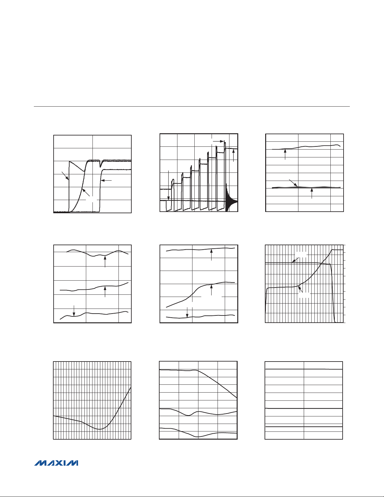
Energy-Harvesting Charger and Protector
(TA = +25°C, unless otherwise noted.)
6
5
4
3
VOLTS (V)
2
1
0
190
170
150
(nA)
DD
I
130
110
90
3.0
1.0
0.9
0.8
0.7
0.6
0.5
0.4
0.3
HARVEST SOURCE POWER (µW)
0.2
0.1
0
3.5 3.7 4.14.03.6
REGULATOR STARTUP
AE
REG
PCKP
0 10
IDD vs. V
5
TIME (ms)
OVERTEMPERATURE
BATT
LCE = VREG, AE, AND SEL1 = GND
T
= +85°C
A
V
BATT
TA = +25°C
4.03.5
(V)
= -40°C
T
A
BOOST CIRCUIT BREAK-EVEN
THRESHOLD vs. CELL VOLTAGE
(STANDARD APPLICATION CIRCUIT)
3.93.8
V
(V)
BATT
6
MAX17710 toc01
MAX17710 toc04
MAX17710 toc07
5
4
3
VOLTS (V)
2
1
0
825
775
725
(nA)
675
DD
I
625
575
525
3.5
3.3
3.1
2.9
2.7
2.5
2.3
2.1
REGULATOR VOLTAGE (V)
1.9
1.7
1.5
Typical Operating Characteristics
BOOST STARTUP
LX
SOLAR
0
IDD vs. V
TIME (µs)
OVERTEMPERATURE
BATT
AE = BATT, LCE, AND SEL1 = GND
TA = +85°C
= -40°C
V
BATT
TA = +25°C
(V)
T
A
AE LOAD REGULATION
0 200
LOAD (mA)
CHG
8642
4.03.53.0
15010050
MAX17710
IDD vs. V
LCE AND AE AND SEL1 = GND
10
(nA)
DD
I
9
8
7
T
6
5
4
3
2
1
0
3.0
MAX17710 toc02
MEC101 CELL CHARGE PROFILE
4.15 0.50
4.10
MAX17710 toc05
4.05
4.00
3.95
3.90
CELL VOLTAGE (V)
3.85
3.80
3.75
0 50 100 150 200 250
3.5
3.3
MAX17710 toc08
3.1
2.9
2.7
2.5
2.3
2.1
REGULATOR VOLTAGE (V)
1.9
1.7
1.5
0
OVERTEMPERATURE
BATT
= +85°C
A
= +25°C
T
A
= -40°C
T
A
V
(V)
BATT
2.5mW CHARGE SOURCE
I
BATT
V
BATT
TIME (Minutes)
LCE LOAD REGULATION
LOAD (µA)
4.03.5
MAX17710 toc06
10050
MAX17710 toc03
0.45
0.40
CHARGE CURRENT (mA)
0.35
0.30
0.25
0.20
0.15
0.10
0.05
0
MAX17710 toc09
����������������������������������������������������������������� Maxim Integrated Products 6
Page 7

MAX17710
Energy-Harvesting Charger and Protector
Pin Configuration
TOP VIEW
+
BATT
1
PCKP
12
CHG
2
FB
3
LCE
11
REG
10
MAX17710
GND
PGND
4
LX
5
6
EP
SEL1
9
SEL2
8
AE
7
UTDFN
Pin Description
PIN NAME FUNCTION
1 BATT Cell Input. Connect to the positive terminal of the cell without a bypass capacitor.
2 CHG
3 FB
4 GND Device Ground. Connect to system ground.
5 LX Boost Input. Controls current drive through inductor of external boost circuit.
6 PGND Power Ground. Connect to system ground.
7 AE
8 SEL2
9 SEL1
10 REG
11 LCE
12 PCKP
— EP Exposed Pad. Connect to GND.
Charge Input. The IC charges the cell from the power source applied to this pin. Connect to the
output of the boost circuit or directly to a 4.21V or higher charge source.
Boost Enable. The boost circuit is enabled by driving this pin above the FBON threshold. Afterwards,
the boost circuit is disabled by driving this pin below FB
OFF
.
Active Enable. Pulse high to enable high-power regulator output. Pulse low to disable regulator
output.
Boost R
Select. Connect to system ground to select a boost R
DS-ON
of 0.5I for typical
DS-ON
applications.
Regulator Voltage Select. Ground this pin to select a regulator output voltage of 2.3V, leave
disconnected for a regulator output voltage of 3.3V, or connect to the BATT pin for a regulator
output voltage 1.8V.
Regulator Output. Connect to load circuit. Bypass to system ground with a 1FF (typ) capacitor.
Low-Current Enable. Pulse high to enable the low-current regulator output after the high-current
regulator output is already active. Pulse low to disable.
Protected Output of Pack. Connect an external capacitor to PCKP to support energy buffering to
the load, especially in low-temperature applications (see Table 4). PCKP is used for pulsed current
storage.
����������������������������������������������������������������� Maxim Integrated Products 7
Page 8

MAX17710
Energy-Harvesting Charger and Protector
Block Diagram
THINERGY
MEC101
RF, SOLAR,
OR OTHER
HIGH-VOLTAGE
SOURCE
47µF
300kI
0.1µF
ZLLS410TA
TEG, SOLAR,
OR OTHER
LOW-VOLTAGE
SOURCE
1.5µH
BATT
CHG
PGND
SEL2
LX
5.3V SHUNT
PROTECTION
TO REJECT
OVERCHARGE
LINEAR CHARGE
AND IDEAL
DIODE CONTROL
BATT
BOOST REG
DISABLE
OVERDISCHARGE
AND UNDERVOLTAGE
PROTECTION
REF
STATE
MACHINE
MAX17710
OUTPUT
LINEAR REG
3.3V/2.3V/1.8V
SELECT
PCKP
REG
SEL 1
AE
UNREGULATED
OUTPUT
10µF
LOAD V
DD
1.0µF
EVENT
DETECTOR
MECHANICAL, RF,
PIEZO, OR OTHER
LOAD V
DD
FB
ON
THRESHOLD
FB
LCE
GND
MICROCONTROLLER
����������������������������������������������������������������� Maxim Integrated Products 8
Page 9

MAX17710
Energy-Harvesting Charger and Protector
Detailed Description
Operation
The MAX177710 controls two main functions related to
management of an energy-harvesting application: charging
a low-capacity cell with overcharge protection and an LDO
regulator output with overdischarge protection. With the
exception of protection features, charging and regulation
functions operate completely independently of one another.
Initial power-up of the device occurs when a cell is connected to the BATT pin. In this state, the device pulls only
1nA (typ) from the cell and LDO functions are disabled. Only
after a charger has been applied and V
4.15V (VCE) does the device initialize to full operation and
allow discharging.
Charge-Regulator Operation
The device charges the cell from an external energy
source connected to the CHG pin. Whenever the voltage on CHG is greater than the voltage on BATT, the
energy-harvesting circuit directly passes current to the
cell without any interaction from the device. When CHG
rises above VCE, the input linear regulator turns on to limit
the charging voltage to 4.125V and protects the cell from
overcharge. Also at this time, any UVLO is reset, allowing the LDO to power the application load. This release
of the lockout is latched by CHG exceeding VCE and
rises above
CHG
remains active after the removal of the charge voltage.
The state of this latch is off when initial power is applied
to the BATT pin.
While charging, the device consumes approximately
625nA from the CHG source until the voltage on CHG
exceeds 4.15V. Above 4.15V, the IC enters dropout and
BATT quiescent current increases from 1nA to 450nA.
CHG Shunt
Whenever a harvest source pulls the CHG pin above
5.3V, an internal shunt regulator enables a path to GND
to limit the voltage at the CHG pin. The internal shunt
path can sustain currents up to 50mA. If it is possible for
the harvest source to exceed this power limit, an external
protection circuit is required to prevent damage to the
device. Figure 1 shows the typical application charge circuit harvesting from high-voltage charge sources. Note
that a 0.22FF on CHG is recommended for shunt stability
when charging from high-voltage sources.
In the application circuit example, the cell is charged by
several high-voltage harvest sources. Whenever either harvest source voltage is higher than the cell voltage, charge
is transferred directly. If either charge source exceeds
4.15V, the device begins to limit current flow to regulate the
cell’s voltage to 4.125V. If either charge source exceeds
5.3V, the internal CHG shunt discharges up to 50mA
through the device to GND to protect the CHG pin.
THINERGY
MEC101
0.22µF
HIGH-VOLTAGE AC
CHARGING SOURCE
(SOLAR, PIEZO)
Figure 1. Typical Application Charge Circuit Harvesting from High-Voltage Charge Sources
����������������������������������������������������������������� Maxim Integrated Products 9
HIGH-VOLTAGE DC
CHARGING SOURCE
(SOLAR, PIEZO)
BATT
SEL2
SEL1
CHG
MAX17710
LX
FB
GND PGND PCKP
EP
REG
AE
LCE
10µF
LOAD V
1µF
DETECTOR
MECHANICAL,
RF, PIEZO,
OR OTHER
LOAD V
MICROCONTROLLER
DD
EVENT
DD
Page 10

MAX17710
Energy-Harvesting Charger and Protector
Boost Regulator Operation
The device includes a simple boost regulator controller to
support energy harvesting from low-voltage solar or thermoelectric generator (TEG) devices. The boost converter
can harvest energy down to approximately 1FW when
operated in pulsed harvest mode and as high as 100mW
in continuous conversion. For a 0.8V harvest source and
a 4.1V cell, the device can deliver over 20mA (80mW), as
long as the harvest source can support it. Figure 2 shows
the typical application boost circuit boost harvesting
from a low-voltage solar-cell array.
In the application circuit example, the solar cell array
charges the 47FF harvest-source capacitor until the voltage on FB exceeds the FBON threshold. At this time, the
LX pin is pulled low to force current through the external
inductor. LX begins to oscillate at a fixed 1.0MHz with
90% duty cycle. Each time LX is released by the device,
the external inductor forces the voltage of LX above CHG
and charges the 0.1FF CHG pin capacitor. When CHG
rises above the voltage of V
, charge is delivered to
BATT
the cell. If the CHG pin exceeds 4.5V during this time,
the boost converter enters a skip-mode operation to
limit voltage on CHG to 4.5V. Operation continues until
the voltage of the harvest-source capacitor collapses,
driving FB below the FB
threshold, which disables
OFF
the boost circuit. The process repeats after the harvest
source capacitor is recharged.
Because the boost converter draws its quiescent current
directly from the cell (for startup reasons), it is important
to only enable the boost converter when it can provide
more power than the boost converter consumes from the
cell. This can be guaranteed as long as the capacitor
across the TEG is large enough to boost CHG above the
BATT pin. Note that it is important to use a high-speed
Schottky diode between LX and CHG to guarantee LX
does not exceed its absolute maximum voltage rating
during boost operation.
Charge Regulator Component Selection
External component selection depends on the charge
sources available to the device. Proper component
selection provides the highest efficiency operation of the
IC during energy harvesting. See Figure 2 as a reference.
This section describes component selection for boost
sources with operational voltages of 1.0V or high-voltage
sources. For boost charge sources with operational voltages between 1.0V and 2.0V, additional components
are required. See the FB Divider section for a detailed
description.
THINERGY
MEC101
0.1µF
ZLLS410TA
HIGH-SPEED
SCHOTTKY
1.5µH
SOLAR CELL 2
SOLAR CELL 1
Figure 2. Typical Application Boost Circuit Boost Harvesting from a Low-Voltage Solar-Cell Array
���������������������������������������������������������������� Maxim Integrated Products 10
47µF
300kI
BATT
SEL2
SEL1
CHG
MAX17710
LX
FB
GND PGNDEP
REG
AE
LCE
PCKP
10µF
LOAD V
DD
1µF
EVENT
DETECTOR
MECHANICAL,
RF, PIEZO,
OR OTHER
LOAD V
MICROCONTROLLER
DD
Page 11

MAX17710
Energy-Harvesting Charger and Protector
CHG Capacitor
The CHG pin capacitor should be minimized to 0.1FF
for highest charge efficiency. However, when charging
from a high-voltage source, at least 0.22FF is required
for shunt stability.
LX Inductor
The LX pin inductor is not required for high-voltage
charge sources. For low-voltage sources, a minimum
inductor value of 0.68FH is required to prevent the maximum current rating of the LX pin from being exceeded.
Minimum inductor value is calculated as follows:
LX inductor = V
FB-ON
x t
BOOST-ON
/LX
IMAX
= 1.0V x
850ns/1A = 0.85FH
Boost Diode
The boost circuit diode must be a high-speed Schottky,
such as the ZLLS410TA from Diodes Incorporated. The
diode must turn on quickly to clamp the LX pin voltage rise at 6.0V or lower when the LX driver turns off.
The LX pin can be damaged if the maximum voltage is
exceeded.
Harvest Source Capacitor
The harvest source capacitor must be a minimum of 70
times larger than the CHG pin capacitor to boost the
charge pin to the maximum charge voltage under worstcase conditions:
Source capacitor = (4.125V)2/(0.485V)2 x
CHG capacitor
This is the minimum size required for operation. Increasing
the size of the harvest source capacitor beyond this
level improves charge circuit efficiency at extremely low
input power (< 10FW), but care should be taken not to
increase the capacitor so large that the harvest source
cannot overcome the capacitor’s leakage. A maximum
value of 47FF is recommended.
Table 2 lists boost converter external component values.
Minimum capacitor and inductor values are required for
proper operation of the charge circuit. Recommended
capacitor and inductor values provide optimum charge
efficiency. Components should be sized as close to
the recommended values that the application allows.
Component values below the minimum values, or above
the optimum values, are not recommended.
FB Divider
Charge sources with operational voltages between 1.0V
and 2.0V require boosting, but are too high a voltage to
control the boost circuit efficiently. Under these conditions, a voltage-divider is required to lower the voltage
seen by the FB pin (see Figure 3). The divider formed by
R1 and R2 allows the voltage on the FB pin to transition
properly between the FBON and FB
thresholds during
OFF
boosting. The value for R2 is calculated as follows:
where V
V
HARVEST-ON
R2 = (V
HARVEST-ON
= F
HARVEST-ON
x (R1 + R2)/R1
BON
- 1.0V) x 500kI
is the operational voltage of the
harvest source.
Table 2. Boost Converter External Component Values
APPLICATION
CHARGE SOURCE
High voltage 0.22 N/A N/A N/A N/A
Low voltage < 10FW
Low voltage > 10FW
High voltage and low
voltage < 10FW
High voltage and low
voltage > 10FW
���������������������������������������������������������������� Maxim Integrated Products 11
CHG
CAPACITOR
(µF)
0.1 0.85 1.5 7.0 47
0.1 0.85 1.5 7.0 7.0
0.22 0.85 1.5 15.4 47
0.22 0.85 1.5 15.4 15.4
MINIMUM LX
INDUCTOR
(µH)
RECOMMENDED
LX INDUCTOR
(µH)
MINIMUM
HARVEST SOURCE
CAPACITOR (µF)
RECOMMENDED
HARVEST SOURCE
CAPACITOR (µF)
Page 12

Energy-Harvesting Charger and Protector
The C1 1nF capacitor acts as a voltage-level feed forward to increase the responsiveness of the divider circuit
as the harvest source capacitor is discharged. The minimum voltage is defined as:
V
HARVEST-OFF
V
HARVEST-OFF
where V
HARVEST-OFF
source capacitor during boost.
Because of the divider on the FB pin, the voltage seen by
the LX pin inductor is higher than the typical circuit. The
inductor must be resized so that the LX pin current limits
are not exceeded:
LX Inductor = V
All other components are selected as normal.
Energy-Harvesting Design Approaches
When designing an optimal energy harvest system,
there are three types of design approaches: linear harvest, boost harvest, and maximum-power-point tracking
(MPPT). In harvesting applications, it is very critical to
not discharge the cell when charging is failing. When
the harvesting power is low enough, eventually the system discharges the cell rather than charges. This is the
break-even point of the harvester. For linear harvesting,
this break-even point is lower because the required
quiescent current is less. However, for boost harvesting,
the breakeven threshold is 1FA. While an MPPT system
can utilize the harvesting source more intelligently in
high-power situations, it inevitably results in higher quiescent current and a poorer break-even threshold. MPPT
systems must measure the current and voltage, multiply
to determine power, and make decisions to improve the
power. These required measurements automatically
significantly increase the quiescent current budget
by tens of µA. Figure 4 shows energy-harvesting modes
of operation vs. charge efficiency.
~= V
~= V
HARVEST-ON
HARVEST-ON
- (FBON - FB
- 0.5V (typ)
is the lowest voltage of the harvest
HARVEST-ON
V
HARVEST-ON
x t
BOOST-ON
x (8.5 x 10⁻⁷)
/LX
OFF
IMAX
)
=
MAX17710
CHG
0.1µF
ZLLS410TA
1.0V TO 2.0V
CHARGE
SOURCE
47µF
Figure 3. FB Divider Circuit to Improve Boost Efficiency for
Charge Sources Between 1.0V and 2.0V
BREAK-EVEN
CHARGE EFFICIENCY
THRESHOLDS
C1
1nF
500kI
LINEAR
HARVEST
R1
L1
R2
MAX17710
LX
FB
MPPT
(MAX POWER
TRACKING)
BOOST HARVEST
LDO Output Operation
The device regulates voltage from the cell to a load
circuit on the REG pin through an LDO regulator. The
regulator can be configured for 3.3V, 2.3V, or 1.8V operation. The LDO supports loads up to 75mA (high-current
mode). For lighter load applications, a low-power mode
of operation reduces the quiescent current drain on the
cell. A UVLO circuit prevents the regulator from starting up or disabling the regulator when active if the cell
becomes overdischarged.
���������������������������������������������������������������� Maxim Integrated Products 12
POWER FROM HARVEST SOURCE
Figure 4. Energy-Harvesting Modes of Operation vs. Charge
Efficiency
Page 13

MAX17710
Energy-Harvesting Charger and Protector
The LDO becomes active when the AE pin is pulsed
above or held above its logic-high threshold, but the
regulator output is not immediately enabled. The device
first charges the external capacitor on PCKP. When the
voltage level on PCKP reaches 3.7V, the regulator output
is enabled in high-current mode. Powering the LDO from
PCKP instead of directly from the cell allows the device
to support large surge or startup inrush currents from the
load that the cell would be unable to handle directly.
Once in high-current mode, the AE pin can remain logichigh or transition to an open state, and the ouput remains
active. The LDO returns to shutdown only when the AE
pin is driven below its logic-low threshold. Alternatively,
the LDO is transitioned to low-current mode by pulsing
or holding the LCE to the REG pin voltage, followed by
pulsing or holding the AE pin logic-low. Note that the regulator transitions through a state where both high-current
and low-current modes are active at the same time. While
in low-current mode, the quiescent current drain of the
cell is reduced to 150nA, while the maximum load current
able to be supplied becomes 50FA. Similar to the AE pin
operation, the regulator remains active if the LCE pin is
SHUTDOWN
PCKP OFF
I
QBATT
REG OFF
= 1nA (typ)
AE PULSED LOW
open or pulled to REG, and returns to shutdown mode
when LCE is driven below its logic-low threshold. Figure
5 is the regulator output state diagram.
Cell Undervoltage Lockout (UVLO)
If the cell and PCKP capacitance cannot provide sustained support for the load, then the voltage at PCKP collapses. When PCKP collapses, the system load typically
stops and allows the PCKP voltage to recover, resulting
in a perpetual retry in a futile attempt to support a load
that cannot be supported. When PCKP fails in this way,
the device shuts off the REG output to prevent futile load
retries and protect the cell from overdischarge. When the
REG output is latched off, the BATT quiescent current
reduces to 1nA (typ). Once UVLO occurs, the regulator
output remains disabled until the device detects that a
charge source has been connected to the system (V
CHG
> 4.15V). Figure 6 shows the UVLO protection modes.
Connecting any load to REG or PCKP instead of connecting directly to the cell is highly recommended. This controls the quiescent current during shutdown, enables the
device to support startup during cold, and also protects
the cell from overdischarge.
LCE PULSED LOW
AE PULSED HIGH
< 2.15V
STARTUP
SUCCESS
V
PCKP
> 3.7V
CHARGE
DETECTED
VCHG > VCE
STARTUP
PCKP ON
REG OFF
= PCKP CAPACITOR
I
QBATT
CHARGE CURRENT
+ 725nA (typ)
STARTUP FAIL
V
PCKP
AFTER 5s
UNDERVOLTAGE
LOCKOUT
PCKP OFF
REG OFF
= 1nA (typ)
I
QBATT
POWER-ON RESET (POR)
Figure 5. Regulator Output State Diagram
���������������������������������������������������������������� Maxim Integrated Products 13
AE REGULATOR
ACTIVE
PCKP ON
REG ON
I
= 725nA (typ)
QBATT
LCE PULSED
HIGH
LCE PULSED
LOW
AE AND LCE
REGULATORS ACTIVE
PCKP ON
REG ON
I
= 875nA (typ)
QBATT
CELL UNDERVOLTAGE
< 2.15V (HIGH-CURRENT MODE)
V
PCKP
V
< 3.0V (LOW-CURRENT MODE)
PCKP
AFTER 500µs
AE PULSED
LOW
AE PULSED
HIGH
LCE REGULATOR
ACTIVE
PCKP ON
REG ON
I
= 150nA (typ)
QBATT
Page 14

BATT
PCKP
REG
MAX17710
Energy-Harvesting Charger and Protector
4.1V
2.15V
4.1V
2.15V
0V
4.1V
3.7V
0V
V
OH-AE
AE
V
OL-AE
3.3V
0V
BATT
PCKP
UVLO
0V
4.1V
0V
V
OH-AE
AE
V
OL-AE
0V
> t
UVLO1
(5s typ)
a. NORMAL REGULATOR OUTPUT ENABLE SEQUENCE
4.1V
BATT
2.15V
0V
4.1V
PCKP
2.15V
0V
3.3V
REG
0V
4.1V
UVLO
0V
c. HIGH-CURRENT MODE REGULATOR OUTPUT DISABLED DUE TO UVLO TIMEOUT
> t
UVLO2
(500µs typ)
Figure 6. ULVO Protection Modes
b. REGULATOR OUTPUT ENABLE FAIL DUE TO UVLO TIMEOUT
4.1V
BATT
3.0V
PCKP
UVLO
d. LOW-CURRENT MODE REGULATOR OUTPUT DISABLED DUE TO UVLO DETECTION
REG
0V
3.3V
0V
0V
���������������������������������������������������������������� Maxim Integrated Products 14
Page 15

MAX17710
Energy-Harvesting Charger and Protector
Regulator Voltage Selection
The SEL1 pin selects at which voltage REG operates.
Connect SEL1 to BATT for 1.8V operation, three-state for
3.3V operation, or connect to GND for 2.3V operation.
Note that the voltage regulation value is latched when
enabled. To change the regulation voltage point, the regulator must be disabled and then reenabled. See Table 3.
PCKP Pin Capacitor Selection
There are several cases when the system might overload
the cell, potentially causing damage. They are prevented
with the PCKP load switch block and external capacitor:
U During startup, when there is an inrush current due to
the application’s load and capacitance.
U When the cell is cold (such as -40NC), and due to
increased cell resistance, it is unable to support highload currents.
U If the system requires a load current higher than can be
supported by the cell alone.
The device provides cell undervoltage protection by
limiting the current from BATT to PCKP and guaranteeing that the cell voltage does not fall below 2.15V. In
addition to voltage protection, the ramp of the PCKP
switch impedance is changed slowly (5ms to full on) to
gradually load the cell and not collapse the voltage on a
room-temperature cell. Because of these protection features, an application can now support brief high-current
pulses by including a large capacitance at PCKP. This
allows support for pulse loads many times higher than
that naturally supported by the cell alone.
A large PCKP capacitance can be selected to support
a pulse load even while the cell is very cold, and would
normally be incapable of supporting a significant load.
Choose this capacitor according to Table 4 or the following equation:
C
PCKP
= I
TASK
x t
TASK
/(3.7 - V
MIN
)
where:
I
is the current required to sustain a required task,
TASK
t
is the time duration of the task, and V
TASK
MIN
is the
minimum voltage of the load doing the task.
This equation assumes that the BATT impedance is high
and cannot support the load.
Table 3. Regulator Output Voltage Selection
SEL1 PIN CONNECTION REG PIN OUTPUT VOLTAGE (V)
Connect to BATT 1.8
Open circuit 3.3
Connect to GND 2.3
Table 4. PCKP Pin Capacitor Values by Application
V
MIN
3.0 5 8 100
3.0 5 4 50
2.8 5 5 28
2.8 5 2.5 14
2.3 5 5 18
2.3 5 10 36
*Capacitance value tolerances need to be considered.
���������������������������������������������������������������� Maxim Integrated Products 15
t
(ms) I
TASK
(mA) C
TASK
PCKP
(µF)*
Page 16

MAX17710
Energy-Harvesting Charger and Protector
Package Information
For the latest package outline information and land patterns
(footprints), go to www.maxim-ic.com/packages. Note that a
“+”, “#”, or “-” in the package code indicates RoHS status only.
Package drawings may show a different suffix character, but
the drawing pertains to the package regardless of RoHS status.
PACKAGE
TYPE
12 UTDFN-EP V1233N+1
PACKAGE
CODE
OUTLINE
NO.
21-0451 90-0339
LAND
PATTERN NO.
Ordering Information
PART TEMP RANGE PIN-PACKAGE
MAX17710G+U
MAX17710G+T
+Denotes a lead(Pb)-free/RoHS-compliant package.
U = Signifies tape cut.
T = Tape and reel.
*EP = Exposed pad.
-40NC to +85NC
-40NC to +85NC
12 UTDFN-EP*
12 UTDFN-EP*
���������������������������������������������������������������� Maxim Integrated Products 16
Page 17

MAX17710
Energy-Harvesting Charger and Protector
Revision History
REVISION
NUMBER
0 6/11 Initial release —
1 7/11
REVISION
DATE
DESCRIPTION
Corrections and clarifications made based on customer feedback; added
new TOC #9 and updated two EC table limits
PAGES
CHANGED
3–7, 9, 10, 12–15
Maxim cannot assume responsibility for use of any circuitry other than circuitry entirely embodied in a Maxim product. No circuit patent licenses are implied.
Maxim reserves the right to change the circuitry and specifications without notice at any time. The parametric values (min and max limits) shown in the Electrical
Characteristics table are guaranteed. Other parametric values quoted in this data sheet are provided for guidance.
Maxim Integrated Products, 120 San Gabriel Drive, Sunnyvale, CA 94086 408-737-7600 17
©
2011 Maxim Integrated Products Maxim is a registered trademark of Maxim Integrated Products, Inc.
 Loading...