

Page 1
General Description
The MAX1758 is a switch-mode lithium-ion (Li+) battery
charger that charges one-to-four cells. It provides a regulated charging current accurate to ±10% and a regulated voltage with only a ±0.8% total voltage error at the
battery terminals. The internal high-side switch delivers
a programmable current of up to 1.5A to charge the battery. The built-in safety timer automatically terminates
charging once the adjustable time limit has been
reached.
The MAX1758 regulates the voltage set point and
charging current using two loops that work together to
transition smoothly between voltage and current regulation. An additional control loop monitors the total current drawn from the input source (charging + system),
and automatically reduces battery-charging current,
preventing overload of the input supply and allowing
the use of a low-cost wall adapter.
The per-cell battery regulation voltage is set between
4.0V and 4.4V using standard 1% resistors. The number of cells is set from 1-to-4 by pin strapping. Battery
temperature is monitored by an external thermistor to
prevent charging outside the acceptable temperature
range.
The MAX1758 is available in a space-saving 28-pin
SSOP package. Use the MAX1758EVKIT to help reduce
design time. For a stand-alone charger with a 14V
switch, refer to the MAX1757 data sheet. For a charger
controller capable of up to 4A charging current, refer to
the MAX1737 data sheet.
________________________Applications
Features
♦ Stand-Alone Charger for Up to 4 Li+ Batteries
♦ ±0.8% Battery Regulation Voltage Accuracy
♦ Low-Dropout 98% Duty Cycle
♦ Safely Precharges Near-Dead Cells
♦ Continuous Voltage and Temperature Monitoring
♦ 0.1µA Shutdown Battery Current
♦ Input Voltage Up to 28V
♦ Up to 1.5A Programmable Charge Current
♦ Safety Timer Prevents Overcharging
♦ Input Current Limiting
♦ Space-Saving 28-Pin SSOP
♦ 300kHz PWM Oscillator Reduces Noise
MAX1758
Stand-Alone, Switch-Mode
Li+ Battery Charger with Internal 28V Switch
________________________________________________________________ Maxim Integrated Products 1
19-1752; Rev 1; 1/01
EVALUATION KIT
AVAILABLE
Ordering Information
28 SSOP
PIN-PACKAGETEMP. RANGE
-40°C to +85°CMAX1758EAI
PART
Li+ Battery Packs
Notebook Computers
Hand-Held Instruments
Desktop Cradle Chargers
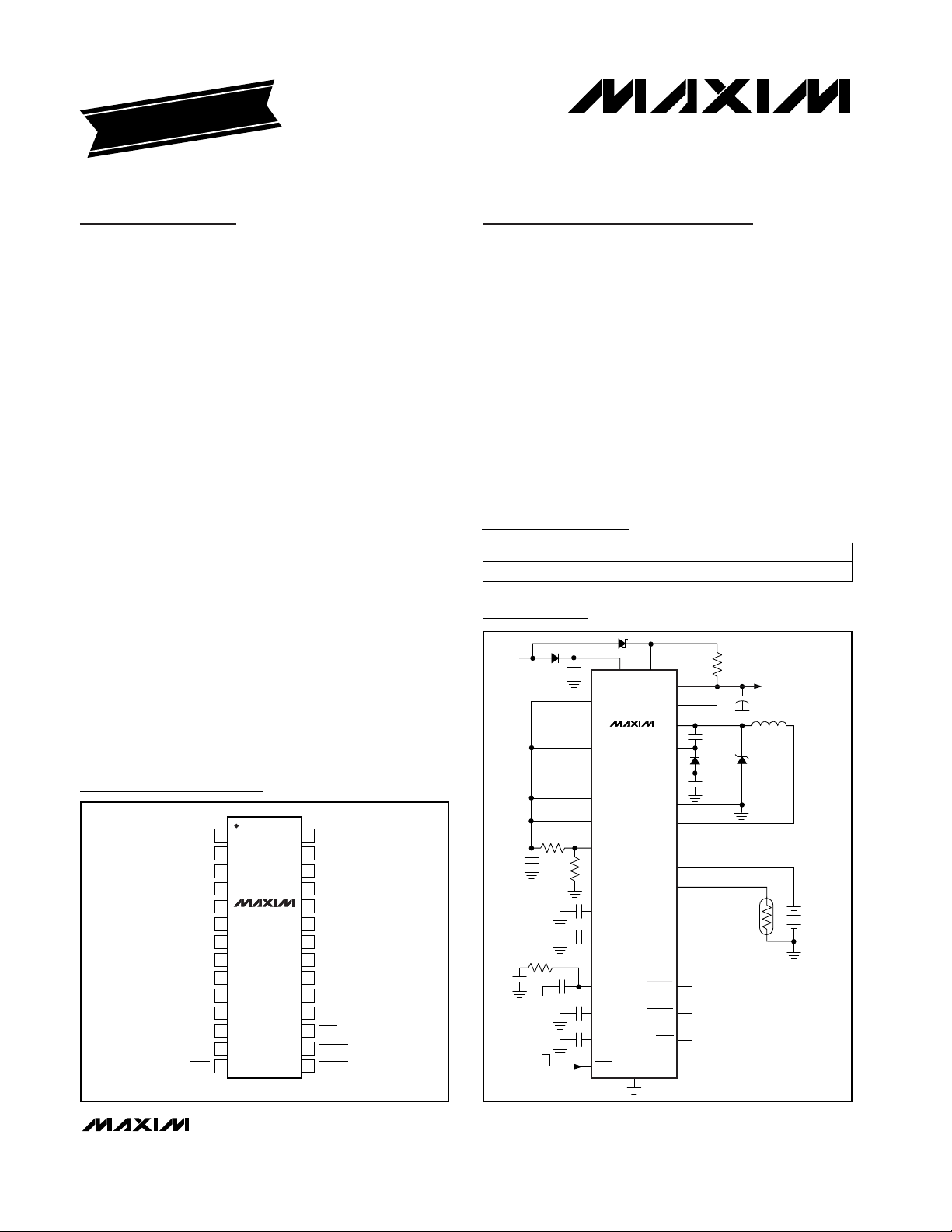
Pin Configuration
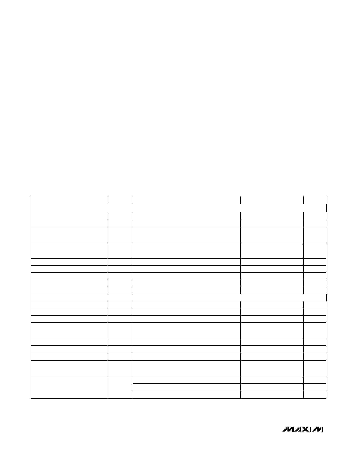
Typical Operating Circuit
For price, delivery, and to place orders, please contact Maxim Distribution at 1-888-629-4642,
or visit Maxim’s website at www.maxim-ic.com.
TOP VIEW
1
VL
2
ISETIN
3
ISETOUT
4
THM
5
REF
6
GND
7
VADJ
8
BATT
9
HSD
10
HSD
11
CELL
12
TIMER1
13
TIMER2
14
FAULT
28
DCIN
27
CSSP
26
CSSN
25
CCV
24
MAX1758
SSOP
23
22
21
20
19
18
17
16
15
CCI
CCS
BST
CS
LX
LX
PGND
SHDN
FULLCHG
FASTCHG
V
IN
6V TO 28V
ON
OFF
REF
ISETOUT
ISETIN
CELL
VADJ
CCS
CCI
CCV
TIMER1
TIMER2
SHDN
DCIN
MAX1758
GND
CSSP
FASTCHG
FULLCHG
FAULT
CSSN
HSD
PGND
BATT
THM
SYSTEM
LOAD
LX
BST
VL
CS
THERM
Li+ BATTERY
1 TO 4 CELLS
Page 2
MAX1758
Stand-Alone, Switch-Mode
Li+ Battery Charger with Internal 28V Switch
2 _______________________________________________________________________________________
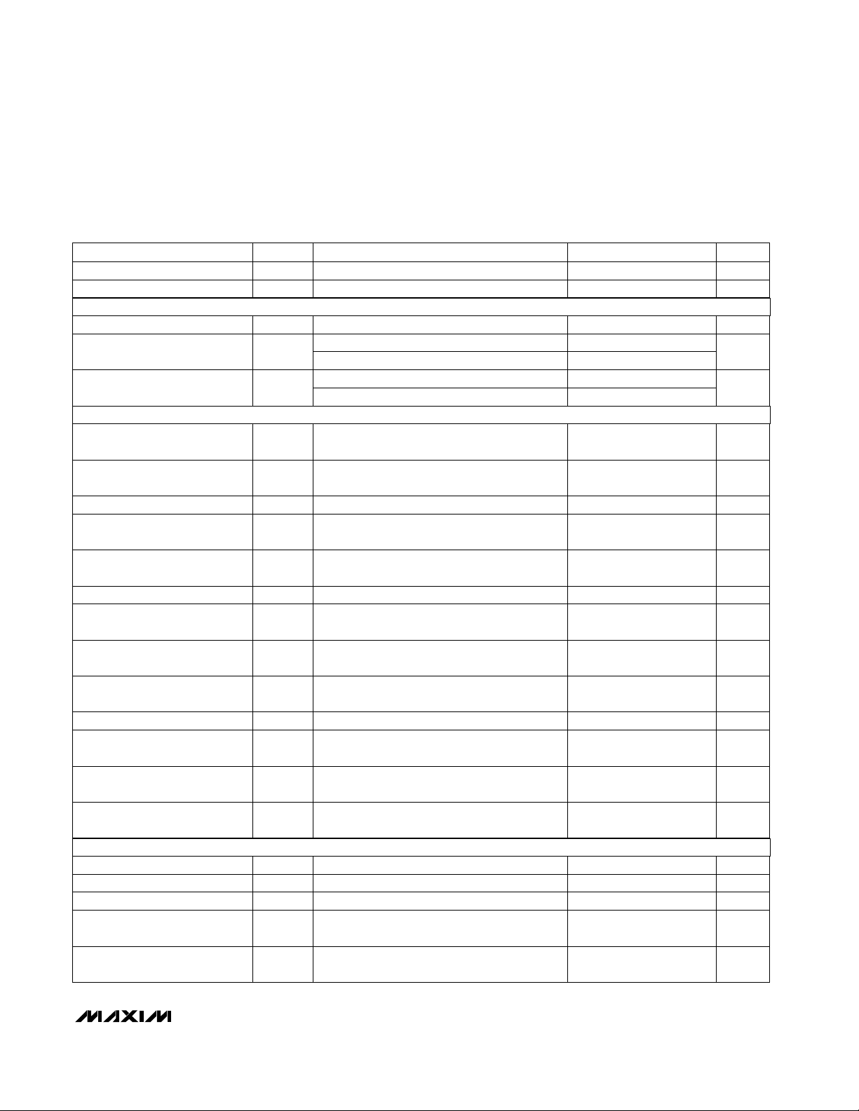
ABSOLUTE MAXIMUM RATINGS
ELECTRICAL CHARACTERISTICS
(Circuit of Figure 1, V
DCIN
= V
HSD
= V
CSSP
= V
CSSN
= 18V, V
SHDN
= VVL, V
CELL
= GND, V
BATT
= VCS= 4.2V, V
VADJ
= V
REF
/ 2,
V
ISETIN
= V
ISETOUT
= V
REF
, R
THM
= 10kΩ, TA= 0°C to +85°C, unless otherwise noted. Typical values are at TA= +25°C.)
Stresses beyond those listed under “Absolute Maximum Ratings” may cause permanent damage to the device. These are stress ratings only, and functional
operation of the device at these or any other conditions beyond those indicated in the operational sections of the specifications is not implied. Exposure to
absolute maximum rating conditions for extended periods may affect device reliability.
DCIN, CSSP, CSSN, HSD to GND..........................-0.3V to +30V
CSSP to CSSN.......................................................-0.6V to +0.6V
BST to GND ............................................................-0.3V to +36V
BST to LX..................................................................-0.3V to +6V
LX to PGND ..............................................-0.6V to (V
HSD
+ 0.3V)
VL, SHDN, ISETIN, ISETOUT, REF, VADJ, CELL, TIMER1,
TIMER2, CCI, CCS, CCV, THM to GND ................-0.3V to +6V
FASTCHG, FULLCHG, FAULT to GND ..................-0.3V to +30V
BATT, CS to GND ...................................................-0.3V to +20V
CS to BATT Current ............................................................±3.5A
PGND to GND .......................................................-0.3V to +0.3V
VL Source Current...............................................................50mA
Continuous Power Dissipation (T
A
= +70°C)
28-Pin SSOP (derate 9.5mW/°C above +70°C) ...........762mW
Operating Temperature Range ...........................-40°C to +85°C
Junction Temperature......................................................+150°C
Storage Temperature.........................................-65°C to +150°C
Lead Temperature (soldering, 10s) .................................+300°C
V
BATT
= 18V, done state
Falling edge
CELL = REF, V
BATT
= 15V, any charging state
V
SHDN
= GND, V
BATT
= 19V
6V < V
DCIN
< 28V
Internal resistor between CS and BATT,
1.5A RMS operating
See PWM Controller section
V
BST
= VLX+ 4.5V
VLX= V
HSD
= V
DCIN
=28V, V
SHDN
= GND
I
REF
= 0 to 1mA
VLX= PGND, V
HSD
= V
DCIN
= 28V,
V
SHDN
= GND
V
CSSN
= V
CSSP
= V
DCIN
= 28V, V
SHDN
= GND
6V < V
DCIN
< 28V
Rising edge
6V < V
DCIN
< 28V
IVL= 0 to 15mA
In-dropout, f
OSC
/ 4
6V < V
DCIN
< 28V
Nondropout f
OSC
CONDITIONS
µA150 270
BATT, CS Input Current
µA280 540
µA0.1 5
mΩ110 170R
CS
CS to BATT Current-Sensing
Resistance
Ω12LX to PGND On-Resistance
mΩ260 450HSD to LX On-Resistance
µA0.1 10LX Off-State Leakage
µA0.1 10HSD Off-State Leakage
µA210CSSN/CSSP Off-State Leakage
%97 98LX Maximum Duty Cycle
kHz270 300 330f
OSC
PWM Oscillator Frequency
V0.075 0.125 0.175
DCIN to BATT Dropout
Threshold, DCIN Falling
mA57DCIN Quiescent Supply Current
mV614REF Load Regulation
mV26REF Line Regulation
V4.179 4.20 4.221
V0.20 0.30 0.40
DCIN to BATT Dropout
Threshold, DCIN Rising
V5.10 5.40 5.70VL Output Voltage
mV44 65
V
REF
REF Output Voltage
UNITSMIN TYP MAXSYMBOLPARAMETER
V628DCIN Input Voltage Range
SUPPLY AND REFERENCE
SWITCHING REGULATOR
VL Output Load Regulation
Page 3
MAX1758
Stand-Alone, Switch-Mode
Li+ Battery Charger with Internal 28V Switch
_______________________________________________________________________________________ 3
ELECTRICAL CHARACTERISTICS (continued)
(Circuit of Figure 1, V
DCIN
= V
HSD
= V
CSSP
= V
CSSN
= 18V, V
SHDN
= VVL, V
CELL
= GND, V
BATT
= VCS= 4.2V, V
VADJ
= V
REF
/ 2,
V
ISETIN
= V
ISETOUT
= V
REF
, R
THM
= 10kΩ, TA= 0°C to +85°C, unless otherwise noted. Typical values are at TA= +25°C.)
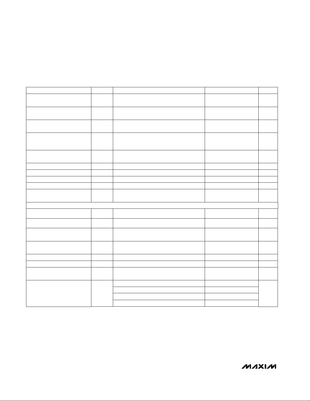
V
ADJ
= GND
Instantaneous peak current limit
With 1% VADJ resistors
Not including VADJ resistor tolerances
CELL = float, GND, VL, or REF
CONDITIONS
3.948 3.979 4.010
BATT Regulation Voltage
Adjustment Range
-1 1
Absolute Voltage Accuracy %
-0.8 0.8
V/cell4.167 4.2 4.233V
BATTR
Battery Regulation Voltage
V019BATT, CS Input Voltage Range
A2.4 2.7 3.0CS to BATT Hard Current Limit
UNITSMIN TYP MAXSYMBOLPARAMETER
V
ADJ
= REF
V/cell
4.386 4.421 4.453
V
CCV
= 2V
mS ×
cells
0.4 0.7 1.0
CCV Amplifier
Transconductance
V
CCV
= 2V µA±50
CCV Amplifier Maximum Output
Current
A1.35 1.5 1.65BATT Full-Scale Charge Current
V
ISETOUT
= V
REF
/ 10 mA100 150 200
BATT 1/10-Scale Charge
Current (Note 1)
V
BATT
< 2.4V per cell mA100 150 200
BATT Charge Current in
Prequalification State
V
CCI
= 2V µA/A60 130 240CCI Battery Current Sense Gain
V
CCI
= 2V µA±100
CCI Amplifier Maximum Output
Current
mV90 100 115
CSSP to CSSN Full-Scale
Current-Sense Voltage
V
ISETIN
= V
REF
/ 10 mV51015
CSSP to CSSN 1/10-Scale
Current-Sense Voltage
V
CCS
= 2V mS1.0 2.0 3.0CCS Amplifier Transconductance
mV25 200
CCV Clamp Voltage with
Respect to CCI, CCS
THM low-temp or high-temp current V1.386 1.40 1.414V
TRT
THM Trip Threshold Voltage
V
THM
= 1.4V µA46.2 49 51.5I
TLTC
THM Low-Temp Current
V
THM
= 1.4V µA344 353 362I
THTC
THM High-Temp Current
Combines THM low-temp current and THM
threshold, V
TRT
/ I
TLTC
kΩ26.92 28.70 30.59
THM COLD Threshold
Resistance (Note 2)
Combines THM high-temp current and THM
threshold, V
TRT
/ I
THTC
kΩ3.819 3.964 4.115
THM HOT Threshold Resistance
(Note 2)
VOLTAGE LIMIT ACCURACY
ERROR AMPLIFIERS
STATE MACHINE
V
CCS
= 2V µA±100
CCS Amplifier Maximum Output
Current
mV25 200
CCI, CCS Clamp Voltage with
Respect to CCV
Page 4
MAX1758
Stand-Alone, Switch-Mode
Li+ Battery Charger with Internal 28V Switch
4 _______________________________________________________________________________________
ELECTRICAL CHARACTERISTICS (continued)
(Circuit of Figure 1, V
DCIN
= V
HSD
= V
CSSP
= V
CSSN
= 18V, V
SHDN
= VVL, V
CELL
= GND, V
BATT
= VCS= 4.2V, V
VADJ
= V
REF
/ 2,
V
ISETIN
= V
ISETOUT
= V
REF
, R
THM
= 10kΩ, TA= 0°C to +85°C, unless otherwise noted. Typical values are at TA= +25°C.)
CONDITIONS
% of
V
BATTR
x cell
94 95 96
BATT Recharge Voltage
Threshold (Note 6)
mA250 330 400
FULLCHG BATT Current
Termination Threshold (Note 5)
V/cell4.55 4.67 4.8
BATT Overvoltage Threshold
(Note 4)
V/cell2.4 2.5 2.6
BATT Undervoltage Threshold
(Note 3)
UNITSMIN TYP MAXSYMBOLPARAMETER
TIMER1 and TIMER2
Oscillation Frequency
2.1 2.33 2.6 kHz
Prequalification Timer 6.25 7.5 8.75
Fast-Charge Timer 81 90 100
Full-Charge Timer 81 90 100
Top-Off Timer 40.5 45 49.8
Temperature Measurement
Frequency
0.98 1.12 1.32 Hz
SHDN Input Voltage High
V
IH
1.4 V
SHDN Input Voltage Low
V
IL
0.6 V
VADJ, ISETIN, ISETOUT Input
Voltage Range
0V
REF
V
V
VADJ
, V
ISETIN
, V
ISETOUT
= 0 or 4.2V nA
SHDN Input Bias Current
V
SHDN
= 0 or V
VL
-1 1 µA
ISETOUT Shutdown Threshold
Voltage (Note 3)
150 220 300 mV
CELL Input Bias Current V
CELL
= 0 or V
VL
-5 5 µA
VADJ, ISETIN, ISETOUT Input
Bias Current
CELL Input Voltage
For 1 cell 0 0.5
For 3 cells V
REF
- 0.3 V
REF
+ 0.3
For 2 cells (floating) 1.5 2.5
-50 50
CONTROL INPUTS/OUTPUTS
min
min
min
min
V
VVL- 0.4 V
VL
For 4 cells
Page 5
MAX1758
Stand-Alone, Switch-Mode
Li+ Battery Charger with Internal 28V Switch
_______________________________________________________________________________________ 5
ELECTRICAL CHARACTERISTICS (continued)
(Circuit of Figure 1, V
DCIN
= V
HSD
= V
CSSP
= V
CSSN
= 18V, V
SHDN
= VVL, V
CELL
= GND, V
BATT
= VCS= 4.2V, V
VADJ
= V
REF
/ 2,
V
ISETIN
= V
ISETOUT
= V
REF
, R
THM
= 10kΩ, TA= 0°C to +85°C, unless otherwise noted. Typical values are at TA= +25°C.)
ELECTRICAL CHARACTERISTICS
(Circuit of Figure 1, V
DCIN
= V
HSD
= V
CSSP
= V
CSSN
= 18V, V
SHDN
= VVL, V
CELL
= GND, V
BATT
= VCS= 4.2V, V
VADJ
= V
REF
/ 2,
V
ISETIN
= V
ISETOUT
= V
REF
, R
THM
= 10kΩ, TA= -40°C to +85°C, unless otherwise noted.) (Note 7)
CONDITIONS
DCIN Input Voltage Range 628V
UNITSMIN TYP MAXSYMBOLPARAMETER
VL Output Voltage 5.1 5.7 V
REF Output Voltage 6V < V
DCIN
< 28V 4.166 4.242 V
REF Line Regulation 6V < V
DCIN
< 28V 6 mV
PWM Oscillator Frequency f
OSC
Nondropout f
OSC
260 340 kHz
HSD to LX On-Resistance V
BST
= VLX+ 4.5V 450 mΩ
LX to PGND On-Resistance 2 Ω
CS to BATT Hard Current Limit Instantaneous peak current limit 2.2 3.2 A
BATT, CS Input Voltage Range 019V
Absolute Voltage Accuracy
Not including VADJ resistor tolerances -0.8 0.8
%
With 1% VADJ resistors -1 1
CSSP to CSSN 1/10-Scale
Current-Sense Voltage
V
SETIN
= V
REF
/ 10 515mV
THM Trip Threshold Voltage V
TRT
THM low- temp or high-temp current 1.386 1.414 V
THM Low-Temp Current I
TLTC
V
THM
= 1.4V 46.2 51.5 µA
V
FASTCHG
, V
FULLCHG
, V
FAULT
= 28V,
V
SHDN
= GND
I
SINK
= 5mA
CONDITIONS
µA1
FASTCHG, FULLCHG, FAULT
Output High Leakage
V0.5V
OL
FASTCHG, FULLCHG, FAULT
Output Low Voltage
UNITSMIN TYP MAXSYMBOLPARAMETER
SUPPLY AND REFERENCE
SWITCHING REGULATOR
ACCURACY AND ERROR AMPLIFIERS
STATE MACHINE
BATT Regulation Voltage CELL = float, GND, VL, or REF 4.158 4.242 V/cell
BATT Full-Scale Charge Current 1.3 1.7 A
BATT 1/10-Scale Charge
Current (Note 1)
V
SETOUT
= V
REF
/ 10 100 200 mA
BATT Charge Current in
Prequalification State
V
BATT
< 2.4V per cell 100 200 mA
CSSP to CSSN Full-Scale
Current-Sense Voltage
85 115 mV
Page 6
250 400
MAX1758
Stand-Alone, Switch-Mode
Li+ Battery Charger with Internal 28V Switch
6 _______________________________________________________________________________________
ELECTRICAL CHARACTERISTICS (continued)
(Circuit of Figure 1, V
DCIN
= V
HSD
= V
CSSP
= V
CSSN
= 18V, V
SHDN
= VVL, V
CELL
= GND, V
BATT
= VCS= 4.2V, V
VADJ
= V
REF
/ 2,
V
ISETIN
= V
ISETOUT
= V
REF
, R
THM
= 10kΩ, TA= -40°C to +85°C, unless otherwise noted.) (Note 7)
Note 1: When V
ISETOUT
= 0, battery charger turns off.
Note 2: See Thermistor section.
Note 3: Below this threshold, charger reverts to a prequalification mode with I
BATT
reduced to 10% of full scale.
Note 4: Above this threshold, charger is disabled.
Note 5: After full-charge state is complete and peak inductor current falls below this threshold, FULLCHG output switches high.
Battery charging continues until top-off timeout occurs. See Table 1.
Note 6: After charging is complete, when BATT voltage falls below this threshold, a new charging cycle is initiated.
Note 7: Specifications to -40°C are guaranteed by design, not production tested.
CONTROL INPUTS/OUTPUTS
V0.6V
IL
SHDN Input Voltage Low
V1.4V
IH
SHDN Input Voltage High
Hz0.93 1.37
Temperature Measurement
Frequency
PARAMETER SYMBOL MIN TYP MAX UNITS
BATT Undervoltage Threshold
(Note 3)
2.4 2.6 V/cell
BATT Overvoltage Threshold
(Note 4)
4.55 4.8 V/cell
FULLCHG BATT Current
Termination Threshold (Note 5)
mA
CONDITIONS
CONTROL INPUTS/OUTPUTS
Page 7

MAX1758
Stand-Alone, Switch-Mode
Li+ Battery Charger with Internal 28V Switch
_______________________________________________________________________________________ 7
Typical Operating Characteristics
(Circuit of Figure 1, V
DCIN
= 18V, V
SHDN
= VVL, V
CELL
= GND, V
VADJ
= V
REF
/2, V
ISETIN
= V
ISETOUT
= V
REF
, TA= +25°C, unless oth-
erwise noted.)
BATTERY VOLTAGE
vs. CHARGING CURRENT
4.5
4.0
3.5
3.0
2.5
2.0
1.5
BATTERY VOLTAGE (V)
1.0
0.5
0
0 0.6 0.80.2 0.4 1.0 1.2 1.4 1.6
CHARGING CURRENT (A)
VOLTAGE LIMIT
vs. VADJ VOLTAGE
4.45
4.40
4.35
4.30
4.25
4.20
4.15
VOLTAGE LIMIT (V)
4.10
4.05
4.00
3.95
0 1.0 1.5 2.00.5 2.5 3.0 3.5 4.0 4.5
VADJ VOLTAGE (V)
TIMEOUT vs. TIMER1 CAPACITANCE
1000
TOP-OFF MODE
VOLTAGE MODE
100
10
TIMEOUT (MINUTES)
1
0.1
0.1 1 10
PREQUALIFICATION MODE
CAPACITANCE (nF)
MAX1758 TOC01
CHARGING CURRENT (A)
4.215
4.210
MAX1758 TOC04
4.205
4.200
4.195
REFERENCE VOLTAGE (V)
4.190
4.185
1000
MAX1758 TOC08
100
TIMEOUT (MINUTES)
CHARGING CURRENT
vs. ISETOUT VOLTAGE
1.6
1.4
1.2
1.0
0.8
0.6
0.4
0.2
0
0 1.5 2.00.5 1.0 2.5 3.0 3.5 4.0 4.5
REFERENCE VOLTAGE
vs. TEMPERATURE
-40 20 40-20 0 60 80 100
FAST-CHARGE TIMEOUT
vs. TIMER2 CAPACITANCE
10
1
0.1 1 10
ISETOUT VOLTAGE (V)
TEMPERATURE (°C)
CAPACITANCE (nF)
INPUT CURRENT-SENSE REGULATION
VOLTAGE vs. ISETIN VOLTAGE
120
100
MAX1758 TOC02
80
60
40
20
INPUT CURRENT-SENSE VOLTAGE (mV)
0
01.00.5 1.5 2.0 2.5 3.0 3.5 4.0 4.5
REFERENCE LOAD REGULATION
4.202
4.201
MAX1758 TOC05
4.200
4.199
4.198
4.197
REFERENCE VOLTAGE (V)
4.196
4.195
4.194
0 200 300 400 500100 600 700 800 900 1000
EFFICIENCY vs. INPUT VOLTAGE
100
MAX1758 TOC09
90
80
70
EFFICIENCY (%)
60
50
6 1014182226
ISETIN VOLTAGE (V)
REFERENCE LOAD (µA)
3 CELLS
INPUT VOLTAGE (V)
4 CELLS
2 CELLS
I
= 1.0A
CHG
MAX1758 TOC03
MAX1758 TOC07
MAX1758 TOC10
Page 8

MAX1758
Stand-Alone, Switch-Mode
Li+ Battery Charger with Internal 28V Switch
8 _______________________________________________________________________________________
NAME FUNCTION
1 VL
Chip Power Supply. Output of the 5.4V linear regulator from DCIN. Bypass VL to GND with 2.2µF or larger
ceramic capacitor.
2 ISETIN
Input Current Limit Adjust. Use a voltage-divider to set the voltage between 0 and V
REF
. See Input Current
Regulator section.
PIN
3 ISETOUT
Battery Charging Current Adjust. Use a voltage-divider to set the voltage between 0 and V
REF
. See
Charging Current Regulator section.
4 THM
Thermistor Input. Connect a thermistor from THM to GND to set qualification temperature range. If unused,
connect a 10kΩ resistor from THM to GND. See Thermistor section.
8 BATT Battery Voltage-Sense Input and Current-Sense Negative Input
7 VADJ
Voltage Adjustment. Use a voltage-divider to set the voltage between 0 and V
REF
to adjust the battery reg-
ulation voltage by ±5%. See Battery Regulation Voltage section.
6 GND Analog Ground
5 REF 4.2V Reference Voltage Output. Bypass REF to GND with 1µF or larger ceramic capacitor.
13 TIMER2 Timer2 Adjustment. Connect a capacitor from TIMER2 to GND to set the fast-charge time. See Timers section.
12 TIMER1
Timer1 Adjustment. Connect a capacitor from TIMER1 to GND to set the prequalification, full-charge, and
top-off times. See Timers section.
11 CELL
Cell-Count Programming Input. Connect CELL to GND, REF, or VL to set 1, 3, or 4 cells, or leave unconnected to set 2 cells.
9, 10 HSD High-Side Drain. This is the drain of the internal high-side FET. See Figure 3.
Pin Description
14
FAULT
Charge Fault Indicator. Open-drain output pulls low when charging terminates abnormally. See Table 1.
15
FASTCHG
Fast-Charge Indicator. Open-drain output pulls low when charging with constant current.
16
FULLCHG
Full-Charge Indicator. Open-drain output pulls low when charging with constant voltage in full-charge
state.
17
SHDN Shutdown Input. Drive SHDN low to disable charging. Connect SHDN to VL for normal operation.
18 PGND Power Ground. Current from the low-side power MOSFET switch source flows through PGND.
19, 20 LX Power Inductor Switching Node and High-Side Power MOSFET Source
21 CS Battery Current-Sense Positive Input. Connects to internal 0.1Ω resistor between BATT and CS.
22 BST High-Side MOSFET Gate Drive Bias. Connect a 0.1µF capacitor from BST to LX.
23 CCS Charger Source Current Regulation Loop Compensation Point. See Compensation section.
24 CCI Battery Charge Current Regulation Loop Compensation Point. See Compensation section.
25 CCV Voltage Regulation Loop Compensation Point. See Compensation section.
26 CSSN Source Current-Sense Negative Input. See Input Current Regulator section.
27 CSSP Source Current-Sense Positive Input. See Input Current Regulator section.
28 DCIN
Power-Supply Input. DCIN is the input supply for the VL regulator. Bypass DCIN to GND with a 0.1µF or
greater capacitor. See Detailed Description.
Page 9

MAX1758
Stand-Alone, Switch-Mode
Li+ Battery Charger with Internal 28V Switch
_______________________________________________________________________________________ 9
Detailed Description
The MAX1758 includes all of the functions necessary to
charge 1, 2, 3, or 4 Li+ battery cells in series. It
includes a step-down DC-DC converter that controls
charging voltage and current. It also includes input
source current limiting, battery temperature monitoring,
battery undervoltage precharging, battery fault indication, and a state machine with timers for charge termination.
The DC-DC converter uses an internal power MOSFET
switch to convert the input voltage to the charging current or voltage. Figure 1 shows the typical application
circuit. Figure 2 shows a typical charging sequence and
Figure 3 shows the functional diagram. The charging
current is set by the voltage at ISETOUT. The battery
voltage is measured at the BATT pin. The battery regulation voltage limit is set to 4.2V per cell and can be
adjusted ±5% by changing the voltage at the VADJ pin.
By limiting the adjust range, the voltage limit accuracy is
better than 1% while using 1% setting resistors.
Figure 1. Typical Application Circuit
INPUT
SUPPLY
D1
MBRS340
D2
C3
1µF
C4
0.1µF
FULL CHARGE
FAST CHARGE
FAULT
C17
1nF
DCIN
28
C7
0.1µF
MAX1758
C1
0.1µF
C2
0.1µF
C5
1nF
C6
1nF
17
5
2
3
7
11
6
25
24
23
12
13
15
16
14
SHDN
REF
ISETIN
ISETOUT
VADJ
CELL
GND
CCV
CCI
CCS
TIMER1
TIMER2
FASTCHG
FULLCHG
FAULT
TO VL
R4
R5
R6
10k
CSSP
CSSN
BST
HSD
HSD
PGND
BATT
THM
27
C8
0.1µF
26
C9
0.1µF
1
VL
D3
22
10
9
C14
20
LX
LX
CS
C18
0.1µF
0.1µF
19
18
21
C16
0.1µF
8
4
C13
4.7µF
D4
MBRS340
C15
68µF
THERM
R1
0.05
L1
22µH
Ω
C12
0.22µF
+
C10
22µF
Li+ BATTERY
1 TO 4 CELLS
++
C11
22µF
TO
SYSTEM
LOAD
Page 10

MAX1758
Stand-Alone, Switch-Mode
Li+ Battery Charger with Internal 28V Switch
10 ______________________________________________________________________________________
STATE ENTRY CONDITIONS STATE CONDITIONS
Reset
From initial power-on
or from done state if battery voltage < recharge voltage threshold
or V
DCIN
- V
BATT
< dropout threshold
or V
BATT
> battery overvoltage threshold
Timers reset, charging current = 0,
FASTCHG = high, FULLCHG = high,
FAULT = high
Prequalification
From reset state if input power, reference, and internal bias are within limits
Battery voltage ≤ undervoltage threshold,
charging current = (fast-charge current / 10),
timeout = 7.5min typ (C
TIMER1
= 1nF),
FASTCHG = low, FULLCHG = high,
FAULT = high
Fast Charge
(Constant Current)
From prequalification state if battery voltage >
undervoltage threshold
Undervoltage threshold ≤ battery voltage ≤
battery regulation voltage,
charging current = charge current limit,
timeout = 90min typ (C
TIMER2
= 1nF),
FASTCHG = low, FULLCHG = high,
FAULT = high
Full Charge
(Constant Voltage)
From fast-charge state if battery voltage = battery
regulation voltage
Battery voltage = battery regulation voltage,
charging current ≤ current limit,
timeout = 90min typ (C
TIMER1
= 1nF),
FASTCHG = high, FULLCHG = low,
FAULT = high
Top-Off
(Constant Voltage)
From full-charge state if full-charge timer expires
or if charging current ≤ 330mA
Battery voltage = battery regulation voltage,
charging current ≤ 330mA,
timeout = 45min typ
(C
TIMER1
= 1nF), FASTCHG = high,
FULLCHG = high, FAULT = high
Done From top-off state if top-off timer expires
Recharge voltage threshold ≤ battery,
voltage ≤ voltage limit, charging current = 0,
FASTCHG = high, FULLCHG = high,
FAULT = high
Over/Undertemperature
From fast-charge state or full-charge state if battery
temperature is outside limits
Charge current = 0, timers suspended,
FASTCHG = no change,
FULLCHG = no change,
FAULT = no change
Fault
From reset state if battery temperature ≥ maximum
battery temperature
or from prequalification state if prequalification timer
expires
or from fast-charge state if fast-charge timer expires
Charging current = 0, FASTCHG = high,
FULLCHG = high, FAULT = low
Table 1. Charging State Table
Page 11

MAX1758
Stand-Alone, Switch-Mode
Li+ Battery Charger with Internal 28V Switch
______________________________________________________________________________________ 11
The MAX1758 includes a state machine that controls
the charging algorithm. Figure 4 shows the state diagram. Table 1 is the charging state table. When power
is applied, or SHDN input is driven high, the part goes
into the reset state where the timers are reset to zero to
prepare for charging. From the reset state, it enters the
prequalification state. In this state, 1/10 of the fastcharge current charges the battery, and the battery
temperature and voltage are measured. If the voltage is
above the undervoltage threshold and the temperature
is within the limits, then it will enter the fast-charge
state. If the battery voltage does not rise above the
undervoltage threshold before the prequalification timer
expires, the charging terminates and the FAULT output
goes low. The prequalification time is set by the
TIMER1 capacitor (C
TIMER1
). If the battery is outside
the temperature limits, charging and the timer are suspended. Once the temperature is back within limits,
charging and the timer resume.
In the fast-charge state, the FASTCHG output goes low
and the batteries charge with a constant current (see
Charging Current Regulator section). If the battery voltage reaches the voltage limit before the fast timer
expires, the part enters the full-charge state. If the fastcharge timer expires before the voltage limit is
reached, charging terminates and the FAULT output
goes low. The fast-charge time limit is set by the
TIMER2 capacitor (C
TIMER2
). If the battery temperature
is outside the limits, charging pauses and the timers
are suspended until the temperature returns to within
the limits.
In the full-charge state, the FULLCHG output goes low
and the batteries charge at a constant voltage (see the
Voltage Regulation section). When the charging current
drops below 150mA (330mA peak inductor current), or
if the full-charge timer expires, the state machine enters
the top-off state. In the top-off state, the batteries continue to charge at a constant voltage until the top-off
timer expires when it enters the done state. In the done
state, charging stops until the battery voltage drops
below the recharge-voltage threshold when it enters the
reset state to start the charging process again. In the
full-charge or the top-off state, if the battery temperature is outside the limits, charging pauses and the
timers are suspended until the battery temperature
returns to within limits.
Voltage Regulator
Li+ batteries require a high-accuracy voltage limit while
charging. The MAX1758 uses a high-accuracy voltage
regulator (±0.8%) to limit the charging voltage. The battery regulation voltage is nominally set to 4.2V per cell
and can be adjusted ±5% by changing the voltage at
the V
ADJ
pin between reference voltage and ground.
By limiting the adjust range of the regulation voltage, an
overall voltage accuracy of better than 1% is maintained while using 1% resistors. CELL sets the cell
count from 1-to-4 series cells (see Setting the Battery
Regulation Voltage section).
An internal error amplifier (GMV) maintains voltage regulation (Figure 3). The GMV amplifier is compensated
at CCV. The component values shown in Figure 1 provide suitable performance for most applications.
Individual compensation of the voltage regulation and
current regulation loops allows for optimum stability.
Charging Current Regulator
The charging current-limit regulator limits the charging
current. Current is sensed by measuring the voltage
across the internal current-sense resistor RCSbetween
BATT and CS. The voltage at ISETOUT adjusts the
charging current. Full-scale charging current is
achieved when ISETOUT is connected to REF.
The charging current error amplifier (GMI) is compensated at CCI. A 0.1µF capacitor at CCI provides suitable performance for most applications.
Figure 2. Charge State and Indicator Output Timing for a
Typical Charging Sequence
FAST-
CHARGE
STATE
BATTERY
CURRENT
BATTERY
VOLTAGE
FASTCHG
OUTPUT
FULLCHG
OUTPUT
OPENDRAIN
LOW
BATTERY
INSERTION
OR SHDN HIGH
TRANSITION TO
VOLTAGE MODE
(APPROX 85% CHARGE)
FULL-
CHARGE
STATE
CHARGE I = 1C
OPENDRAIN
LOW
TOP-OFF
STATE
TOP-OFF TIMER
TIMES OUT, END OF ALL
CHARGE FUNCTIONS
FULL-CHARGE TIMER
TIMES OUT OR
BATTERY CURRENT
DROPS TO C/10
(APPROX 95% CHARGE)
DONE
Page 12

MAX1758
Stand-Alone, Switch-Mode
Li+ Battery Charger with Internal 28V Switch
12 ______________________________________________________________________________________
Figure 3. MAX1758 Functional Diagram
Input Current Regulator
The total input current (from a wall cube or other DC
source) is the sum of system load current plus the battery-charging current. The input current regulator limits
the source current by reducing charging current when
input current exceeds the set input current limit. System
current will normally fluctuate as portions of the system
are powered up or put to sleep. Without input current
regulation, the input source must be able to supply the
maximum system load current plus the maximum
charger input current. By using the input current limiter,
the current capability of the AC wall adapter may be
lowered, reducing system cost.
Input current is measured through an external sense
resistor at CSSP and CSSN. The voltage at ISETIN also
adjusts the input current limit. Full-scale input current is
achieved when ISETIN is connected to REF, setting the
full-scale current-sense regulation voltage to 100mV.
DCIN
ENABLE
5.4V
REGULATOR
INTERNAL
REFERENCE
VL
REF
CSSP
CSSN
CSS
LEVEL SHIFT
AND
GAIN OF 10
ON
TO
BATT
CS
RCS
BATT
ISETIN
ISETOUT
CELL
R2 = R(2N -1)
WHERE
N = CELL NUMBER
VADJ
CNTRL
LOGIC
+1
+1
TO
BATT
+1
CSI
LEVEL SHIFT
AND
GAIN OF 7
ON
3Rx
Rx
3Rx
Rx
BDIV
R2
R
9R R
REF/2
GMS
GMI
GMV
MAX1758
TO REF
REF/2 =
ZERO
MIN AND CLAMP
CURRENT
V/I MODE
LEVEL
SHIFT
SUMMING
COMPARATOR
BLOCK
ON
OSCILLATOR, SM, TIMERS
THERM CONTROL
TEST CIRCUITRY
CCV
CCI
CCS
BST
HSD
DRIVER
LX
PGND
FASTCHG
FULLCHG
FAULT
TIMER 1
TIMER 2
THM
R
GND
Page 13

MAX1758
Stand-Alone, Switch-Mode
Li+ Battery Charger with Internal 28V Switch
______________________________________________________________________________________ 13
When the current-sense resistor is chosen, note that the
voltage drop across this resistor adds to the power
loss, reducing efficiency. Reducing the voltage across
the current-sense resistor may degrade input current
limit accuracy due to the input offset of the input current-sense amplifier.
The input current error amplifier (GMS) is compensated
at CCS. A 0.1µF capacitor at CCS provides suitable
performance for most applications.
PWM Controller
The PWM controller drives the internal high-side MOSFET to control charging current or voltage. The input to
the PWM controller is the lowest of CCI, CCV, or CCS.
An internal clamp limits the noncontrolling signals to
within 200mV of the controlling signal to prevent delay
when switching between regulation loops.
The current mode PWM controller measures the inductor current to regulate the output voltage or current,
simplifying stabilization of the regulation loops.
Separate compensation of the regulation circuits allows
each to be optimally stabilized. Internal slope compensation is included, ensuring stable operation over a
wide range of duty cycles.
The controller drives an internal N-channel MOSFET
switch to step the input voltage down to the battery
voltage. The high-side MOSFET gate is driven to a voltage higher than the input source voltage by a bootstrap
Figure 4. State Diagram
V
< UNDERVOLTAGE
BATT
THRESHOLD
TEMP
NOT OK
TEMP
NOT OK
V
DCIN
V
> V
DCIN
PREQUAL
FASTCHG = LOW
FULLCHG = HIGH
FAULT = HIGH
TEMP
TEMP
QUAL
TEMP
< BATT
BATT
OK
ONCE PER
SECOND
TEMP
OK
RESET
FASTCHG = HIGH
FULLCHG = HIGH
FAULT = HIGH
PREQUAL
TIMEOUT
V
BATT
ONCE PER
SECOND
OK
TEMP
NOT OK
SHUTDOWN
FASTCHG = HIGH
FULLCHG = HIGH
FAULT = HIGH
SHDN HIGH
FAULT
FASTCHG = HIGH
FULLCHG = HIGH
FAULT = LOW
> 2.5V
FAST CHARGE
FASTCHG = LOW
FULLCHG = HIGH
FAULT = HIGH
TEMP
OK
REGULATION VOLTAGE (V
FULL CHARGE
FASTCHG = HIGH
FULLCHG = LOW
FAULT = HIGH
TOP-OFF
FASTCHG = HIGH
FULLCHG = HIGH
FAULT = HIGH
FAST-CHARGE
TIMEOUT
= BATTERY
V
BATT
< I
I
CHARGE
FULL-CHARGE
TIMEOUT
OR
MIN
TOP-OFF
TIMEOUT
SHUTDOWN IS
ENTERED FROM ALL STATES
WHEN SHDN IS LOW.
V
< 0.95 × V
BATT
)
BATTR
FASTCHG = HIGH
FULLCHG = HIGH
FAULT = HIGH
BATTR
DONE
V
BATT
< 0.95 × V
BATTR
Page 14

MAX1758
Stand-Alone, Switch-Mode
Li+ Battery Charger with Internal 28V Switch
14 ______________________________________________________________________________________
capacitor. This capacitor (between BST and LX) is
charged through a diode from VL when LX is low. An
internal N-channel MOSFET turns on momentarily after
the high-side switch turns off, pulling LX to PGND to
ensure that the bootstrap capacitor charges. The highside MOSFET gate is driven from BST, supplying sufficient voltage to fully drive the MOSFET gate even when
its source is near the input voltage.
Timers
The MAX1758 includes safety timers to terminate
charging and to ensure that faulty batteries are not
charged indefinitely. TIMER1 and TIMER2 set the timeout periods.
TIMER1 controls the maximum prequalification time,
maximum full-charge time, and the top-off time. TIMER2
controls the maximum fast-charge time. The timers are
set by external capacitors. The typical times of 7.5 minutes for prequalification, 90 minutes for full charge, 45
minutes for top-off, and 90 minutes for fast charge are
set by using a 1nF capacitor on TIMER1 and TIMER2
(Figure 1).
Charge Monitoring Outputs
FASTCHG, FULLCHG, and FAULT are open-drain outputs that can be used as LED drivers. FASTCHG indi-
cates the battery is being fast charged. FULLCHG
indicates the charger has completed the fast-charge
cycle (approximately 85% charge) and is operating in
voltage mode. The FASTCHG and FULLCHG outputs
can be tied together to indicate charging or done
(Figure 2). FAULT indicates the charger has detected a
charging fault and that charging has terminated. The
charger can be brought out of the FAULT condition
only by removing and reapplying the input power, or by
pulling SHDN low.
Thermistor
The intent of THM is to inhibit charging when the battery is too cold or too hot (+2.5°C ≤ TOK≤ +47.5°C),
using an external thermistor. THM time multiplexes two
sense currents to test for both hot and cold qualification. The thermistor should be 10kΩ at +25°C and have
a negative temperature coefficient (NTC); the THM pin
expects 3.97kΩ at +47.5°C and 28.7kΩ at +2.5°C.
Connect the thermistor between THM and GND. If no
temperature qualification is desired, replace the thermistor with a 10kΩ resistor. Thermistors by Philips/BC
components (2322-640-63103), Cornerstone Sensors
(T101D103-CA), and Fenwall Electronics (140-103LAGRB1) work well. The battery temperature is measured at
a 1.12Hz rate (C
TIMER1
= C
TIMER2
= 1nF). Charging
pauses briefly to allow accurate measurement.
If the temperature goes out of limits while charging is in
progress, charging will be suspended until the temperature returns to within the limits. While charging is suspended, the timers will also be suspended but will
continue counting from where they left off when charging resumes.
Shutdown
When SHDN is pulled low, the MAX1758 enters the
shutdown mode and charging is stopped. In shutdown,
the internal resistive voltage-divider is removed from
BATT to reduce the current drain on the battery to less
than 5µA. The high-side power MOSFET switch is off.
However, the internal linear regulator (VLO) and the reference (REF) remain on. Status outputs FASTCHG,
FULLCHG, and FAULT are high impedance. When exiting the shutdown mode, the MAX1758 goes to the
power-on reset state, which resets the timers and
begins a new charge cycle.
Source Undervoltage Shutdown (Dropout)
If the voltage on DCIN drops within 100mV of the voltage on BATT, the charger turns off. This prevents battery discharge by the charger during low input voltage
conditions.
Design Procedure
Setting the Battery Regulation Voltage
VADJ sets the per-cell voltage limit. To set the VADJ
voltage, use a voltage-divider from REF to VADJ. A
GND-to-V
REF
change at VADJ results in a ±5% change
in the battery limit voltage. Since the full VADJ range
results in only a 10% change on the battery regulation
voltage, the resistor-divider’s accuracy need not be as
high as the output-voltage accuracy. Using 1% resistors for the voltage dividers results in no more than
0.1% degradation in output-voltage accuracy. VADJ is
internally buffered so that high-value resistors can be
used. Set V
VADJ
by choosing a value less than 100kΩ
for R5 (Figure 1) from V
ADJ
to GND. The per-cell battery termination voltage is a function of the battery
chemistry and construction; thus, consult the battery
manufacturer to determine this voltage. Once the per-
CELL CELL COUNT (N)
GND 1
Float 2
REF 3
Table 2. Cell-Count Programming Table
VL 4
Page 15

MAX1758
Stand-Alone, Switch-Mode
Li+ Battery Charger with Internal 28V Switch
______________________________________________________________________________________ 15
cell voltage limit battery regulation voltage is determined, the VADJ voltage is calculated by the equation:
V
V
ADJ
= (9.5 V
BATTR
/ N) - (9.0 x V
REF
)
CELL is the programming input for selecting cell count
N. Table 2 shows how CELL is connected to charge 1,
2, 3, or 4 cells.
Setting the Charging Current Limit
A resistor-divider from REF to GND sets the voltage at
ISETOUT (V
ISETOUT
). This determines the charging current during the current-regulation (fast-charge) mode.
The full-scale charging current is 1.5A.
The charging current (I
CHG
) is, therefore:
Connect ISETOUT to REF to get the full-scale current
limit.
Setting the Input Current limit
A resistor-divider from REF to GND sets the voltage at
ISETIN (V
ISETIN
). This sets the maximum source current
allowed at any time during charging. The source current I
FSS
is set by the current-sense resistor R
SOURCE
between CSSP and CSSN. The full-scale source current
is I
FSS
= 0.1V / R1 (Figure 1).
The input current limit (IIN) is therefore:
Connect ISETIN to REF to get the full-scale input current limit. Short CSSP and CSSN if the input source current limit is not used.
In choosing the current-sense resistor, note that the drop
across this resistor adds to the power loss and thus
reduces efficiency. However, too low a resistor value
may degrade input current-limit accuracy.
Inductor Selection
The inductor value may be changed for more or less
ripple current. The higher the inductance, the lower the
ripple current will be; however, as the physical size is
kept the same, typically, higher inductance will result in
higher series resistance and lower saturation current. A
good tradeoff is to choose the inductor so that the ripple current is approximately 30% to 50% of the DC
average charging current. The ratio of ripple current to
DC charging current (LIR) can be used to calculate the
optimal inductor value:
where f
OSC
is the switching frequency (300kHz).
The peak inductor current is given by:
Capacitor Selection
The input capacitor shunts the switching current from
the charger input and prevents that current from circulating through the source, typically an AC wall cube.
Thus, the input capacitor must be able to handle the
input RMS current. Typically, at high charging currents,
the converter will operate in continuous conduction (the
inductor current does not go to 0). In this case, the
RMS current of the input capacitor may be approximated by the equation:
where:
I
CIN
is the input capacitor RMS current.
D is the PWM converter duty ratio (typically V
BATT
/
V
DCIN
).
I
CHG
is the battery charging current.
The maximum RMS input current occurs at 50% duty
cycle; thus, the worst-case input ripple current is 0.5 x
I
CHG
. If the input-to-output voltage ratio is such that the
PWM controller will never work at 50% duty cycle, then
the worst-case capacitor current will occur where the
duty cycle is nearest 50%.
The input capacitor impedance is critical to preventing
AC currents from flowing back into the wall cube. This
requirement varies depending on the wall cube impedance and the requirements of any conducted or radiated EMI specifications that must be met. Aluminum
electrolytic capacitors are generally the cheapest, but
usually are a poor choice for portable devices due to
their large size and poor equivalent series resistance
(ESR). Tantalum capacitors are better in most cases, as
are high-value ceramic capacitors. For equivalent size
and voltage rating, tantalum capacitors will have higher
capacitance, but also higher ESR than ceramic capacitors. This makes consideration of RMS current and power
R
V
IA
.=
CHG
15
ISETOUT
V
REF
II
=
IN FSS
V
ISETIN
V
REF
L
VV V
()
BATT DCIN MAX BATT
=
VxfxIxLI
DCIN MAX OSC CHG
II
PEAK ISETOUT
()
=+
−
()
1
LIR
2
IIDD
≅−
CIN CHG
2
Page 16

MAX1758
Stand-Alone, Switch-Mode
Li+ Battery Charger with Internal 28V Switch
16 ______________________________________________________________________________________
dissipation ratings more critical when using tantalum
capacitors.
The output filter capacitor is used to absorb the inductor ripple current. The output capacitor impedance
must be significantly less than that of the battery to
ensure that it will absorb the ripple current. Both the
capacitance and ESR rating of the capacitor are important for its effectiveness as a filter and to ensure stability of the PWM circuit. The minimum output capacitance
for stability is:
where:
C
OUT
is the total output capacitance.
V
REF
is the reference voltage (4.2V).
V
BATT
is the maximum battery regulation voltage
(typically 4.2V per cell).
V
DCIN (MIN)
is the minimum source input voltage.
The maximum output capacitor ESR required for stability is:
where:
R
ESR
is the output capacitor ESR.
RCSis the current-sense resistor from CS to BATT
(100mΩ typ).
Setting the Timers
The MAX1758 contains four timers: a prequalification
timer, fast-charge timer, full-charge timer, and top-off
timer. Connecting a capacitor from TIMER1 to GND
and TIMER2 to GND sets the timer periods. The
TIMER1 input controls the prequalification, full-charge,
and top-off times, while TIMER2 controls the fastcharge timeout. The typical timeouts for a 1C charge
rate are set to 7.5 minutes for the prequalification timer,
90 minutes for the fast-charge timer, 90 minutes for the
full-charge timer, and 45 minutes for the top-off timer by
connecting 1nF capacitors to TIMER1 and TIMER2.
Each timer period is directly proportional to the capacitance at the corresponding pin (see Typical Operating
Characteristics).
Compensation
Each of the three regulation loops—the input current
limit, the charging current limit, and the charging voltage limit—can be compensated separately at the CCS,
CCI, and CCV pins, respectively.
The charge-current loop error amp output is brought
out at CCI. Likewise, the source-current error amplifier
output is brought out at CCS. The current loops in most
charger designs can be compensated by 0.1µF capacitors to ground at CCI and CCS. Raising the value of
these capacitors reduces the bandwidth of these loops.
The voltage-regulating loop error amp output is brought
out at CCV. Compensate this loop by connecting a
capacitor in parallel with a series resistor-capacitor (RC)
from CCV to GND. Recommended values are shown in
Figure 1.
Applications Information
Diode Selection
A Schottky rectifier with a rating of at least 1.5A must
be connected from LX to PGND.
VL and REF Bypassing
The MAX1758 uses an internal linear regulator to drop
the input voltage down to 5.4V, which powers the internal circuitry. The output of the linear regulator is the VL
pin. The internal linear regulator may also be used to
power external circuitry as long as the maximum current of the linear regulator is not exceeded.
A 4.7µF bypass capacitor is required at VL to ensure that
the regulator is stable. A 1µF bypass capacitor is also
required between REF and GND to ensure that the internal 4.2V reference is stable. In both cases, use a low-ESR
ceramic capacitor.
Chip Information
TRANSISTOR COUNT: 5996
C
>
OUT
R
ESR
V
1
REF
VR
BATT OSC CS
RxV
CS BATT
<
V
BATT
+
V
DCIN MIN
××
f
V
REF
)
(
Page 17

MAX1758
Stand-Alone, Switch-Mode
Li+ Battery Charger with Internal 28V Switch
Maxim cannot assume responsibility for use of any circuitry other than circuitry entirely embodied in a Maxim product. No circuit patent licenses are
implied. Maxim reserves the right to change the circuitry and specifications without notice at any time.
Maxim Integrated Products, 120 San Gabriel Drive, Sunnyvale, CA 94086 408-737-7600 ____________________ 17
© 2001 Maxim Integrated Products Printed USA is a registered trademark of Maxim Integrated Products.
Package Information
SSOP.EPS
 Loading...