

General Description
The MAX1749 allows for a constant vibration force while
operating from a +2.5V to +6.5V input range and delivering up to 120mA. A PMOS pass transistor allows the
80µA supply current to remain independent of the load.
The output voltage can be adjusted from +1.25V to V
IN
with an external resistor-divider. When turned off
(ON = low), the MAX1749 supply current drops to 1µA
(max) to minimize battery drain. Other features include
short-circuit protection, thermal shutdown protection,
and reverse battery protection. The MAX1749 is available in a 5-pin SOT23 package.
________________________Applications
Wireless Handset Vibrator Motor Drivers
Pager Vibrator Motor Drivers
____________________________Features
♦ Fixed 1.25V or Adjustable (1.25V to 6.5V) Output
♦ Low Cost
♦ Thermal Overload Protection
♦ Output Current Limit
♦ Reverse Battery Protection
♦ Low 0.1nA Off Supply Current
♦ Low 80µA Full-Load Supply Current
MAX1749
SOT23 Vibrator Motor Driver
________________________________________________________________
Maxim Integrated Products
1
Pin Configuration
MAX1749
OUT
GND
IN
ON SET
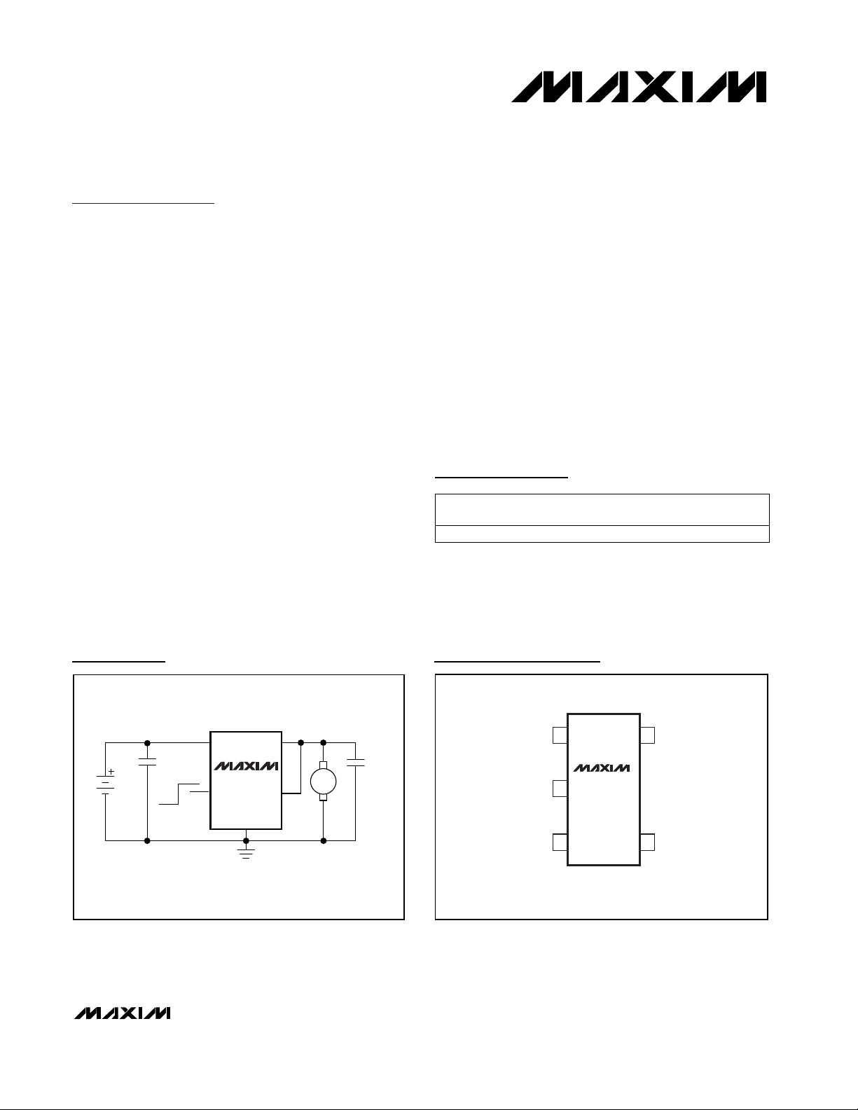
C
OUT
1µF
C
IN
1µF
BATTERY
1.25V
UP TO 120mA
2.5V TO 6.5V
ON
OFF
Typical Operating Circuit
19-1455; Rev 1; 6/99
PART
MAX1749EUK-T -40°C to +85°C
TEMP. RANGE
PIN-
PACKAGE
5 SOT23
Ordering Information
TOP
MARK
ADIX
For free samples & the latest literature: http://www.maxim-ic.com, or phone 1-800-998-8800.
For small orders, phone 1-800-835-8769.
TOP VIEW
GND
1
ON
2
3
IN
5
SET
MAX1749
OUT
4
SOT23-5
MAX1749
SOT23 Vibrator Motor Driver
2 _______________________________________________________________________________________
ABSOLUTE MAXIMUM RATINGS
ELECTRICAL CHARACTERISTICS
(VIN= +3.6V, TA= -40°C to +85°C, unless otherwise noted. Typical values are at TA= +25°C.) (Note 1)
Stresses beyond those listed under “Absolute Maximum Ratings” may cause permanent damage to the device. These are stress ratings only, and functional
operation of the device at these or any other conditions beyond those indicated in the operational sections of the specifications is not implied. Exposure to
absolute maximum rating conditions for extended periods may affect device reliability.
IN to GND ....................................................................-7V to +7V
Output Short-Circuit Duration ............................................Infinite
SET to GND ..............................................................-0.3V to +7V
ON to GND ..................................................................-7V to +7V
ON to IN....................................................................-7V to +0.3V
OUT to GND ................................................-0.3V to (V
IN
+ 0.3V)
Continuous Power Dissipation (T
A
= +70°C)
SOT23-5 (derate 7.1mW/°C above +70°C) .................571mW
Operating Temperature Range ...........................-40°C to +85°C
Junction Temperature......................................................+150°C
θ
JA
...............................................................................+140°C/W
Storage Temperature Range .............................-65°C to +150°C
Lead Temperature (soldering, 10sec) .............................+300°C
0.05
0 100
I
ON
ON Input Bias Current
V
0.4V
IL
ON Input High Threshold 2.0V
IH
V2.5 6.5V
IN
Input Voltage
µA80 200I
Q
Ground Pin Current
1.13 1.25 1.37 VV
OUT
Output Voltage
mA120Maximum Output Current
UNITSMIN TYP MAXSYMBOLPARAMETER
ON = IN
CONDITIONS
mA280I
LIM
Current Limit (Note 2)
0.1mA ≤ I
OUT
≤ 50mA, SET = OUT
Note 1: Limits are 100% production tested at T
A
= +25°C. Limits over the operating temperature range are guaranteed through cor-
relation using Statistical Quality Control (SQC) methods.
Note 2: Not tested. For design purposes, the current limit should be considered 120mA minimum to 420mA maximum.
TA= +85°C
TA= +25°C
nA
ON Input Low Threshold V
0.5TA= +85°C
TA= +25°C
nA
0.03 10
I
SET
SET Input Leakage Current V
SET
= 1.4V
°C170T
SHDN
Thermal Shutdown Temperature
°C20∆T
SHDN
Thermal Shutdown Hysteresis
µA
0.0001 1
I
OFF
Off Supply Current V
OUT
= VON= GND
0.02
ON INPUT
SET INPUT
THERMAL PROTECTION
TA= +85°C
TA= +25°C
MAX1749
SOT23 Vibrator Motor Driver
_______________________________________________________________________________________
3
)
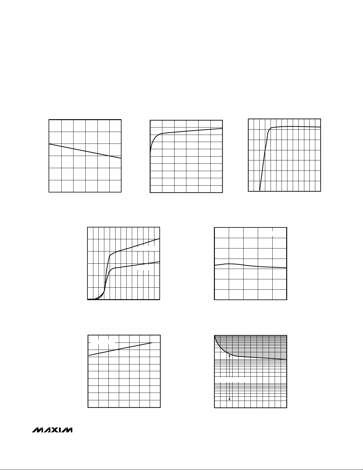
__________________________________________Typical Operating Characteristics
(V
IN
= +3.6V, SET = OUT, CIN= 1µF, C
OUT
= 1µF, TA= +25°C, unless otherwise noted.)
OUTPUT VOLTAGE
vs. LOAD CURRENT
1.27
1.26
1.25
1.24
1.23
OUTPUT VOLTAGE (V)
1.22
1.21
0406020 80 100 120
LOAD CURRENT (mA)
SUPPLY CURRENT vs. LOAD CURRENT
100
90
MAX1749 TOC01
80
70
60
50
40
30
SUPPLY CURRENT (µA)
20
10
0
04020 60 80 100 120
LOAD CURRENT (mA)
1.4
1.2
MAX1749toc02
1.0
0.8
0.6
OUTPUT VOLTAGE (V)
0.4
0.2
OUTPUT VOLTAGE
vs. INPUT VOLTAGE
0
0123456
INPUT VOLTAGE (V)
MAX1749toc03
SUPPLY CURRENT
vs. INPUT VOLTAGE
120
100
80
60
40
SUPPLY CURRENT (µA)
20
0
0123456
INPUT VOLTAGE (V)
SUPPLY CURRENT
vs. TEMPERATURE
100
I
= 50mA
LOAD
90
80
70
60
50
40
30
SUPPLY CURRENT (µA)
20
10
0
TEMPERATURE (°C
I
LOAD
I
LOAD
= 50mA
= 0
100806040200-20-40
MAX1749 toc04
MAX1749 toc06
OUTPUT VOLTAGE
vs. TEMPERATURE
1.28
1.27
1.26
1.25
1.24
OUTPUT VOLTAGE (V)
1.23
1.22
1.21
-40 10-15 35 60 85
TEMPERATURE (°C)
REGION OF STABLE C
vs. LOAD CURRENT
10
1
ESR (Ω)
OUT
C
STABLE REGION
0.1
0.01
0608020 40 100 120
LOAD CURRENT (mA)
I
LOAD
OUT
= 50mA
MAX1749 toc05
ESR
MAX1749 toc08

MAX1749
SOT23 Vibrator Motor Driver
4 _______________________________________________________________________________________
Typical Operating Characteristics (continued)
(V
IN
= +3.6V, SET = OUT, CIN= 1µF, C
OUT
= 1µF, TA= +25°C, unless otherwise noted.)
LINE-TRANSIENT RESPONSE
LOAD-TRANSIENT RESPONSE
1.25V
1.24V
1.23V
4.6V
3.6V
I
LOAD
5V
0V
1V
0V
200mA
0mA
50µs/div
= 50mA, C
= 10µF, V
IN
= AC-COUPLED
OUT
ON/OFF WAVEFORM (VIN = 5.0V)
MAX1749 toc09
V
OUT
V
IN
MAX1749 toc13
V
ON
V
OUT
I
LOAD
200mA
0mA
1.25V
1.24V
1.23V
I
= 0 to 50mA, C
LOAD
IN
ON/OFF WAVEFORM (VIN = 3.6V)
4V
2V
0V
1V
0V
10µs/div
= 10µF, V
= AC-COUPLED
OUT
MAX1749 toc10
V
OUT
I
LOAD
20mA/div
MAX1749 toc14
V
ON
V
OUT
I
LOAD
100ms/div
VIBRATOR MOTOR LOAD
VIBRATOR MOTOR LOAD
100ms/div

MAX1749
SOT23 Vibrator Motor Driver
_______________________________________________________________________________________ 5
Detailed Description
The MAX1749 is a low-quiescent-current, vibrator motor driver designed for battery-powered wireless handsets and
pagers. The device supplies an adjustable +1.25V to +6.5V
output for load currents up to 120mA. The MAX1749 allows
for a constant vibration force while operating from a +2.5V
to +6.5V input voltage range.
The 1.25V bandgap reference is connected to the error
amplifier’s inverting input. The error amplifier compares this
reference with the feedback voltage and amplifies the difference. The MOSFET driver reads the error signal and
applies the appropriate drive to the p-channel pass transistor. If the feedback voltage is lower than the reference voltage, the pass-transistor gate is pulled lower than the
reference, allowing more current to flow and increasing the
output voltage. If the feedback voltage is too high, the passtransistor gate is pulled-up, allowing less current to flow to
the output. The output voltage is fed back to SET either
directly for a 1.25V fixed output or through an external resistor-divider for an adjustable +1.25V to V
IN
output. Additional
blocks include a current limiter, reverse battery protection, a
thermal sensor, and ON/ OFF logic.
Internal P-Channel Pass Transistor
The MAX1749 features a 1.1Ω typical P-channel MOS-
FET pass transistor. This provides several advantages
over similar designs using PNP pass transistors, including longer battery life.
______________________________________________________________Pin Description
Active-High On/Off Input. Apply a logic high to deliver power to the load. Apply a logic low to disconnect the
load and reduce the supply current to 0.1nA.
ON1
PIN FUNCTIONNAME
GND2
Ground. This pin also functions as a heatsink. Solder to large pads or the circuit board ground plane to maximize thermal dissipation.
3
Regulator Input. Supply voltage can range from +2.5V to +6.5V. Bypass with 1µF to GND (see
Capacitor
Selection and Regulator Stability
).
OUT4
Regulator Output. Fixed 1.25V or adjustable from 1.25V to VIN. Sources up to 120mA. Bypass with a 1µF,
<0.2Ω typical ESR capacitor to GND.
IN
SET5
Feedback Input for Setting the Output Voltage. Connect to OUT for 1.25V regulated output (see
Output
Voltage Selection
). Connect to an external resistor-divider for adjustable-output operation.
Figure 1. Functional Diagram
IN
ON
REVERSE
BATTERY
PROTECTION
MAX1749
GND
ON/OFF
LOGIC
THERMAL
SENSOR
1.25V
REF
ERROR
AMP
MOS DRIVER
WITH I
LIMIT
P
OUT
SET

MAX1749
SOT23 Vibrator Motor Driver
6 _______________________________________________________________________________________
The P-channel MOSFET requires no base drive current,
which reduces quiescent current considerably. PNPbased regulators waste considerable amounts of base
current under large loads. The MAX1749 does not suffer from these problems and consumes only 80µA of
quiescent current independent of the load (see
Typical
Operating Characteristics
).
Output Voltage Selection
To select the preset 1.25V output, connect OUT directly
to SET. To adjust the output (1.25V to 6.5V), use two
external resistors connected as a voltage divider to SET
(Figure 2). The output voltage is set by the following
equation:
V
OUT
= V
SET
(1 + R1 / R2)
where V
SET
= 1.25V. To simplify resistor selection:
Choose R2 = 100kΩ to optimize power consumption,
accuracy, and high-frequency power-supply rejection.
The total current through the external resistive feedback
and load should not be less than 10µA.
ON/
OOFFFF
Drive ON high to provide power to the load. Drive ON
low to disable power to the load and reduce the supply
current to typically 0.1nA (1µA max). Refer to the
ON/OFF waveforms in the
Typical Operating Char-
acteristics
. When ON goes high, output current rises to
the current limit until V
OUT
reaches regulation. While in
regulation, the output current drops to a lower value
sufficient to maintain motor speed. When ON goes low,
the regulator turns off; however, inertial energy in the
motor exhibits a slow output voltage decline. The
MAX1749 is designed to withstand this condition with
no negative effects.
Current Limit
The MAX1749 includes a current limiter that monitors
and controls the pass transistor’s gate voltage, estimating the output current and limiting it to about 280mA.
For design purposes, the current limit should be considered 120mA (min) to 420mA (max). The output can
be shorted to ground for an infinite time period without
damaging the part.
Thermal-Overload Protection
Thermal-overload protection limits total power dissipation in the MAX1749. When the junction temperature
exceeds TJ= +170°C, the thermal sensor sends a signal to the ON/ OFF logic, turning off the pass transistor
and allowing the IC to cool. The thermal sensor will turn
the pass transistor on again after the IC’s junction temperature cools by typically 20°C, resulting in a pulsed
output during continuous thermal-overload conditions.
Operating Region and Power Dissipation
Maximum power dissipation of the MAX1749 depends
on the thermal resistance of the case and circuit board,
the temperature difference between the die junction
and ambient air, and the rate of air flow. The power dissipation across the device is P = I
OUT(VIN
- V
OUT
). The
resulting maximum power dissipation is:
P
MAX
= (TJ- T
A
) / θ
JA
where (TJ- TA) is the temperature difference between
the MAX1749 die junction and the surrounding air, and
θ
JA
is +140°C/W.
GND performs the dual function of providing an electrical connection to ground and channeling heat away.
Connect GND to a large pad or ground plane.
Reverse Battery Protection
The MAX1749 has a unique protection scheme that limits the reverse supply current to less than 1mA when
either VINor VONfalls below ground. The circuitry monitors the polarity of these two pins, disconnecting the
internal circuitry and parasitic diodes when the battery
is reversed. This feature prevents the device from overheating and damaging the battery.
VIN> 5.5V Minimum Load Current
When operating the MAX1749 with an input voltage
above 5.5V, the minimum current through the external
feedback resistors and load must be 30µA.
Figure 2. Adjustable Output Using External Feedback
Resistors
OUTPUT
BATTERY
C
1µF
MAX1749
GND
OUT
R1
SET
R2
IN
ON
IN
ON
OFF
C
1µF
OUT
VOLTAGE
VIBRATOR
R1 R2
=−
V
OUT
V
SET
1

MAX1749
SOT23 Vibrator Motor Driver
_______________________________________________________________________________________ 7
Capacitor Selection and
_________________Regulator Stability
Use a 1µF capacitor on the input and a 1µF capacitor
on the output of the MAX1749. A higher-value input
capacitor (10µF) may be necessary if large, fast transients are anticipated and the device is located several
inches from the power source. Improve load-transient
response and stability by using larger output capacitors. For stable operation over the full temperature
range with load currents up to 120mA, use a 1µF min
capacitor (ESR < 0.2Ω).
Chip Information
TRANSISTOR COUNT: 148
________________________________________________________Package Information
SOT5L.EPS

MAX1749
SOT23 Vibrator Motor Driver
Maxim cannot assume responsibility for use of any circuitry other than circuitry entirely embodied in a Maxim product. No circuit patent licenses are
implied. Maxim reserves the right to change the circuitry and specifications without notice at any time.
8
_____________________Maxim Integrated Products, 120 San Gabriel Drive, Sunnyvale, CA 94086 408-737-7600
© 1999 Maxim Integrated Products Printed USA is a registered trademark of Maxim Integrated Products.
NOTES
 Loading...