

Page 1
EVALUATION KIT AVAILABLE
19-6043; Rev 1; 3/12
MAX17498A/MAX17498B/MAX17498C
AC-DC and DC-DC Peak Current-Mode Converters
for Flyback/Boost Applications
General Description
The MAX17498A/MAX17498B/MAX17498C devices are
current-mode fixed-frequency flyback/boost converters
with a minimum number of external components. They
contain all the control circuitry required to design wide
input voltage isolated and nonisolated power supplies.
The MAX17498A has its rising/falling undervoltage lockout (UVLO) thresholds optimized for universal offline (85V
AC to 265V AC) applications, while the MAX17498B/
MAX17498C support UVLO thresholds suitable to lowvoltage DC-DC applications.
The switching frequency of the MAX17498A/MAX17498C
flyback converters is 250kHz, while that of the MAX17498B
flyback/boost converter is 500kHz. These frequencies
allow the use of tiny magnetic and filter components,
resulting in compact, cost-effective power supplies. An
EN/UVLO input allows the user to start the power supply
precisely at the desired input voltage, while also functioning as an on/off pin. The OVI pin enables implementation
of an input overvoltage-protection scheme that ensures
that the converter shuts down when the DC input voltage
exceeds the desired maximum value.
The devices incorporate a flexible error amplifier and an
accurate reference voltage (REF) to enable the end user to
regulate both positive and negative outputs. Programmable
current limit allows proper sizing and protection of the
primary switching FET. The MAX17498B supports a maximum duty cycle of 92% and provides programmable
slope compensation to allow optimization of control-loop
performance. The MAX17498A/MAX17498C support a
maximum duty cycle of 49%, and have fixed internal slope
compensation for optimum control-loop performance. The
devices provide an open-drain PGOOD pin that serves as a
power-good indicator and enters the high-impedance state
to indicate that the flyback/boost converter is in regulation. An SS pin allows programmable soft-start time for the
flyback/boost converter. Hiccup-mode overcurrent protection and thermal shutdown are provided to minimize
dissipation under overcurrent and overtemperature fault
conditions. The devices are available in a space-saving,
16-pin (3mm x 3mm) TQFN package with 0.5mm lead
spacing.
Ordering Information appears at end of data sheet.
Typical Application Circuits appears at end of data sheet.
Benefits and Features
S Peak Current-Mode Flyback/Boost Converter
S Current-Mode Control Provides Excellent
Transient Response
S Fixed Switching Frequency
250kHz (MAX17498A/MAX17498C)
500kHz (MAX17498B)
S Flexible Error Amplifier to Regulate Both Positive
and Negative Outputs
S Programmable Soft-Start to Reduce Input Inrush
Current
S Programmable Voltage or Current Soft-Start
S Power-Good Signal (PGOOD)
S Reduced Power Dissipation Under Fault
Hiccup-Mode Overcurrent Protection
Thermal Shutdown with Hysteresis
S Robust Protection Features
Flyback/Boost Programmable Current Limit
Input Overvoltage Protection
S Optimized Loop Performance
Programmable Slope Compensation for
Flyback /Boost Maximizes Obtainable Phase
Margin
S High Efficiency
175mI, 65V Rated n-Channel MOSFET Offers
Typical Efficiency Greater Than 80%
No Current-Sense Resistor
S Optional Spread Spectrum
S Space-Saving, 16-Pin (3mm x 3mm) TQFN
Package
Applications
Front-End AC-DC Power Supplies for Industrial
Applications (Isolated and Nonisolated)
Telecom Power Supplies
Wide Input Range DC Input Flyback/Boost
Industrial Power Supplies
For related parts and recommended products to use with this part,
refer to www.maxim-ic.com/MAX17498A.related.
_________________________________________________________________ Maxim Integrated Products 1
For pricing, delivery, and ordering information, please contact Maxim Direct at 1-888-629-4642,
or visit Maxim’s website at www.maxim-ic.com.
Page 2
MAX17498A/MAX17498B/MAX17498C
AC-DC and DC-DC Peak Current-Mode Converters
for Flyback/Boost Applications
ABSOLUTE MAXIMUM RATINGS
IN to SGND ............................................................-0.3V to +40V
EN/UVLO to SGND ......................................... -0.3V to IN + 0.3V
OVI to SGND .............................................. -0.3V to VCC + 0.3V
VCC to SGND .......................................................... -0.3V to +6V
SS, LIM, EA-, EA+, COMP, SLOPE,
REF to SGND ........................................ -0.3V to (VCC + 0.3V)
LX to SGND ........................................................... -0.3V to +70V
PGOOD to SGND .................................................... -0.3V to +6V
Stresses beyond those listed under “Absolute Maximum Ratings” may cause permanent damage to the device. These are stress ratings only, and functional operation of the device at these or any other conditions beyond those indicated in the operational sections of the specifications is not implied. Exposure to absolute
maximum rating conditions for extended periods may affect device reliability.
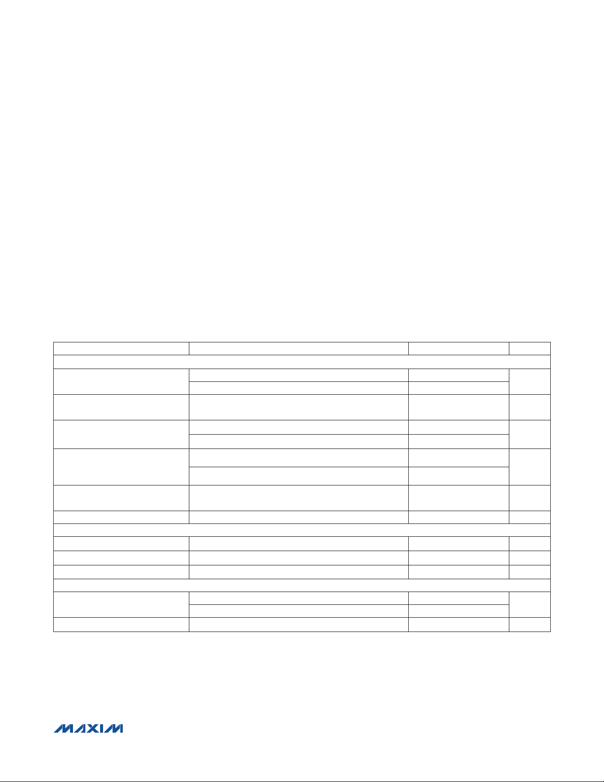
ELECTRICAL CHARACTERISTICS
(VIN = +15V, V
values are at TA = +25°C.) (Note 1)
INPUT SUPPLY (VIN)
IN Voltage Range (VIN)
IN Supply Startup Current Under
UVLO
IN Supply Current (IIN)
IN Boostrap UVLO Rising
Threshold
IN Bootstrap UVLO Falling
Threshold
IN Clamp Voltage EN/UVLO = SGND, IIN = 1mA (MAX17498A) (Note 2) 31 33.5 36 V
LINEAR REGULATOR (VCC)
VCC Output Voltage Range 6V < VIN < 29V, 0mA < I
VCC Dropout Voltage VIN = 4.5V, I
VCC Current Limit VCC = 0V, VIN = 6V 50 100 mA
ENABLE (EN/UVLO)
EN/UVLO Threshold
EN/UVLO Input Leakage Current
EN/UVLO
PARAMETER CONDITIONS MIN TYP MAX UNITS
= +2V, COMP = open, CIN = 1µF, C
MAX17498A 4.5 29
MAX17498B/MAX17498C 4.5 36
I
INSTARTUP
Switching, fSW = 250kHz (MAX17498A/MAX17498C) 1.8 3
Switching, fSW = 500kHz (MAX17498B) 2 3.25
MAX17498A 19 20.5 22
MAX17498B/MAX17498C 3.85 4.15 4.4
Rising 1.18 1.23 1.28
Falling 1.11 1.17 1.21
0V < V
, VIN < UVLO or EN/UVLO = SGND 22 36 µA
= 20mA 160 300 mV
VCC
EN/UVLO
< 1.5V, TA = +25NC
VCC
PGND to SGND .................................................... -0.3V to +0.3V
Continuous Power Dissipation (Single-Layer Board)
TQFN (derate 20.8mW/°C above +70°C)..................1700mW
Operating Temperature Range ........................ -40°C to +125°C
Storage Temperature Range ............................ -65°C to +160°C
Junction Temperature (continuous) ................................+150°C
Lead Temperature (soldering, 10s) ................................+300°C
Soldering Temperature (reflow) ......................................+260°C
= 1µF, TA = TJ = -40°C to +125°C, unless otherwise noted. Typical
V
mA
V
3.65 3.95 4.25 V
< 50mA 4.8 5 5.2 V
VCC
V
-100 0 +100 nA
_________________________________________________________________ Maxim Integrated Products 2
Page 3
MAX17498A/MAX17498B/MAX17498C
AC-DC and DC-DC Peak Current-Mode Converters
for Flyback/Boost Applications
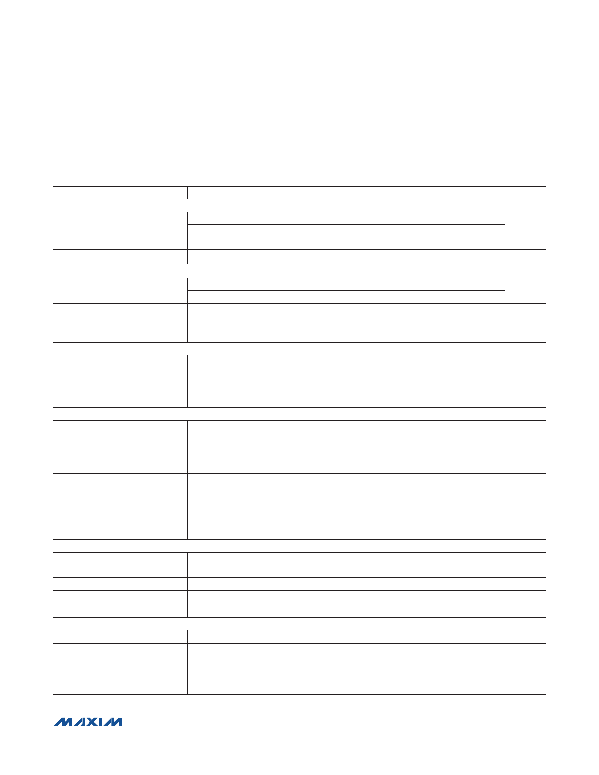
ELECTRICAL CHARACTERISTICS (continued)
(VIN = +15V, V
values are at TA = +25°C.) (Note 1)
OVERVOLTAGE PROTECTION (OVI)
OVI Threshold
OVI Masking Delay 2 µs
OVI Input Leakage Current
SWITCHING FREQUENCY AND MAXIMUM DUTY CYCLE (f
Switching Frequency
Maximum Duty Cycle
Minimum Controllable On Time t
SOFT-START (SS)
SS Set-Point Voltage 1.2 1.22 1.24 V
SS Pullup Current VSS = 400mV 9 10 11 µA
SS Peak Current-Limit-Enable
Threshold
ERROR AMPLIFIER (EA+, EA-, and COMP)
EA+ Input Bias Current
EA- Input Bias Current
Error-Amplifier Open-Loop
Voltage Gain
Error-Amplifier
Transconductance
Error-Amplifier Source Current V
Error-Amplifier Sink Current V
Current-Sense Transresistance 0.45 0.5 0.55
INTERNAL SWITCH
DMOS Switch On-Resistance
(R
DSON
DMOS Peak Current Limit LIM = 100K 1.62 1.9 2.23 A
DMOS Runaway Current Limit LIM = 100K 1.9 2.3 2.6 A
LX Leakage Current
CURRENT LIMIT (LIM)
LIM Reference Current 9 10 11 µA
Peak Switch Current Limit with
LIM Open
Runaway Switch Current Limit
with LIM Open
EN/UVLO
PARAMETER CONDITIONS MIN TYP MAX UNITS
)
= +2V, COMP = open, CIN = 1µF, C
Rising 1.18 1.23 1.28
Falling 1.11 1.17 1.21
0V < V
MAX17498A/MAX17498C 235 250 265
MAX17498B 470 500 530
MAX17498A/MAX17498C 47.5 48.75 50
MAX17498B 90 92 94
ONMIN
V
EA+
V
EA-
V
COMP
COMP
COMP
I
LX
VLX = 65V, TA = +25NC
< 1.5V, TA = +25NC
OVI
= 1.5V, TA = +25NC
= 1.5V, TA = +25NC
= 2V, V
= 2V, EA- < EA+ 80 120 210 µA
= 2V, EA- > EA+ 80 120 210 µA
= 200mA 175 380
= 1V 1.5 1.8 2.1 mS
LIM
= 1µF, TA = TJ = -40°C to +125°C, unless otherwise noted. Typical
VCC
-100 0 +100 nA
SW and DMAX
)
110 ns
1.11 1.17 1.21 V
-100 +100 nA
-100 +100 nA
90 dB
0.1 1 µA
0.39 0.45 0.54 A
0.39 0.5 0.6 A
V
kHz
%
I
mI
_________________________________________________________________ Maxim Integrated Products 3
Page 4
MAX17498A/MAX17498B/MAX17498C
AC-DC and DC-DC Peak Current-Mode Converters
for Flyback/Boost Applications
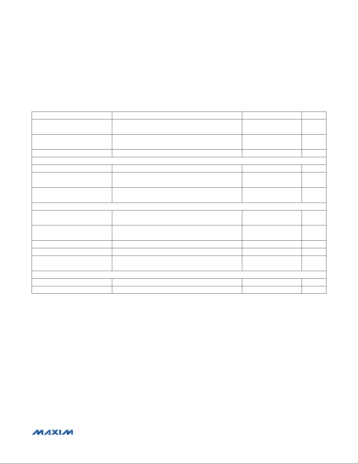
ELECTRICAL CHARACTERISTICS (continued)
(VIN = +15V, V
values are at TA = +25°C.) (Note 1)
Number of Peak Current-Limit
Hits Before Hiccup Timeout
Number of Runaway CurrentLimit Hits Before Hiccup Timeout
Overcurrent Hiccup Timeout 32 ms
SLOPE COMPENSATION (SLOPE)
SLOPE Pullup Current 9 10 11 µA
SLOPE-Compensation Resistor
Range
Default SLOPE-Compensation
Ramp
POWER-GOOD SIGNAL (PGOOD)
PGOOD Output-Leakage
Current (Off State)
PGOOD Output Voltage
(On State)
PGOOD Higher Threshold EA- rising 93.5 95 96.5 %
PGOOD Lower Threshold EA- falling 90.5 92 93.5 %
PGOOD Delay After
EA- Reaches 95% Regulation
THERMAL SHUTDOWN
Thermal-Shutdown Threshold Temperature rising +160
Thermal-Shutdown Hysteresis 20
Note 1: All devices are 100% production tested at TA = +25NC. Limits over temperature are guaranteed by design.
Note 2: The MAX17498A is intended for use in universal input power supplies. The internal clamp circuit at IN is used to prevent the
EN/UVLO
PARAMETER CONDITIONS MIN TYP MAX UNITS
bootstrap capacitor from changing to a voltage beyond the absolute maximum rating of the device when EN/UVLO is low
(shutdown mode). Externally limit the maximum current to IN (hence to clamp) to 2mA (max) when EN/UVLO is low.
= +2V, COMP = open, CIN = 1µF, C
MAX17498B 30 150
SLOPE = open 60 mV/µs
V
PGOOD
I
PGOOD
= 5V, TA = +25NC
= 10mA 0 0.4 V
= 1µF, TA = TJ = -40°C to +125°C, unless otherwise noted. Typical
VCC
8 #
1 #
-1 +1 µA
4 ms
kI
NC
NC
_________________________________________________________________ Maxim Integrated Products 4
Page 5
MAX17498A/MAX17498B/MAX17498C
AC-DC and DC-DC Peak Current-Mode Converters
for Flyback/Boost Applications
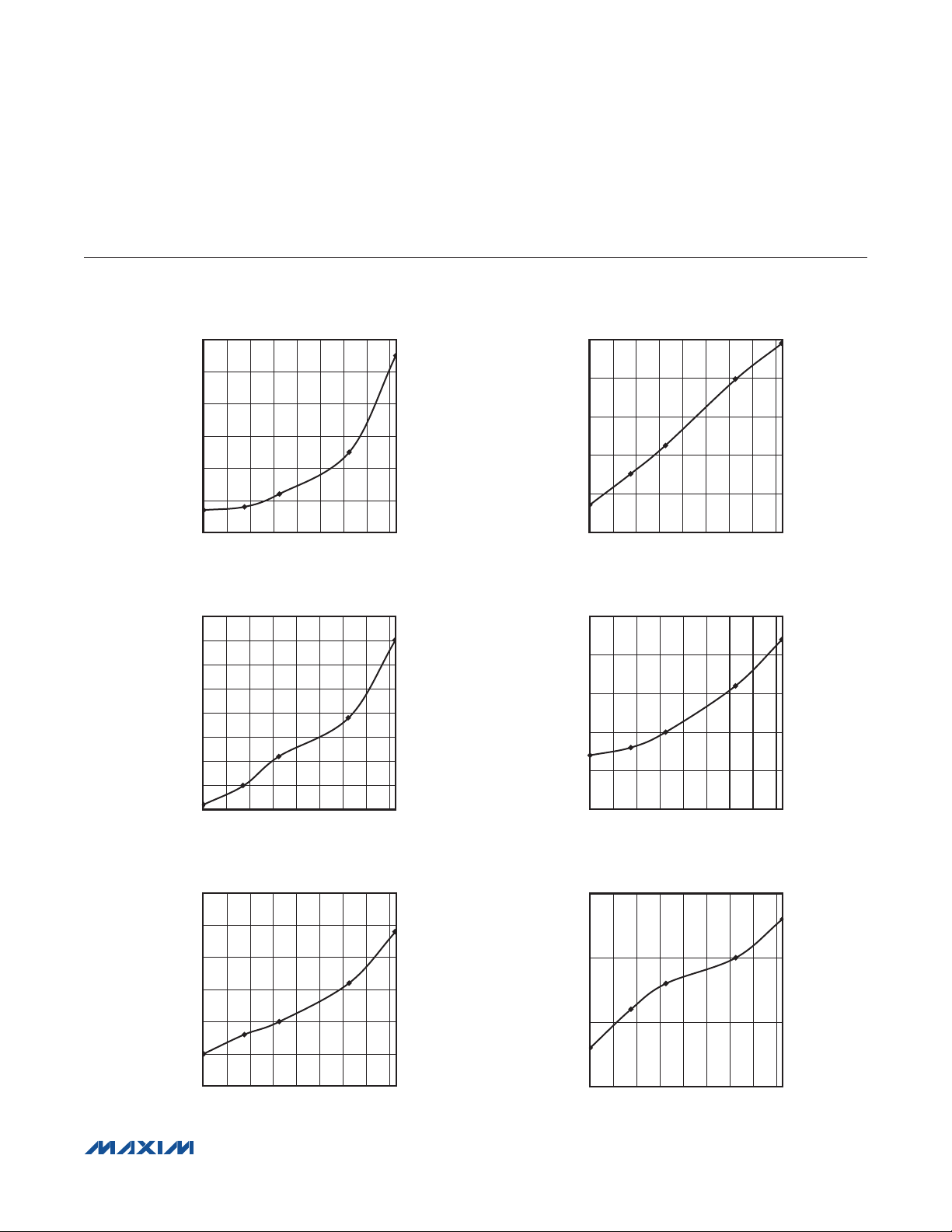
Typical Operating Characteristics
(VIN = +15V, V
EN/UVLO
= +2V, COMP = open, CIN = 1µF, C
BOOTSTRAP UVLO WAKE-UP LEVEL
vs. TEMPERATURE (MAX17498A)
20.26
20.24
20.22
20.20
20.18
20.16
BOOTSTRAP UVLO WAKE-UP LEVEL (V)
20.14
-40
TEMPERATURE (°C)
IN UVLO SHUTDOWN LEVEL
vs. TEMPERATURE
4.015
4.010
4.005
4.000
3.995
3.990
3.985
IN UVLO SHUTDOWN LEVEL (V)
3.980
3.975
-40
TEMPERATURE (°C)
EN/ UVLO FALLING LEVEL
vs. TEMPERATURE
1.170
120100806040200-20
120100-20 0206040 80
MAX17498 toc01
MAX17498 toc03
= 1µF, TA = TJ = -40°C to +125°C, unless otherwise noted.)
VCC
IN UVLO WAKE-UP LEVEL vs. TEMPERATURE
(MAX17498B/MAX17498C)
4.15
4.10
4.05
4.00
IN UVLO WAKE-UP LEVEL (V)
3.95
3.90
TEMPERATURE (°C)
EN/UVLO RISING LEVEL
vs. TEMPERATURE
1.235
1.230
1.225
1.220
EN/UVLO RISING LEVEL (V)
1.215
1.210
TEMPERATURE (°C)
OVI RISING LEVEL
vs. TEMPERATURE
1.225
MAX17498 toc02
120100806040200-20-40
MAX17498 toc04
120100806040200-20-40
1.165
1.160
1.155
1.150
EN/UVLO FALLING LEVEL (V)
1.145
1.140
-40
TEMPERATURE (°C)
120100806040200-20
MAX17498 toc05
1.220
1.215
OVI RISING LEVEL (V)
1.210
-40
120100806040200-20
TEMPERATURE (°C)
_________________________________________________________________ Maxim Integrated Products 5
MAX17498 toc06
Page 6
MAX17498A/MAX17498B/MAX17498C
AC-DC and DC-DC Peak Current-Mode Converters
for Flyback/Boost Applications
Typical Operating Characteristics (continued)
(VIN = +15V, V
EN/UVLO
1.160
1.155
1.150
1.145
OVI FALLING LEVEL (V)
1.140
1.135
= +2V, COMP = open, CIN = 1µF, C
IN CURRENT DURING SWITCHING
2.6
2.4
2.2
2.0
OVI FALLING LEVEL
vs. TEMPERATURE
TEMPERATURE (°C)
vs. TEMPERATURE
120100806040200-20-40
MAX17498 toc07
MAX17498 toc09
= 1µF, TA = TJ = -40°C to +125°C, unless otherwise noted.)
VCC
IN CURRENT UNDER UVLO
vs. TEMPERATURE
30
28
26
24
IN CURRENT UNDER UVLO (µA)
22
20
TEMPERATURE (°C)
LX AND PRIMARY CURRENT WAVEFORM
MAX17498 toc10
120100806040200-20-40
MAX17498 toc08
V
LX
20V/div
1.8
1.6
IN CURRENT DURING SWITCHING (mA)
1.4
-40
TEMPERATURE (°C)
EN STARTUP WAVEFORM
400µs/div
MAX17498 toc11
120100806040200-20
EN/UVLO
5V/div
V
OUT
5V/div
V
COMP
1V/div
1µs/div
EN SHUTDOWN WAVEFORM
400µs/div
MAX17498 toc12
_________________________________________________________________ Maxim Integrated Products 6
I
PRI
0.5A/div
EN/UVLO
5V/div
V
OUT
5V/div
V
COMP
1V/div
Page 7
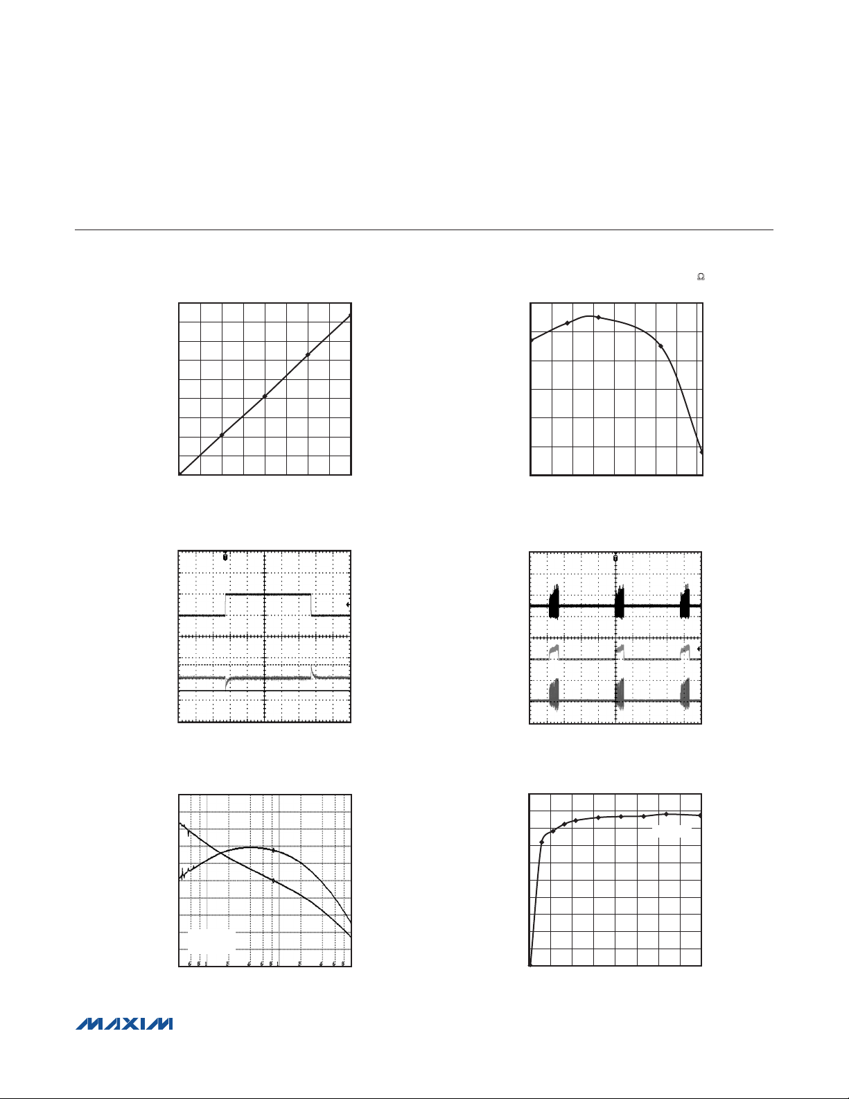
MAX17498A/MAX17498B/MAX17498C
08
AC-DC and DC-DC Peak Current-Mode Converters
for Flyback/Boost Applications
Typical Operating Characteristics (continued)
(VIN = +15V, V
EN/UVLO
= +2V, COMP = open, CIN = 1µF, C
PEAK CURRENT LIMIT (I
AT ROOM TEMPERATURE
vs. R
1800
1600
1400
1200
1000
800
600
PEAK CURRENT LIMIT (mA)
400
200
0
LIM
R
AT ROOM TEMPERATURE (kI)
LIM
TRANSIENT RESPONSE FOR 50%
LOAD STEP ON FLYBACK OUTPUT (5V)
)
LIM
706040 5020 3010
MAX17498 toc15
MAX17498 toc13
0
I
LOAD
500mA/div
= 1µF, TA = TJ = -40°C to +125°C, unless otherwise noted.)
VCC
PEAK CURRENT LIMIT AT R
= 100kI
LIM
vs. TEMPERATURE
2.00
1.99
(A)
LIM
1.98
1.97
1.96
PEAK CURRENT LIMIT AT R
1.95
1.94
-40
TEMPERATURE AT GIVEN R
SHORT-CIRCUIT PROTECTION
LIM
(°C)
MAX17498 toc16
120100806040200-20
MAX17498 toc14
V
LX
50V/div
V
OUT
500mV/div
I
PRI
2A/div
2ms/div
V
OUT
200mV/div
10ms/div
EFFICIENCY GRAPH AT 24V INPUT
BODE PLOT - (5V OUTPUT AT 24V INPUT)
BW = 8.3kHz
PM = 63°
LOG (F)
MAX17498 toc17
PHASE
36°/div
GAIN
10dB/div
100
90
80
70
60
50
40
EFFICIENCY (%)
30
20
10
0
(FLYBACK REGULATOR)
VIN = 24V
LOAD CURRENT (A)
MAX17498 toc18
1.41.20.8 1.00.4 0.60.20
_________________________________________________________________ Maxim Integrated Products 7
Page 8
MAX17498A/MAX17498B/MAX17498C
AC-DC and DC-DC Peak Current-Mode Converters
for Flyback/Boost Applications
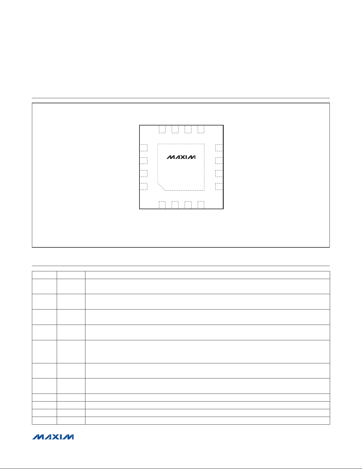
Pin Configuration
TOP VIEW
PGOOD
PGND
13
14
LX
15
16
IN
+
REF
N.C.
12 11 9
12
EN/UVLO
10
MAX17498A
MAX17498B
MAX17498C
EP (SGND)
3
CC
V
TQFN-EP
OVI N.C.
EA+
SS
8
7
COMP
EA-
6
SLOPE
5
4
LIM
Pin Description
PIN NAME FUNCTION
1 EN/UVLO
2 V
CC
3 OVI
4 LIM
5 SLOPE
6 EA-
7 COMP
8 SS Soft-Start Pin. Connect a capacitor from SS to SGND to set the soft-start time interval.
9 EA+ Noninverting Input of the Flexible Error Amplifier. Connect to SS to use 1.22V as the reference.
10, 12 N.C. No Connection
11 REF Internal 1.22V Reference Output Pin. Connect a 100pF capacitor from REF to SGND.
Enable/Undervoltage-Lockout Pin. Drive to > 1.23V to start the devices. To externally program the UVLO
threshold of the input supply, connect a resistor-divider between input supply EN/UVLO and SGND.
Linear Regulator Output. Connect input bypass capacitor of at least 1µF from VCC to SGND as close as
possible to the IC.
Overvoltage Comparator Input. Connect a resistor-divider between the input supply (OVI) and SGND to
set the input overvoltage threshold.
Current-Limit Setting Pin. Connect a resistor between LIM and SGND to set the peak-current limit for
nonisolated flyback converter. Peak-current limit defaults to 500mA if unconnected.
Slope Compensation Input Pin. Connect a resistor between SLOPE and SGND to set slopecompensation ramp. Connect to VCC for minimum slope compensation. See the Programming Slope
Compensation (SLOPE) section.
Inverting Input of the Flexible Error Amplifier. Connect to mid-point of resistor-divider from the positive
terminal output to SGND.
Flexible Error-Amplifier Output. Connect the frequency-compensation network between COMP and
SGND.
_________________________________________________________________ Maxim Integrated Products 8
Page 9
MAX17498A/MAX17498B/MAX17498C
AC-DC and DC-DC Peak Current-Mode Converters
for Flyback/Boost Applications
Pin Description (continued)
PIN NAME FUNCTION
13 PGOOD
14 PGND Power Ground for Converter
15 LX External Transformer/Inductor Connection for the Converter
16 IN
—
EP
(SGND)
Open-Drain Output. PGOOD goes high when EA- is within 5% of the set point. PGOOD pulls low when
EA- falls below 92% of its set-point value.
Internal Linear Regulator Input. Connect IN to the input-voltage source. Bypass IN to PGND with a 1µF
(min) ceramic capacitor.
Exposed Pad. Internally connected to SGND. Connect EP to a large copper plane at SGND potential to
provide adequate thermal dissipation. Connect EP (SGND) to PGND at a single point.
Detailed Description
The MAX17498A offers a bootstrap UVLO wakeup level
of 20V with a wide hysteresis of 15V (min) optimized
for implementing an isolated and nonisolated universal
(85V AC to 265V AC) offline single-switch flyback
converter or telecom (36V to 72V) power supplies. The
MAX17498B/MAX17498C offer a UVLO wakeup level of
4.4V and are well suited for low-voltage DC-DC flyback/
boost power supplies. An internal reference (1.22V)
can be used to regulate the output down to 1.23V in
nonisolated flyback and boost applications. Additional
semi-regulated outputs, if needed, can be generated
by using additional secondary windings on the flyback
converter transformer. A flexible error amplifier and REF
allow the end-user selection between regulating positive
and negative outputs.
The devices utilize peak current-mode control and external compensation for optimizing the loop performance for
various inductors and capacitors. The devices include a
cycle-by-cycle peak current limit and eight consecutive
occurrences of current-limit event trigger hiccup mode,
that protect external components by halting switching for
a period of time (32ms). The devices also include voltage
soft-start for nonisolated designs and current soft-start
for isolated designs to allow monotonic rise of the output
voltage. The voltage or current soft-start can be selected
using the SLOPE pin. See the Block Diagram for more
information.
Input Voltage Range
The MAX17498A has different rising and falling UVLO
thresholds on the IN pin than those of the MAX17498B/
MAX17498C. The thresholds for the MAX17498A are
optimized for implementing power-supply startup
schemes typically used for offline AC-DC power supplies.
The MAX17498A is therefore well suited for operation from the rectified DC bus in AC-DC power-supply
applications typically encountered in front-end industrial
power-supply applications. As such, the MAX17498A
has no limitation on the maximum input voltage as long
as the external components are rated suitably and the
maximum operating voltages of the MAX17498A are
respected. The MAX17498A can successfully be used
in universal input-rectified (85V to 265V AC) bus applications, rectified 3-phase DC bus applications, and telecom (36V to 72V DC) applications.
The MAX17498B/MAX17498C are intended for implementing a flyback (isolated and nonisolated) and
boost converter with an on-board 65V rated n-channel
MOSFET. The IN pin of the MAX17498B/MAX17498C has
a maximum operating voltage of 36V. The MAX17498B/
MAX17498C implement rising and falling thresholds on
the IN pin that assume power-supply startup schemes,
typical of lower voltage DC-DC applications, down to an
input voltage of 4.5V DC. Therefore, flyback converters
with a 4.5V to 36V supply voltage range can be implemented with the MAX17498B/MAX17498C.
Internal Linear Regulator (VCC)
The internal functions and driver circuits are designed
to operate from a 5V Q5% power-supply voltage. The
devices have an internal linear regulator that is powered
from the IN pin and generates a 5V power rail. The output
of the linear regulator is connected to the VCC pin and
should be decoupled with a 2.2µF capacitor to ground
for stable operation. The VCC converter output supplies
the operating current for the devices. The maximum
operating voltage of the IN pin is 29V for the MAX17498A
and 36V for the MAX17498B/MAX17498C.
_________________________________________________________________ Maxim Integrated Products 9
Page 10

MAX17498A/MAX17498B/MAX17498C
AC-DC and DC-DC Peak Current-Mode Converters
for Flyback/Boost Applications
Configuring the Power Stage (LX)
The devices use an internal n-channel MOSFET to implement internal current sensing for current-mode control
and overcurrent protection of the flyback/boost converter. To facilitate this, the drain of the internal nMOSFET is
connected to the source of the external MOSFET in the
MAX17498A high-input-voltage applications. The gate of
the external MOSFET is connected to the IN pin. Ensure
by design that the IN pin voltage does not exceed the
maximum operating gate-voltage rating of the external
MOSFET. The external MOSFET gate-source voltage is
controlled by the switching action of the internal nMOSFET, while also sensing the source current of the external MOSFET. In the MAX17498B/MAX17498C-based
applications, the LX pin is directly connected to either
the flyback transformer primary winding or to the boostconverter inductor.
IN REF
V
EN/UVLO
OVI
CC
5V, 50mA
1.23V
POK
LDO
33V CLAMP
(MAX17498A ONLY)
BG
CHIPEN
V
CS
Maximum Duty Cycle
The MAX17498A/MAX17498C operate at a maximum
duty cycle of 49%. The MAX17498B offers a maximum
duty cycle of 92% to implement both flyback and boost
converters involving large input-to-output voltage ratios
in DC-DC applications.
Power-Good Signal (PGOOD)
The devices include a PGOOD signal that serves as
a power-good signal to the system. PGOOD is an
open-drain signal and requires a pullup resistor to the
preferred supply voltage. The PGOOD signal monitors
EA- and pulls high when EA- is 95% (typ) of its regulation
value (1.22V). For isolated power supplies, PGOOD cannot serve as a power-good signal.
CHIPEN
HICCUP
CLK
10µA
1.17V
V
SUM
V
SLOPE
SSDONEF
V
CS
MAX17498A
MAX17498B
MAX17498C
OSC
SS
LX
1.23V
LIM
SLOPE
10µA
10µA
1.23V
250mV
DECODER
VOLTAGE SS CURRENT SS
LIMINT
V
SUM
COMP
FIXED SLOPE
VARIABLE SLOPE
Figure 1. MAX17498A/MAX17498B/MAX17498C Block Diagram
________________________________________________________________ Maxim Integrated Products 10
RUNAWAY
PEAK
PWM
CONTROL
LOGIC AND
DRIVER
CHIPEN
EA-
8 PEAK OR 1
RUNAWAY
PGOOD
BLOCK
SSDONE
PGND
PGOOD
COMP
EA+
EA-
Page 11

MAX17498A/MAX17498B/MAX17498C
AC-DC and DC-DC Peak Current-Mode Converters
for Flyback/Boost Applications
Soft-Start
The devices implement soft-start operation for the
flyback /boost converter. A capacitor connected to the
SS pin programs the soft-start period for the flyback/
boost converter. The soft-start feature reduces the input
inrush current. These devices allow the end user to select
between voltage soft-start usually preferred in nonisolated applications and current soft-start, which is useful in
isolated applications to get a monotonic rise in the output
voltage. See the Programming Soft-Start of the Flyback/
Boost Converter (SS) section.
Spread-Spectrum Factory Option
For EMI-sensitive applications, a spread-spectrumenabled version of the device can be requested from
the factory. The frequency-dithering feature modulates
the switching frequency by Q10% at a rate of 4kHz.
This spread-spectrum-modulation technique spreads
the energy of switching-frequency harmonics over a
wider band while reducing their peaks, helping to meet
stringent EMI goals.
Applications Information
Startup Voltage and Input Overvoltage-
Protection Setting (EN/UVLO, OVI)
The devices’ EN / UVLO pin serves as an enable /disable
input, as well as an accurate programmable input UVLO
pin. The devices do not commence startup operation
unless the EN/UVLO pin voltage exceeds 1.23V (typ).
The devices turn off if the EN/UVLO pin voltage falls
below 1.17V (typ). A resistor-divider from the input DC
bus to ground can be used to divide down and apply a
fraction of the input DC voltage (VDC) to the EN/UVLO
pin. The values of the resistor-divider can be selected
so that the EN/UVLO pin voltage exceeds the 1.23V (typ)
turn-on threshold at the desired input DC bus voltage. The
same resistor-divider can be modified with an additional
resistor (R
in
addition to the EN/UVLO functionality as shown in
Figure 2. When voltage at the OVI pin exceeds 1.23V (typ),
the devices stop switching and resume switching operations
only if voltage at the OVI pin falls below 1.17V (typ).
For given values of startup DC input voltage (V
) to implement input overvoltage protection
OVI
START
),
and input overvoltage-protection voltage (V
resistor values for the divider can be calculated as follows, assuming a 24.9kI resistor for R
V
R R 1k
= × −Ω
EN OVI
where R
where REN and R
applications, R
is in kI while V
OVI
= + × −Ω
R R R 1k
SUM OVI EN
are in kI. In universal AC input
OVI
might need to be implemented as
SUM
equal resistors in series (R
OVI
V
START
and V
START
V
START
1.23
, R
DC1
DC2
:
OVI
are in volts.
OVI
, R
DC3
voltage across each resistor is limited to its maximum
operation voltage.
R
RRR k
= = = Ω
DC1 DC1 D C1
SUM
3
For low-voltage DC-DC applications based on the
MAX17498B/MAX17498C, a single resistor can be used
in the place of R
, as the voltage across it is
SUM
approximately 40V.
V
DC
R
DC1
R
R
SUM
DC2
R
DC3
EN/UVLO
R
EN
OVI
R
OVI
MAX17498A
MAX17498B
MAX17498C
), the
OVI
) so that
Figure 2. Programming EN/UVLO and OVI
________________________________________________________________ Maxim Integrated Products 11
Page 12

MAX17498A/MAX17498B/MAX17498C
=+×
Rk
AC-DC and DC-DC Peak Current-Mode Converters
for Flyback/Boost Applications
Startup Operation
The MAX17498A is optimized for implementing an offline
single-switch flyback converter and has a 20V IN UVLO
wake-up level with hysteresis of 15V (min). In offline applications, a simple cost-effective RC startup circuit is used.
When the input DC voltage is applied, the startup resistor (R
causing the voltage at the IN pin to increase
) charges the startup capacitor (C
START
),
START
towards the
wake-up IN UVLO threshold (20V typ). During this time,
the MAX17498A draws a low startup
through R
. When the voltage at IN reaches the
START
current of 20µA (typ)
wake-up IN UVLO threshold, the MAX17498A commences switching operations and drives the internal n-channel
MOSFET whose drain is connected to the LX pin. In this
condition, the MAX17998A draws 1.8mA current from
C
, in addition to the current required to switch the
START
gate of the external nMOSFET. Since this current cannot
be supported by the current through R
age on C
starts to drop. When suitably configured,
START
START
, the volt-
as shown in Figure 10, the external nMOSFET is
switched by the LX pin and the flyback/forward converter generates an output voltage (V
to the IN pin through the diode (D2). If V
) bootstrapped
OUT
OUT
exceeds
the sum of 5V and the drop across D2 before the voltage on C
sustained by V
operating with energy from V
falls below 5V, then the IN voltage is
START
, allowing the MAX17498A to continue
OUT
. The large hysteresis
OUT
(15V typ) of the MAX17498A allows for a small startup
capacitor (C
allows the use of a large start resistor (R
). The low startup curent (20µA typ)
START
), thus reducing
START
power dissipation at higher DC bus voltages. Figure 3 shows
the typical RC startup scheme for the MAX17498A.
R
resistors in series (R
might need to be implemented as equal, multiple
START
V
DC
R
IN1
IN1
, R
IN2
, and R
) to share the
IN3
V
DC
V
OUT
D1
C
OUT
applied high DC voltage in offline applications so that
the voltage across each resistor is limited to the maximum
continuous operating-voltage rating. R
START
and C
START
can be calculated as:
C I µF
START IN
Q ft
×
GATE sw SS
10
6
10
where IIN is the supply current drawn at the IN pin
in mA, Q
is the gate charge of the external
GATE
nMOSFET used in nC, fSW is the switching frequency
of the converter in Hz, and tSS is the soft-start time
programmed for the flyback/forward converter in ms.
See the Programming Soft-Start of the Flyback/Boost
Converter (SS) section.
where C
V 10 50
( )
START
START
= Ω
is the startup capacitor in µF.
−×
START
1C
+
START
For designs that cannot accept power dissipation in the
startup resistors at high DC input voltages in offline applications, the startup circuit can be set up with a current
source instead of a startup resistor as shown in Figure 4.
V
DC
R
R
START
IN1
R
IN2
R
IN3
IN
V
DC
V
OUT
D1
C
OUT
R
R
START
IN2
V
V
OUT
R
C
D2
START
IN3
C
VCC
MAX17498A
IN
V
CC
LDO
LX
OUT
C
START
R
ISRC
D2
C
VCC
IN
V
CC
MAX17498A
LX
LDO
Figure 3. MAX17498A RC-Based Startup Circuit Figure 4. MAX17498A Current Source-Based Startup Circuit
________________________________________________________________ Maxim Integrated Products 12
Page 13

MAX17498A/MAX17498B/MAX17498C
=+×
AC-DC and DC-DC Peak Current-Mode Converters
for Flyback/Boost Applications
V
DC
IN
C
Figure 5. MAX17498B/MAX17498C Typical Startup Circuit with
IN Connected Directly to DC Input
R
Z
Z
D1
6.3V
Figure 6. MAX17498B/MAX17498C Typical Startup Circuit with
Bias Winding to Turn Off Q1 and Reduce Power Dissipation
IN
LDO
IN
MAX17498B
MAX17498C
Q1
IN
C
IN
C
VCC
IN
V
CC
The startup capacitor (C
C I µF
START IN
V
CC
C
VCC
LX Np Ns
V
DC
D2
NB
MAX17498B
MAX17498C
LDO
START
Qft
GATE SW SS
LX Np
) can be calculated as:
×
6
10
10
V
OUT
D1
C
OUT
V
OUT
D1
C
OUT
Ns
where IIN is the supply current drawn at the IN pin in mA,
Q
is the gate charge of the external MOSFET used
GATE
in nC, fSW is the switching frequency of the converter in
kHz, and tSS is the soft-start time programmed for the
flyback converter in ms.
Resistors R
and R
SUM
RM
SUM
RM
can be calculated as:
ISRC
V
START
= Ω
10
V
BEQ1
= Ω
ISRC
70
The IN UVLO wakeup threshold of the MAX17498B/
MAX17498C is set to 3.9V (typ) with a 200mV hysteresis, optimized for low-voltage DC-DC applications
down to 4.5V. For applications where the input DC
voltage is low enough (e.g., 4.5V to 5.5V DC) that the
power loss incurred to supply the operating current of
the MAX17498B/MAX17498C can be tolerated, the IN
pin is directly connected to the DC input, as shown in
Figure 5. In the case of higher DC input voltages (e.g., 16V
to 32V DC), a startup circuit, such as that shown in Figure 6,
can be used to minimize power dissipation in the startup
circuit. In this startup scheme, the transistor (Q1)
supplies the switching current until a bias winding NB
comes up. The resistor (RZ) can be calculated as:
R 9 (V 6.3) k=× −Ω
Z INMIN
where V
is the minimum input DC voltage.
INMIN
Programming Soft-Start of the
Flyback/Boost Converter (SS)
The soft-start period in the voltage soft-start scheme of
the devices can be programmed by selecting the value
of the capacitor connected from the SS pin to GND.
The capacitor CSS can be calculated as:
C 8.13 t nF= ×
SS SS
where tSS is expressed in ms.
The soft-start period in the current soft-start scheme
depends on the load at the output and the soft-start
capacitor.
Programming Output Voltage
The devices incorporate a flexible error amplifier that
allows regulating to both the positive and negative
outputs. The positive output voltage of the converter
can be programmed by selecting the correct values
for the resistor-divider connected from V
OUT
, the flyback /boost output to ground, with the midpoint of the
divider connected to the EA- pin (Figure 7). With RB
selected in the range of 20kI to 50kI, RU can be
calculated as:
V
R R 1k
= × −Ω
UB
OUT
1.22
where RB is in kI.
________________________________________________________________ Maxim Integrated Products 13
Page 14

MAX17498A/MAX17498B/MAX17498C
AC-DC and DC-DC Peak Current-Mode Converters
for Flyback/Boost Applications
The negative output voltage of the converter can be
programmed by selecting the correct values for the
resistor-divider connected from V
, the flyback /boost
OUT
output to REF with the midpoint of the divider connected
to the EA+ pin (Figure 8). With R1 selected in the range
of 20kI to 50kI, R2 can be calculated as:
V
R2 R1 k
=×Ω
OUT
1.22
where R1 is in kI.
Current-Limit Programming (LIM)
The devices include a robust overcurrent-protection
scheme that protects the device under overload and
short-circuit conditions. For the flyback/boost converter, the devices include a cycle-by-cycle peak
current limit that turns off the driver whenever the
current into the LX pin exceeds an internal limit that is
programmed by the resistor connected from the LIM
pin to GND. The devices include a runaway current limit
that protects the device under high-input-voltage shortcircuit conditions when there is insufficient output voltage
available to restore the inductor current built up during the on period of the flyback/boost converter. Either
eight consecutive occurrences of the peak currentlimit event or one occurrence of the runaway current limit
trigger a hiccup mode that protects the converter by
immediately suspending switching for a period of time
(t
RSTART
). This allows the overload current to decay due
to power loss in the converter resistances, load, and
the output diode of the flyback/boost converter before
soft-start is attempted again. The resistor at the LIM pin
for a desired current limit (IPK) can be calculated as:
R 50 I k=×Ω
LIM PK
where IPK is expressed in amperes.
For a given peak current-limit setting, the runaway
current limit is typically 20% higher. The peak currentlimit-triggered hiccup operation is disabled until the end
of soft-start, while the runaway current-limit-triggered hiccup operation is always enabled.
Programming Slope Compensation (SLOPE)
Since the MAX17498A/MAX17498C operate at a maximum duty cycle of 49%, in theory they do not require slope
compensation for preventing subharmonic instability that
occurs naturally in continuous-mode peak current-modecontrolled converters operating at duty cycles greater
than 50%. In practice, the MAX17498A/MAX17498C
require a minimum amount of slope compensation to
provide stable, jitter-free operation. The MAX17498A/
V
OUT
R
U
MAX17498A
EA-
MAX17498B
R
B
Figure 7. Programming the Positive Output Voltage
EA-
R
EA-
Figure 8. Programming the Negative Output Voltage
MAX17498C
MAX17498A
MAX17498B
MAX17498C
REF
EA+
V
OUT
R1
R2
MAX17498C allow the user to program this default value
of slope compensation simply by con
necting the SLOPE
pin to VCC. It is recommended that discontinuous-mode
designs also use this minimum amount of slope compensation to provide noise immunity and jitter-free operation.
The MAX17498B flyback/boost converter can be
designed to operate in either discontinuous mode or
to enter into the continuous-conduction mode at a specific heavy-load condition for a given DC input voltage.
In the continuous-conduction mode, the flyback/boost
converter needs slope compensation to avoid subharmonic instability that occurs naturally over all specified
load and line conditions in peak current-mode-controlled
converters operating at duty cycles greater than 50%.
A minimum amount of slope signal is added to the
sensed current signal even for converters operating
below 50% duty to provide stable, jitter-free operation.
The SLOPE pin allows the user to program the necessary
slope compensation by setting the value of the resistor
(R
) connected from SLOPE pin to ground.
SLOPE
R 0.5 S k=×Ω
SLOPE E
where the slope (SE) is expressed in millivolts per microsecond.
________________________________________________________________ Maxim Integrated Products 14
Page 15

MAX17498A/MAX17498B/MAX17498C
AC-DC and DC-DC Peak Current-Mode Converters
for Flyback/Boost Applications
Error Amplifier, Loop Compensation,
and Power-Stage Design
of the Flyback/Boost Converter
The flyback/boost converter requires proper loop compensation to be applied to the error-amplifier output to achieve
stable operation. The goal of the compensator design is to
achieve the desired closed-loop bandwidth and sufficient
phase margin at the crossover frequency of the open-loop
gain-transfer function of the converter. The error amplifier
provided in the devices is a transconductance amplifier. The
compensation network used to apply the necessary loop
compensation is shown in Figure 9.
The flyback/boost converter can be used to implement
the following converters and operating modes:
• Nonisolated flyback converter in discontinuous-
conduction mode (DCM flyback)
• Nonisolated flyback converter in continuous-
conduction mode (CCM flyback)
• Boost converter in discontinuous-conduction mode
(DCM boost)
• Boost converter in continuous-conduction mode
(CCM boost)
Calculations for loop-compensation values (RZ, CZ, and CP)
for these converter types and design procedures for powerstage components are detailed in the following sections.
DCM Flyback
Primary-Inductance Selection
In a DCM flyback converter, the energy stored in the
primary inductance of the flyback transformer is ideally
delivered entirely to the output. The maximum primaryinductance value for which the converter remains in
discontinuous mode at all operating conditions can be
calculated as:
V D 0.4
L
PRIMAX
R
Z
C
Z
Figure 9. Error-Amplifier Compensation Network
( )
≤
(V V ) I f
C
P
××
INMIN MAX
+× ×
OUT D OUT SW
COMP
MAX17498A
MAX17498B
MAX17498C
2
where D
is 0.35 for the MAX17498A/MAX17498C and
MAX
0.7 for the MAX17498B, VD is the voltage drop of the output rectifier diode on the secondary winding, and fSW is
the switching frequency of the power converter. Choose
the primary inductance value to be less than L
PRIMAX
.
Duty-Cycle Calculation
The accurate value of the duty cycle (D
selected primary inductance (L
) can be calculated
PRI
NEW
) for the
using the following equation:
2.5 L (V V ) I f
× × +× ×
D
NEW
=
PRI OUT D OUT SW
V
INMIN
Turns-Ratio Calculation (Ns/Np)
Transformer turns ratio (K = Ns/Np) can be calculated as:
(V V ) (1 D )
+ ×−
OUT D MAX
K
=
VD
×
INMIN MAX
Peak /RMS-Current Calculation
The transformer manufacturer needs RMS current values
in the primary and secondary to design the wire diameter
for the different windings. Peak current calculations are
useful in setting the current limit. Use the following equations to calculate the primary and secondary peak and
RMS currents.
Maximum primary peak current:
I
PRIPEAK
VD
=
×
INMIN NEW
Lf
×
PRI SW
Maximum primary RMS current:
D
II
PRIRMS PRIPEAK
= ×
NEW
3
Maximum secondary peak current:
I
I
SECPEAK
PRIPEAK
=
K
Maximum secondary RMS current:
II
SECRMS PRIPEAK
= ×
I Lf
SECPEAK PRI SW
××
3V V
( )
+
OUTF D
For current-limit setting, the peak current can be
calculated as:
I I 1.2= ×
LIM PRIPEAK
Primary RCD Snubber Selection
Ideally, the external n-channel MOSFET experiences
a drain-source voltage stress equal to the sum of the
input voltage and reflected voltage across the primary
________________________________________________________________ Maxim Integrated Products 15
Page 16

MAX17498A/MAX17498B/MAX17498C
AC-DC and DC-DC Peak Current-Mode Converters
for Flyback/Boost Applications
winding during the off period of the nMOSFET. In practice, parasitic inductances and capacitors in the circuit,
such as leakage inductance of the flyback transformer,
cause voltage overshoot and ringing. Snubber circuits
are used to limit the voltage overshoots to safe levels
within the voltage rating of the external nMOSFET. The
snubber capacitor can be calculated using the following
equation:
22
2
C
SNUB
2L I K
×× ×
LK PRIPEAK
=
V
OUT
where LLK is the leakage inductance that can be
obtained from the transformer specifications (usually 1%
to 2% of the primary inductance).
The power to be dissipated in the snubber resistor is
calculated using the following formula:
P 0.833 L I f= ×× ×
SNUB LK PRIPEAK SW
2
The snubber resistor can be calculated based on the
following equation:
R
SNUB
6.25 V
×
=
PK
SNUB
OUT
×
2
2
The voltage rating of the snubber diode is:
V
V V 2.5
DSNUB INMAX
= +×
OUT
K
Output-Capacitor Selection
X7R ceramic output capacitors are preferred in industrial
applications due to their stability over temperature. The
output capacitor is usually sized to support a step load
of 50% of the maximum output current in the application
so that the output-voltage deviation is contained to 3% of
the output-voltage change. The output capacitance can
be calculated as:
OUT
t ()
RESPONSE
where I
is the load step, t
STEP
time of the controller, DV
∆
V
OUT
0.33 1
≅+
ff
C SW
RESPONSE
is the allowable output-
OUT
is the response
×
It
STEP RESPONSE
=
C
voltage deviation, and fC is the target closed-loop crossover frequency. fC is chosen to be 1/10 the switching
frequency (fSW). For the flyback converter, the output
capacitor supplies the load current when the main switch
is on, and therefore, output-voltage ripple is a function of
load current and duty cycle. Use the following equation
to calculate the output-capacitor ripple:
2
∆=
V
where I
OUT
D I KI
× −×
COUT
NEW PRIPEAK OUT
× ××
2I f C
PRIPEAK SW OUT
is load current and D
is the duty cycle at
NEW
minimum input voltage.
Input-Capacitor Selection
The MAX17498A is optimized to implement offline
AC-DC converters. In such applications, the input capacitor must be selected based on either the ripple due
to the rectified line voltage, or based on holdup-time
requirements. Holdup time can be defined as the time
period over which the power supply should regulate its
output voltage from the instant the AC power fails. The
MAX17498B/MAX17498C are useful in implementing
low-voltage DC-DC applications where the switchingfrequency ripple must be used to calculate the input
capacitor. In both cases, the capacitor must be sized to
meet RMS current requirements for reliable operation.
Capacitor Selection Based on Switching Ripple
(MAX17498B/MAX17498C): For DC-DC applications,
X7R ceramic capacitors are recommended due to their
stability over the operating temperature range. The ESR
and ESL of a ceramic capacitor are relatively low, so
the ripple voltage is dominated by the capacitive component. For the flyback converter, the input capacitor
supplies the current when the main switch is on. Use the
following equation to calculate the input capacitor for a
specified peak-to-peak input switching ripple (V
D I 1 0.5 D
× −×
NEW PRIPEAK NEW
=
C
IN
××
2f V
SW IN_RIP
( )
IN_RIP
2
):
Capacitor Selection Based on Rectified Line-Voltage
Ripple (MAX17498A): For the flyback converter, the
input capacitor supplies the input current when the diode
rectifier is off. The voltage discharge (V
IN_RIP
), due to the
input average current, should be within the limits specified:
0.5 I D
××
PRIPEAK NEW
fV
RIPPLE IN_RIP
×
where f
C
=
IN
, the input AC ripple frequency equal to the
RIPPLE
supply frequency for half-wave rectification, is two times
the AC supply frequency for full-wave rectification.
________________________________________________________________ Maxim Integrated Products 16
Page 17

MAX17498A/MAX17498B/MAX17498C
=+×
AC-DC and DC-DC Peak Current-Mode Converters
for Flyback/Boost Applications
Capacitor Selection Based on Hold-Up Time
Requirements (MAX17498A):
(P
HOLDUP
time (t
fails (V
the converter can regulate the output voltages (V
the input capacitor (CIN) is estimated as:
The input capacitor RMS current can be calculated as:
MOSFET selection criteria includes the maximum drain
voltage, peak/RMS current in the primary, and the
maximum allowable power dissipation of the package
without exceeding the junction temperature limits. The
voltage seen by the MOSFET drain is the sum of the
input voltage, the reflected secondary voltage on the
transformer primary, and the leakage inductance spike.
The MOSFET’s absolute maximum VDS rating must be
higher than the worst-case drain voltage:
The drain current rating of the external MOSFET is
selected to be greater than the worst-case peak
current-limit setting.
Secondary-diode-selection criteria includes the maximum reverse voltage, average current in the secondary,
reverse recovery time, junction capacitance, and the
maximum allowable power dissipation of the package.
The voltage stress on the diode is the sum of the output
voltage and the reflected primary voltage.
The maximum operating reverse-voltage rating must be
higher than the worst-case reverse voltage:
The current rating of the secondary diode should be
selected so that the power loss in the diode (given as
the product of forward-voltage drop and the average
diode current) should be low enough to ensure that the
junction temperature is within limits. This necessitates
that the diode current rating be in the order of 2 x I
that needs to be delivered during hold-up
)
HOLDUP
INFAIL
V V 2.5
DSMAX INMAX
), DC bus voltage at which the AC supply
), and the minimum DC bus voltage at which
3P t
C
I
INCRMS
V 1.25 (K V V )= ×× +
SECDIODE INMAX OUT
××
=
IN
(V V )
0.6 V D
=
For a given output power
HOLDUP HOLDUP
22
INFAIL INMIN
−
××
INMIN MAX
fL
SW PRI
External MOSFET Selection
( )
×
VV
OUT D
2
+
K
Secondary-Diode Selection
INMIN
OUT
),
to 3 x I
time less than 50ns, or Schottky diodes with low junction
capacitance.
The loop compensation values are calculated as:
where:
fSW is the switching frequency of the devices and can
be obtained from the Electrical Characteristics section.
. Select fast-recovery diodes with a recovery
OUT
Error-Amplifier Compensation Design
2
×
SW
f
P
××
2L f
PRI SW
I
OUT
OUT OUT
1
Rf
ZP
1
Rf
Z SW
OUT OUT
= ×
R 450
Z
0.1 f
1 VI
+ ××
=
f
P
π× ×
VC
=
C
Z
π× ×
=
C
P
π× ×
CCM Flyback
Transformer Turns-Ratio Calculation (K = Ns/Np)
The transformer turns ratio can be calculated using the
following formula:
V V (1 D )
+ ×−
( )
OUT D MAX
K
=
VD
where D
input (0.35 for MAX17498A/MAX17498C and 0.7 for
MAX17498B).
Calculate the primary inductance based on the ripple:
where D
DC input voltage (V
The output current, down to which the flyback converter
should operate in CCM, is determined by selection of
the fraction A in the above primary inductance formula.
For example, A should be selected as 0.15 so that the
converter operates in CCM down to 15% of the maximum
is the duty cycle assumed at minimum
MAX
V V (1 D ) K
( )
L
NOM
D
PRI
NOM
OUT D NOM
=
, the nominal duty cycle at nominal operating
INNOM
=
V V VK
INNOM OUT D
×
INMIN MAX
Primary-Inductance Calculation
+ ×− ×
2I f
× ×β×
OUT SW
), is given as:
V VK
+×
( )
OUT D
+ +×
( )
________________________________________________________________ Maxim Integrated Products 17
Page 18

MAX17498A/MAX17498B/MAX17498C
AC-DC and DC-DC Peak Current-Mode Converters
for Flyback/Boost Applications
output load current. Since the ripple in the primary current
waveform is a function of duty cycle and is maximum-atmaximum DC input voltage, the maximum (worst-case)
load current, down to which the converter operates in
CCM, occurs at maximum operating DC input voltage.
VD is the forward drop of the selected output diode at
maximum output current.
Peak/RMS-Current Calculation
RMS current values in the primary and secondary are
needed by the transformer manufacturer to design the
wire diameter for the different windings. Peak current
calculations are useful in setting the current limit. Use the
following equations to calculate the primary and secondary peak and RMS currents.
Maximum primary peak current:
I
PRIPEAK
×
OUT
= +
1D 2L f
− ××
MAX PRI SW
VD
×
INMIN MAX
IK
Maximum primary RMS current:
2
I
∆
2
II I I
PRIRMS PRIPEAK PRIPEAK PRI
where DI
= + − ×∆
is the ripple current in the primary current
PRI
PRI
( )
3
D
×
MAX
waveform, and is given by:
I
∆=
VD
PRI
×
INMIN MAX
Lf
×
PRI SW
Maximum secondary peak current:
Primary RCD Snubber Selection
The design procedure for primary RCD snubber selection
is identical to that outlined in the DCM Flyback section.
Output-Capacitor Selection
X7R ceramic output capacitors are preferred in industrial
applications due to their stability over temperature. The
output capacitor is usually sized to support a step load
of 50% of the maximum output current in the application
so that the output-voltage deviation is contained to 3% of
the output-voltage change. The output capacitance can
be calculated as:
OUT
t ()
RESPONSE
where I
is the load step, t
STEP
time of the controller, DV
∆
V
OUT
0.33 1
≅+
ff
C SW
RESPONSE
is the allowable output-
OUT
is the response
×
It
STEP RESPONSE
=
C
voltage deviation, and fC is the target closed-loop
crossover frequency. fC is chosen to be less than 1/5 the
worst-case (lowest) RHP zero frequency (f
). The right
RHP
half-plane zero frequency is calculated as:
2
MAX OUT
2
f
ZRHP
(1 D ) V
=
2D LI K
−×
×π× × × ×
MAX PRI OUT
For the CCM flyback converter, the output capacitor supplies the load current when the main switch is on, and
therefore, the output-voltage ripple is a function of load
current and duty cycle. Use the following equation to
estimate the output-voltage ripple:
I
I
SECPEAK
PRIPEAK
=
K
Maximum secondary RMS current:
2
I
∆
2
1D
×−
SEC
3
MAX
( )
II I I
SECRMS SECPEAK SECPEAK SEC
where DI
= + − ×∆
is the ripple current in the secondary current
SEC
waveform, and is given by:
I
∆=
SEC
VD
×
INMIN MAX
L fK
××
PRI SW
Current-limit setting the peak current can be calculated as:
I I 1.2= ×
LIM PRIPEAK
________________________________________________________________ Maxim Integrated Products 18
ID
×
V
∆=
COUT
OUT MAX
fC
×
SW OUT
Input-Capacitor Selection
The design procedure for input-capacitor selection is
identical to that outlined in the DCM Flyback section.
External MOSFET Selection
The design procedure for external MOSFET selection is
identical to that outlined in the DCM Flyback section.
Secondary-Diode Selection
The design procedure for secondary-diode selection is
identical to that outlined in the DCM Flyback section.
Page 19

MAX17498A/MAX17498B/MAX17498C
AC-DC and DC-DC Peak Current-Mode Converters
for Flyback/Boost Applications
Error-Amplifier Compensation Design
In the CCM flyback converter, the primary inductance
and the equivalent load resistance introduces a right
half-plane zero at the following frequency:
2
MAX OUT
2
f
ZRHP
(1 D ) V
=
2D LI K
−×
×π× × × ×
MAX PRI OUT
The loop-compensation values are calculated as:
f
RHP
2
200 I
×
R1
= ×+
Z
OUT
(1 D ) 5 f
−×
MAX P
where fP, the pole due to output capacitor and load, is
given by:
(1 D ) I
+×
f
=
P
MAX OUT
2C V
×π× ×
OUT OUT
The above selection sets the loop-gain crossover
frequency (fC, where the loop gain equals 1) equal to 1/5
the right half-plane zero frequency:
f
ZRHP
f5≤
C
With the control-loop zero placed at the load pole frequency:
C
=
Z
1
2R f
π× ×
ZP
With the high-frequency pole placed at 1/2 the switching
frequency:
C
=
P
1
Rf
π× ×
Z SW
DCM Boost
In a DCM boost converter, the inductor current returns to
zero in every switching cycle. Energy stored during the
on time of the main switch is delivered entirely to the load
in each switching cycle.
Inductance Selection
The design procedure starts with calculating
the boost converter’s input inductor so that it operates in DCM at all operating line and load conditions.
The critical inductance required to maintain DCM
operation is calculated as:
2
2
where V
V V V 0.4
−× ×
( )
L
IN
INMIN
OUT INMIN INMIN
≤
IV f
××
OUT OUT SW
is the minimum input voltage.
Peak /RMS-Current Calculation
To set the current limit, the peak current in the inductor
can be calculated as:
I I 1.2
= ×
LIM PK
where I is given by:
PK
×− ×
2 (V V ) I
=
I
PK
L
is the minimum value of the input inductor, taking
INMIN
into account tolerance and saturation effects. f
OUT INMIN OUT
Lf
×
INMIN SWMIN
SWMIN
is
the minimum switching frequency for the MAX17498B
from the Electrical Characteristics section.
Output-Capacitor Selection
X7R ceramic output capacitors are preferred in industrial
applications due to their stability over temperature. The
output capacitor is usually sized to support a step load
of 50% of the maximum output current in the application
so that the output-voltage deviation is contained to 3% of
the output-voltage change. The output capacitance can
be calculated as:
OUT
t ()
RESPONSE
where I
is the load step, t
STEP
time of the controller, DV
∆
V
OUT
0.33 1
≅+
ff
C SW
RESPONSE
is the allowable output-
OUT
is the response
×
It
STEP RESPONSE
=
C
voltage deviation, and fC is the target closed-loop crossover frequency. fC is chosen to be 1/10 the switching
frequency (fSW). For the boost converter, the output
capacitor supplies the load current when the main switch
is on, and therefore, the output-voltage ripple is a function of duty cycle and load current. Use the following
equation to calculate the output-capacitor ripple:
I LI
××
V
∆=
COUT
OUT IN PK
VC
×
INMIN OUT
________________________________________________________________ Maxim Integrated Products 19
Page 20

MAX17498A/MAX17498B/MAX17498C
AC-DC and DC-DC Peak Current-Mode Converters
for Flyback/Boost Applications
Input-Capacitor Selection
The value of the required input ceramic capacitor can
be calculated based on the ripple allowed on the input
DC bus. The input capacitor should be sized based
on the RMS value of the AC current handled by it.
The calculations are:
3.75 I
×
C
=
IN
V f (1 D )
× ×−
INMIN SWMIN MAX
OUT
The capacitor RMS can be calculated as:
I
I
CIN_RMS
PK
=
23
×
Error-Amplifier Compensation Design
The loop-compensation values for the error amplifier can
now be calculated as:
G G 10
××
C G 10 nF
DC M
= = ×
Z DC
2f
×π×
SW
( )
where GDC, the DC gain of the power stage, is given as:
2
G
DC
where V
and I
OUT
× − ×× ×
8 (V V ) f V L
=
R
INMIN
is the maximum load current:
OUT INMIN SW OUT IN
(2V V ) I
V C (V V )
OUT OUT OUT INMIN
=
Z
I C (2V V )
OUT Z OUT INMIN
−×
OUT INMIN OUT
×× −
×× −
2
is the minimum operating input voltage
C ESR
×
C
OUT
=
P
R
Z
Slope Compensation
In theory, the DCM boost converter does not require
slope compensation for stable operation. In practice, the
converter needs a minimum amount of slope for good
noise immunity at very light loads. The minimum slope is
set for the devices by connecting the SLOPE pin to the
VCC pin.
Output-Diode Selection
The voltage rating of the output diode for the boost
converter ideally equals the output voltage of the
boost converter. In practice, parasitic inductances and
capacitances in the circuit interact to produce voltage overshoot during the turn-off transition of the
diode that occurs when the main switch turns on. The
diode rating should therefore be selected with the
necessary margin to accommodate this extra voltage
stress. A voltage rating of 1.3 x V
provides the
OUT
necessary design margin in most cases.
The current rating of the output diode should be selected
so that the power loss in the diode (given as the product
of forward-voltage drop and the average diode current)
is low enough to ensure that the junction temperature
is within limits. This necessitates that the diode current
rating be in the order of 2 x I
OUT
to 3 x I
. Select fast-
OUT
recovery diodes with a recovery time less than 50ns or
Schottky diodes with low junction capacitance.
Internal MOSFET RMS Current Calculation
The voltage stress on the internal MOSFET, whose drain
is connected to LX, ideally equals the sum of the output
voltage and the forward drop of the output diode. In
practice,
voltage overshoot and ringing occur due to the
action of circuit parasitic elements during the turn-off
transition. The maximum rating of the devices’ internal
n-channel MOSFET is 65V, making it possible to design
boost converters with output voltages up to 48V and sufficient margin for voltage overshoot and ringing. The RMS
current into LX is useful in estimating the conduction loss
in the internal nMOSFET, and is given as:
3
I Lf
××
I
LX_RMS
PK INS SW
=
3V
×
INMIN
where IPK is the peak current calculated at the lowest
operating input voltage (V
INMIN
).
CCM Boost
In a CCM boost converter, the inductor current does
not return to zero during a switching cycle. Since the
MAX17498B implements a nonsynchronous boost converter, the inductor current enters DCM operation at load
currents below a critical value equal to 1/2 the peak-topeak ripple in the inductor current.
Inductor Selection
The design procedure starts with calculating the boost
converter’s input inductor at nominal input voltage for a
ripple in the inductor current equal to 30% of the maximum input current:
V D (1 D)
××−
=
IN
0.3 I f
IN
××
OUT SW
L
where D is the duty cycle calculated as:
V VV
+−
OUT D IN
D
=
VV
+
OUT D
VD is the voltage drop across the output diode of the
boost converter at maximum output current.
________________________________________________________________ Maxim Integrated Products 20
Page 21

MAX17498A/MAX17498B/MAX17498C
×−
AC-DC and DC-DC Peak Current-Mode Converters
for Flyback/Boost Applications
Peak/RMS-Current Calculation
To set the current limit, the peak current in the inductor
and internal nMOSFET can be calculated as:
V D (1 D ) I
× ×−
I
PK
I 1.2 for D 0.5
= +× ≥
PK MAX
D
, the maximum duty cycle, is obtained by substitut-
MAX
ing the minimum input operating voltage (V
equation above for duty cycle. L
OUT MAX MAX OUT
= +
0.25 V I
L f (1 D)
INMIN SWMIN
L f (1 D)
INMIN SWMIN
1.2 for D 0.5
×≥
×
OUT OUT
MAX
×−
INMIN
) in the
INMIN
is the minimum
value of the input inductor taking into account tolerance
and saturation effects. f
is the minimum switch-
SWMIN
ing frequency for the MAX17498B from the Electrical
Characteristics section.
Output-Capacitor Selection
X7R ceramic output capacitors are preferred in industrial
applications due to their stability over temperature. The
output capacitor is usually sized to support a step load
of 50% of the maximum output current in the application,
such that the output-voltage deviation is contained to 3%
of the output-voltage change. The output capacitance
can be calculated as:
C
where I
is the load step, t
STEP
response time of the controller, DV
=
OUTF
t ()
RESPONSE
∆
V
OUT
0.33 1
≅+
ff
C SW
RESPONSE
is the allowable
OUT
is the
×
It
STEP RESPONSE
output-voltage deviation, and fC is the target closedloop crossover frequency. fC is chosen to be 1/10 the
switching frequency (fSW). For the boost converter, the
output capacitor supplies the load current when the main
switch is on, and therefore, the output-voltage ripple is a
function of duty cycle and load current. Use the following
equation to calculate the output-capacitor ripple:
ID
×
V
∆=
COUT
OUT MAX
Cf
×
OUT SW
Input-Capacitor Selection
The input ceramic capacitor value required can be calculated based on the ripple allowed on the input DC bus.
The input capacitor should be sized based on the RMS
value of the AC current handled by it. The calculations are:
3.75 I
×
C
=
IN
V f (1 D )
INMIN SW MAX
OUT
× ×−
The input-capacitor RMS current can be calculated as:
I
∆
I
CIN_RMS
LIN
=
23
×
where:
V D (1 D )
× ×−
I for D 0.5
∆= <
LIN MAX
OUT MAX MAX
Lf
I for D 0.5
∆= ≥
LIN MAX
Lf
×
INMIN SWMIN
0.25 V
×
OUT
×
INMIN SWMIN
Error-Amplifier Compensation Design
The loop-compensation values for the error amplifier can
now be calculated as:
2
OUT OUT MAX
IL
OUTMAX IN
VC
OUT OUT
=
2I R
××
C
=
P
π× ×
×
×
OUTMAX Z
1
fR
SW Z
where I
R
=
Z
OUTMAX
203 V C (1 D )
× × ×−
is the maximum load current:
C
Z
Slope-Compensation Ramp
The slope required to stabilize the converter at duty
cycles greater than 50% can be calculated as:
0.41(V V )
S V per µs
=
E
−
OUT INMIN
L
IN
where LIN is in µH.
________________________________________________________________ Maxim Integrated Products 21
Page 22

MAX17498A/MAX17498B/MAX17498C
=+ ++
AC-DC and DC-DC Peak Current-Mode Converters
for Flyback/Boost Applications
Output-Diode Selection
The design procedure for output-diode selection is identical to that outlined in the DCM Boost section.
Internal MOSFET RMS Current Calculation
The voltage stress on the internal MOSFET, whose drain
is connected to LX, ideally equals the sum of the output
voltage and the forward drop of the output diode. In
practice, voltage overshoot and ringing occur due to the
action of circuit parasitic elements during the turn-off
transition. The maximum rating of the internal n-channel
MOSFET of the devices is 65V, making it possible to
design boost converters with output voltages up to
48V and sufficient margin for voltage overshoot and
ringing. The RMS current into LX is useful in estimating the
conduction loss in the internal nMOSFET, and is given as:
ID
×
I
LXRMS
where D
input voltage and I
is the duty cycle at the lowest operating
MAX
OUT
OUT MAX
=
(1 D )
−
MAX
is the maximum load current.
Thermal Considerations
It should be ensured that the junction temperature of the
devices does not exceed +125°C under the operating conditions specified for the power supply. The power dissipated in the devices to operate can be calculated using the
following equation:
P VI= ×
IN IN IN
where VIN is the voltage applied at the IN pin and IIN is
operating supply current.
The internal n-channel MOSFET experiences conduction
loss and transition loss when switching between on and
off states. These losses are calculated as:
P IR
CONDUCTION LXRMS DSONLX
P 0.5 V I t t f
TRANSITION INMAX PK R F SW
=× × × +×
= ×
2
( )
where tR and tF are the rise and fall times of the internal
nMOSFET in CCM operation. In DCM operation, since
the switch current starts from zero, only tF exists and the
transition-loss equation changes to:
P 0.5 V I t f= × × ××
TRANSITION INMAX PK F SW
Additional loss occurs in the system in every switching cycle due to energy stored in the drain-source
capacitance of the internal MOSFET being lost when
the MOSFET turns on and discharges the drain-source
capacitance voltage to zero. This loss is estimated as:
P 0.5 C V f=×× ×
CAP DS DSMAX SW
The total power loss in the devices can be calculated
from the following equation:
P PP P P
LOSS IN CONDUCTION TRANSITION CAP
The maximum power that can be dissipated in the
devices is 1666mW at +70°C temperature. The powerdissipation capability should be derated as the temperature rises above +70°C at 21mW/°C. For a multilayer
board, the thermal-performance metrics for the package
are given below:
48°C / W
θ=
JA
10°C / W
θ=
JC
The junction-temperature rise of the devices can be
estimated at any given maximum ambient temperature
(T
If the application has a thermal-management system
that ensures that the exposed pad of the devices is
maintained at a given temperature (T
proper heatsinks, then the junction-temperature rise of
the devices can be estimated at any given maximum
ambient temperature from the following equation:
) from the following equation:
AMAX
TT P= +θ ×
JMAX AMAX JA LOSS
( )
2
EPMAX
) by using
________________________________________________________________ Maxim Integrated Products 22
TT P= +θ ×
JMAX EPMAX JC LOSS
( )
Page 23

MAX17498A/MAX17498B/MAX17498C
AC-DC and DC-DC Peak Current-Mode Converters
for Flyback/Boost Applications
Layout, Grounding and Bypassing
All connections carrying pulsed currents must be very
short and as wide as possible. The inductance of these
connections must be kept to an absolute minimum
due to the high di/dt of the currents in high-frequency
switching power converters. This implies that the loop
areas for forward and return pulsed currents in various
parts of the circuit should be minimized. Additionally,
small-current loop areas reduce radiated EMI. Similarly,
the heatsink of the main MOSFET presents a dV/dt source,
and therefore, the surface area of the MOSFET heatsink
should be minimized as much as possible.
Ground planes must be kept as intact as possible. The
ground plane for the power section of the converter
should be kept separate from the analog ground plane,
except for a connection at the least noisy section of the
power ground plane, typically the return of the input filter
capacitor. The negative terminal of the filter capacitor,
ground return of the power switch, and current-sensing
resistor must be close together. PCB layout also affects
the thermal performance of the design. A number of
thermal vias that connect to a large ground plane should
be provided under the exposed pad of the part for efficient heat dissipation. For a sample layout that ensures
first-pass success, refer to the MAX17498B evaluation kit
layout available at www.maxim-ic.com.
For universal AC input designs, follow all applicable
safety regulations. Offline power supplies can require UL,
VDE, and other similar agency approvals.
________________________________________________________________ Maxim Integrated Products 23
Page 24

MAX17498A/MAX17498B/MAX17498C
AC-DC and DC-DC Peak Current-Mode Converters
for Flyback/Boost Applications
Typical Application Circuits
OUT2
V
IN
V
D4
L1
OUT2
V
8.7V, 0.3A
RF101L2STE25
1µH
OUT1
PGND
V
-3.3V, 2A
OUT1
47nF
V
C18
141µF,
6.3V
D3
US1K-TP
N1
FQD1N80TM
OUT1
V
EA+
EN/UVLO
REF
R22
49.3kI
OVI
R5
R6
82kI
20.5kI
I
D5
10
R15
MAX17498A
N2
3MI
C8
0.1µF,
CC
V
C4
FQT1N80TF
BZT52C18-7F
25V
LX
CC
V
2.2µF
R23
Q1
OUT2
V
PGOOD
SLOPE
10kI
BC849CW
D2
RB160M-60TR
2.2MI
N.C.PGND
R10
133kI
R4
2.2MI
C3
100pF
REF
N.C.
EA-
R17
1kI
IN
C6
0.47µF,
35V
C7
50V
2.2µF,
REF
COMP
R9
C11
15kI
47pF
C9
22nF
IN
V
R3
R2
2.2MI
R20
IN
LIM
SS
R11
49.9kI
R14
3MI
C2
100µF
R8
1.2MI
C16
OPEN
C15
10µF,
16V
C14
10µF,
16V
D6
T1
C10
2.2nF,
250V
R16
100kI, 0.5W
EP
ININ
C12
R12
3MI
3MI
R7
1.2MI
R1
10I
C1
630V
0.1µF,
D1
LINE
265V AC
NEUTRAL
85V AC TO
S5KC-13-F
Figure 10. MAX17498A Nonisolated Multiple-Output AC-DC Power Supply
________________________________________________________________ Maxim Integrated Products 24
Page 25

MAX17498A/MAX17498B/MAX17498C
AC-DC and DC-DC Peak Current-Mode Converters
for Flyback/Boost Applications
V
18V TO 36V
INPUT
PGND
EN/UVLO
IN
OVI
PGND
10µF,
63V
V
IN
C4
C1
V
FB
47nF
4.7µF,
C9
10kI
348kI
C2
50V
R9
20kI
10kI
R6
75kI
R11
15kI
V
IN
R3
R4
R5
OPEN
C5
0.22µF, 50V
IN
SS
REF
EA+
U1
MAX17498B
LIM
EA-
COMP
PGND
EN/UVLO
OVI
PGOOD
V
REF
SLOPE
R1
7.5kI
LX
V
CC
CC
C10
100pF
C6
2.2µF, 16V
R7
OPEN
C3
3.3nF
D1
R12
10kI
V
FB
C18
OPEN
R13
511I
D2
T1
C12
22µF,
16V
V
CC
V
CC
R4
OPEN
U2
OPEN
R17
C13
22µF,
16V
R15
1kI
R16
OPEN
U3
V
OUT
R18
20kI
2
3
V
OUT
C14
5V, 1.5A
22µF,
OUTPUT
16V
GND
PGOOD
V
OUT
R20
30.3kI
C15
4.7nF
C16
33pF
1
R19
10kI
Figure 11. MAX17498B Isolated DC-DC Power Supply
________________________________________________________________ Maxim Integrated Products 25
Page 26

MAX17498A/MAX17498B/MAX17498C
AC-DC and DC-DC Peak Current-Mode Converters
for Flyback/Boost Applications
V
IN
V
10.8V TO
13.2V DC
PGND
IN
C3
47nF
R1
75kI
C4
2.2µF
R2
12kI
R3
9.92kI
184kI
V
OUT
R5
15kI
C5
C6
47pF
10µF
C1
0.1µF
V
IN
C2
10nF
IN
SS
SS
LIM
V
CC
V
CC
MAX17498B
SLOPE
EA-
R4
COMP
PGOOD
N.C.
REF
N.C.
EP
IN
L1
15µH
REF
D1
SS26-TP
R9
10kI
C8
100pF
LX
V
OUT
24V, 0.2A
C7
4.7
µF, 35V
PGOOD
V
CC
R6
481kI
R7
25kI
R8
49.9kI
Figure 12. MAX17498B Boost Power Supply
________________________________________________________________ Maxim Integrated Products 26
PGND
EN/UVLO
OVI
SS
EA+
Page 27

MAX17498A/MAX17498B/MAX17498C
AC-DC and DC-DC Peak Current-Mode Converters
for Flyback/Boost Applications
Ordering Information
PART TEMP RANGE PIN-PACKAGE DESCRIPTION
MAX17498AATE+ -40°C to +125°C 16 TQFN-EP* 250kHz, Offline Flyback Converter
MAX17498BATE+ -40°C to +125°C 16 TQFN-EP* 500kHz, Low-Voltage DC-DC Flyback/Boost Converter
MAX17498CATE+ -40°C to +125°C 16 TQFN-EP* 250kHz, Low-Voltage DC-DC Flyback Converter
+Denotes a lead(Pb)-free/RoHS-compliant package.
*EP = Exposed pad.
Package Information
For the latest package outline information and land patterns
(footprints), go to www.maxim-ic.com/packages. Note that a
“+”, “#”, or “-” in the package code indicates RoHS status only.
Package drawings may show a different suffix character, but
the drawing pertains to the package regardless of RoHS status.
PACKAGE
TYPE
16 TQFN-EP T1633+5
PACKAGE
CODE
OUTLINE
NO.
21-0136 90-0032
LAND
PATTERN
NO.
________________________________________________________________ Maxim Integrated Products 27
Page 28

MAX17498A/MAX17498B/MAX17498C
AC-DC and DC-DC Peak Current-Mode Converters
for Flyback/Boost Applications
Revision History
REVISION
NUMBER
0 9/11 Initial release —
1 3/12 Removed future product references for MAX17498B and MAX17498C 27
REVISION
DATE
DESCRIPTION
PAGES
CHANGED
Maxim cannot assume responsibility for use of any circuitry other than circuitry entirely embodied in a Maxim product. No circuit patent licenses are implied.
Maxim reserves the right to change the circuitry and specifications without notice at any time. The parametric values (min and max limits) shown in the Electrical
Characteristics table are guaranteed. Other parametric values quoted in this data sheet are provided for guidance.
Maxim Integrated Products, 120 San Gabriel Drive, Sunnyvale, CA 94086 408-737-7600 28
©
2012 Maxim Integrated Products Maxim is a registered trademark of Maxim Integrated Products, Inc.
Page 29

MAX17498A/MAX17498B/MAX17498C
AC-DC and DC-DC Peak Current-Mode Converters
for Flyback/Boost Applications
________________________________________________________________ Maxim Integrated Products 29
Page 30

MAX17498A/MAX17498B/MAX17498C
AC-DC and DC-DC Peak Current-Mode Converters
for Flyback/Boost Applications
________________________________________________________________ Maxim Integrated Products 30
 Loading...