

Page 1
General Description
The MAX1744/MAX1745 are step-down DC-DC controllers capable of handling up to 36V inputs. These
parts use a proprietary current-limited control scheme
for excellent light- and full-load efficiency, while their
330kHz (max) switching frequency permits small external components for space-critical applications.
Operation to 100% duty cycle permits the lowest possible dropout voltage.
The MAX1744 contains an internal feedback network
that provides a pin-selectable output voltage of either
3.3V or 5V. The MAX1745 uses an external feedback
network to generate an adjustable output voltage
between 1.25V and 18V.
The MAX1744/MAX1745 are available in a space-saving 10-pin μMAX®package.
________________________Applications
Automotive Electronics
Telecom Systems
Wall-Cube-Powered Devices
Industrial Control Systems
Firewire
®
/IEEE®1394
____________________________Features
♦ High-Voltage Operation (Up to 36V IN)
♦ Efficiency > 90%
♦ Output Power Capability Exceeds 50W
♦ 10-Pin µMax Package
♦ Low-Dropout Voltage
♦ 100% (max) Duty Cycle
♦ 90µA Quiescent Current
♦ 4µA Shutdown Current
♦ Up to 330kHz Switching Frequency
♦ Output Voltage
5V or 3.3V (MAX1744)
Adjustable 1.25V to 18V (MAX1745)
♦ Current-Limited Control Scheme
MAX1744/MAX1745
High-Voltage, Step-Down DC-DC
Controllers in µMAX
________________________________________________________________
Maxim Integrated Products
1
19-1776; Rev 4; 8/09
Ordering Information
PART TEMP RANGE PIN-PACKAGE
MAX1744EUB+ -40°C to +85°C 10 μMAX
MAX1744AUB+ -40°C to +125°C 10 μMAX
MAX1744EUB/V+ -40°C to +85°C 10 μMAX
MAX1745EUB+ -40°C to +85°C 10 μMAX
MAX1745AUB+ -40°C to +125°C 10 μMAX
MAX1745EUB/V+ -40°C to +85°C 10 μMAX
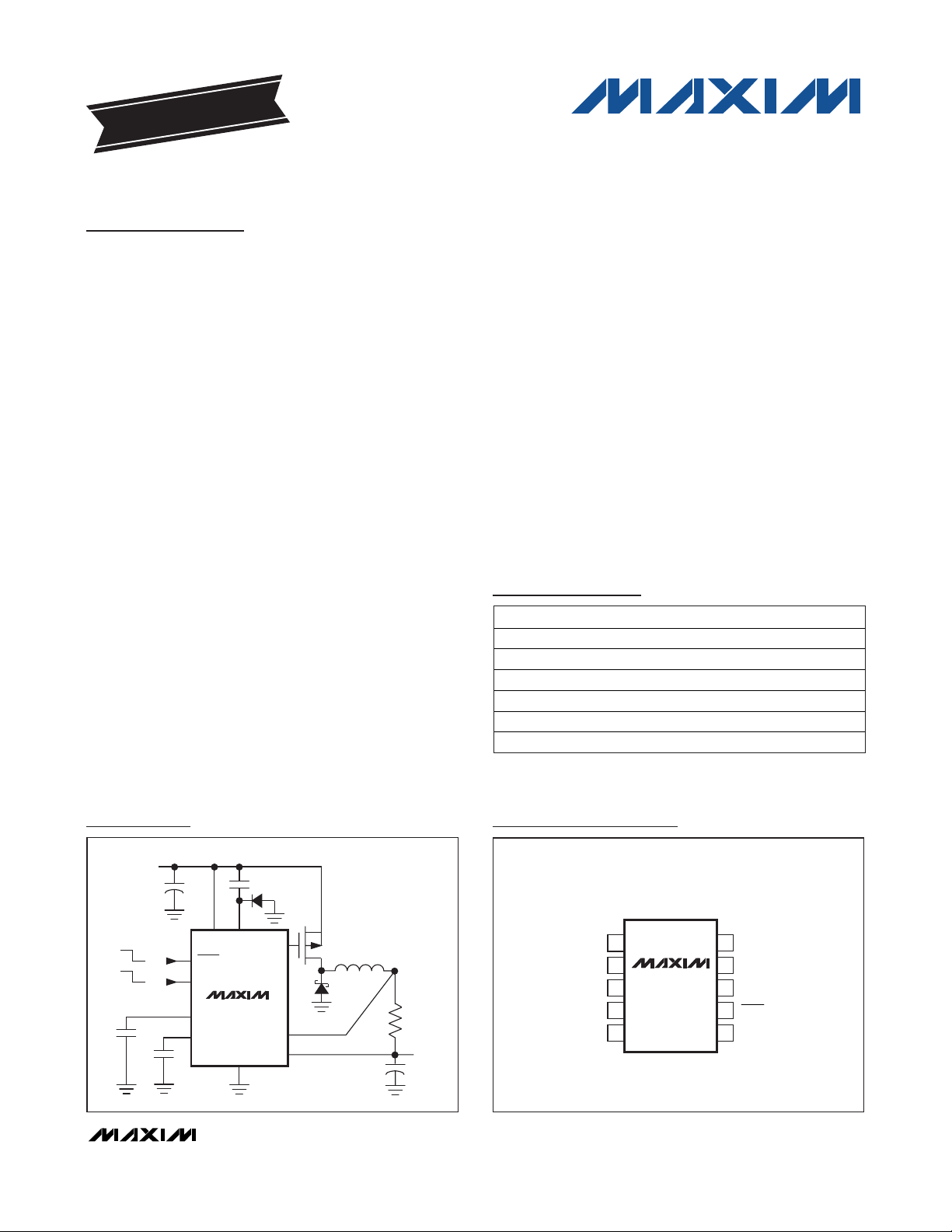
Typical Operating Circuit
1
+
2
3
4
5
10
9
8
7
6
IN
EXT
VH
3/5 (FB)
( ) ARE FOR MAX1745 ONLY.
REF
VL
GND
MAX1744
MAX1745
μMAX
TOP VIEW
CSOUT
SHDN
Pin Configuration
For pricing, delivery, and ordering information, please contact Maxim Direct at 1-888-629-4642,
or visit Maxim's website at www.maxim-ic.com.
EVALUATION KIT
AVAILABLE
μMAX is a registered trademark of Maxim Integrated Products, Inc.
Firewire is a registered trademark of Apple, Inc.
IEEE is a registered service mark of the Institute of Electrical
and Electronics Engineers, Inc.
+
Denotes a lead(Pb)-free/RoHS-compliant package.
/V Denotes an automotive qualified part.
IN
4.5V TO 36V
ON
OFF
5V
3.3V
IN VH
SHDN
3/5
MAX1744
VL
REF
GND
EXT
CS
OUT
P
OUT
3.3V
OR 5V
Page 2
MAX1744/MAX1745
High-Voltage, Step-Down DC-DC
Controllers in µMAX
2 _______________________________________________________________________________________
ABSOLUTE MAXIMUM RATINGS
ELECTRICAL CHARACTERISTICS
(VIN= V
SHDN
= 5.5V to 36V, 3/5 = GND, I
LOAD
= 0, TA= 0°C to +85°C, unless otherwise noted. Typical values at VIN= V
SHDN
=
36V, TA= +25°C.)
Stresses beyond those listed under “Absolute Maximum Ratings” may cause permanent damage to the device. These are stress ratings only, and functional
operation of the device at these or any other conditions beyond those indicated in the operational sections of the specifications is not implied. Exposure to
absolute maximum rating conditions for extended periods may affect device reliability.
IN, EXT, SHDN to GND...........................................-0.3V to +38V
VH to GND..............................................................-0.3V to +34V
VH, EXT to IN............................................................-7V to +0.3V
CS, OUT to GND ....................................................-0.3V to +20V
FB, 3/5, REF to GND .....................................-0.3V to (VL + 0.3V)
VL to GND...................................................................-0.3V to 6V
Continuous Power Dissipation (T
A
= +70°C)
10-Pin μMAX (derate 5.6mW/°C above 70°C) .............444mW
Operating Temperature Range
MAX174_EUB ..................................................-40°C to +85°C
MAX174_AUB ................................................-40°C to +125°C
Junction Temperature......................................................+150°C
Storage Temperature Range .............................-65°C to +150°C
Lead Temperature (soldering, 10s) ................................+300°C
Input Voltage Range 4.5 36 V
Supply Current into IN V
Shutdown Supply Current SHDN = GND 4 12 μA
Output Voltage (MAX1744)
OUT Input Current (MAX1744) 3/5 = VL, V
FB Threshold Voltage (MAX1745) Falling edge, hysteresis = 8mV 1.22 1.25 1.28 V
FB Input Current (MAX1745) -50 50 nA
VH Output Voltage with Respect to IN VIN = 5.5V to 36V, IVH = 100μA to 20mA -6.0 -5.3 -4.3 V
VL Output Voltage VIN = 5.5V to 36V, IVL = 100μA to 2mA 4.5 5.0 5.5 V
VL Undervoltage Lockout 2.0 3.0 4.1 V
CS Threshold Voltage
CS Input Current
SHDN, 3/5 Logic-High Threshold VIN = 4.5V to 36V 2.4 V
SHDN, 3/5 Logic-Low Threshold VIN = 4.5V to 36V 0.4 V
3/5 Input Current SHDN = GND ±1μA
SHDN Input Current
EXT Resistance 820Ω
Minimum EXT Off-Time 1.5 2.0 2.5 μs
Minimum EXT On-Time 0.7 1.0 1.5 μs
Output Line Regulation Figure 1, 5.5V < VIN < 36V, I
Output Load Regulation Figure 1, VIN = 12V, 30mA < I
Reference Voltage I
REF Load Regulation 0 ≤ I
REF Line Regulation VIN = 4.5V to 36V, I
PARAMETER CONDITIONS MIN TYP MAX UNITS
= VIN = 5.5V to 36V 90 140 μA
SHDN
3/5 = VL 4.85 5.00 5.15
3/5 = GND 3.20 3.30 3.40
OUT
VCS = V
V
VCS = V
V
3/5 = GND ±1
V
OUT
= V
CS
OUT
OUT
= V
CS
OUT
= 36V 12
SHDN
= 0 1.22 1.25 1.28 V
REF
≤ 100μA 4 10 mV
REF
= 5V 28 44 μA
= 2.5V to 18V 85 100 115
= V
GND
= 2.5V to 18V 0 15 25
= V
GND
= 1A 5 mV/V
LOAD
< 2A 15 mV/A
LOAD
= 0 30 60 μV/V
REF
80 110 150
-25 0
mV
μA
μA
V
Page 3
MAX1744/MAX1745
High-Voltage, Step-Down DC-DC
Controllers in µMAX
_______________________________________________________________________________________ 3
ELECTRICAL CHARACTERISTICS
(VIN= V
SHDN
= 5.5V to 36V, 3/5 = GND, I
LOAD
= 0, TA= -40°C to +85°C, unless otherwise noted.) (Note 1)
Input Voltage Range 4.5 36 V
Supply Current into IN V
Shutdown Supply Current SHDN = GND 12 μA
Output Voltage (MAX1744)
OUT Input Current (MAX1744) 3/5 = VL, V
FB Threshold Voltage (MAX1745) Falling edge, hysteresis = 8mV 1.22 1.28 V
FB Input Current (MAX1745) -50 50 nA
VH Output Voltage with Respect to IN VIN = 5.5V to 36V, IVH = 100μA to 20mA -6.0V -4.3V V
VL Output Voltage VIN = 5.5V to 36V, IVL = 100μA to 2mA 4.5 5.5 V
VL Undervoltage Lockout 2.0 4.1 V
CS Threshold Voltage
CS Input Current
SHDN, 3/5 Logic-High Threshold VIN = 4.5V to 36V 2.4 V
SHDN, 3/5 Logic-Low Threshold VIN = 4.5V to 36V 0.4 V
3/5 Input Current SHDN = GND ±1μA
SHDN Input Current
EXT Resistance 20 Ω
Minimum EXT Off-Time 1.5 2.5 μs
Minimum EXT On-Time 0.7 1.5 μs
Reference Voltage I
REF Load Regulation 0 ≤ I
REF Line Regulation VIN = 4.5V to 36V, I
PARAMETER CONDITIONS MIN MAX UNITS
= VIN = 5.5V to 36V 140 μA
SHDN
3/5 = VL 4.85 5.15
3/5 = GND 3.20 3.40
= 5V 44 μA
OUT
VCS = V
V
= V
CS
VCS = V
V
= V
CS
3/5 = GND ±1
V
SHDN
= 0 1.22 1.28 V
REF
REF
= 2.5V to 18V 85 115
OUT
= V
OUT
GND
= 2.5V to 18V 0 25
OUT
= V
OUT
GND
= 36V 12
≤ 100μA 10 mV
= 0 60 μV/V
REF
80 150
-25 0
V
mV
μA
μA
Page 4
MAX1744/MAX1745
High-Voltage, Step-Down DC-DC
Controllers in µMAX
4 _______________________________________________________________________________________
ELECTRICAL CHARACTERISTICS
(VIN= V
SHDN
= 5.5V to 36V, 3/5 = GND, I
LOAD
= 0, TA= -40°C to +125°C, unless otherwise noted.) (Note 1)
Note 1: Specifications to -40°C are guaranteed by design, not production tested.
Input Voltage Range 4.5 36 V
Supply Current into IN V
Shutdown Supply Current SHDN = GND 15 μA
Output Voltage (MAX1744)
OUT Input Current (MAX1744) 3/5 = VL, V
FB Threshold Voltage (MAX1745) Falling edge, hysteresis = 8mV 1.22 1.28 V
FB Input Current (MAX1745) -50 50 nA
VH Output Voltage with Respect to IN VIN = 5.5V to 36V, IVH = 100μA to 20mA -6.0V -4.3V V
VL Output Voltage VIN = 5.5V to 36V, IVL = 100μA to 2mA 4.5 5.5 V
VL Undervoltage Lockout 1.6 4.1 V
CS Threshold Voltage
CS Input Current
SHDN, 3/5 Logic-High Threshold VIN = 4.5V to 36V 2.4 V
SHDN, 3/5 Logic-Low Threshold VIN = 4.5V to 36V 0.4 V
3/5 Input Current SHDN = GND ±1μA
SHDN Input Current
EXT Resistance 20 Ω
Minimum EXT Off-Time 1.5 2.5 μs
Minimum EXT On-Time 0.7 1.5 μs
Reference Voltage I
REF Load Regulation 0 ≤ I
REF Line Regulation VIN = 4.5V to 36V, I
PARAMETER CONDITIONS MIN MAX UNITS
= VIN = 5.5V to 36V 140 μA
SHDN
3/5 = VL 4.85 5.15
3/5 = GND 3.20 3.40
= 5V 44 μA
OUT
VCS = V
V
= V
CS
VCS = V
V
= V
CS
3/5 = GND ±1
V
SHDN
REF
= 2.5V to 18V 85 115
OUT
= V
OUT
GND
= 2.5V to 18V 0 25
OUT
= V
OUT
GND
= 36V 12
= 0 1.22 1.28 V
≤ 100μA 10 mV
REF
= 0 80 μV/V
REF
80 150
-25 0
V
mV
μA
μA
Page 5
MAX1744/MAX1745
High-Voltage, Step-Down DC-DC
Controllers in µMAX
_______________________________________________________________________________________
5
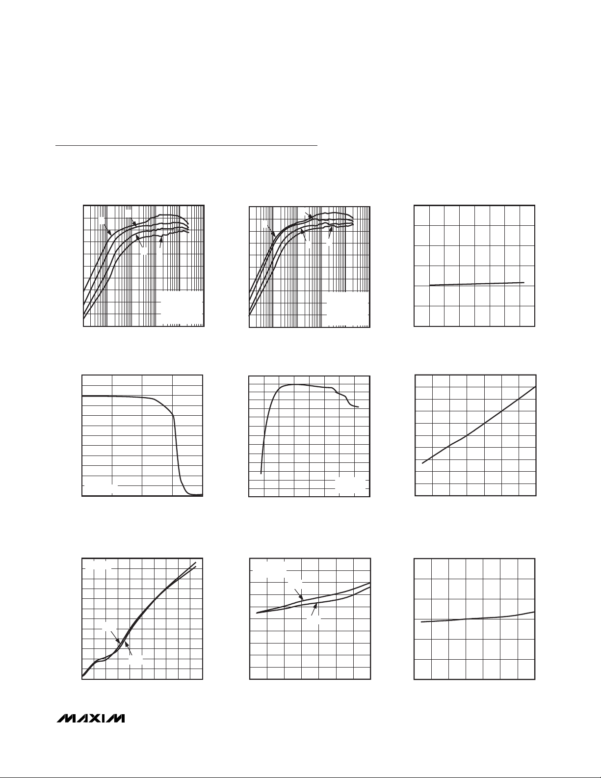
EFFICIENCY
(%)
Typical Operating Characteristics
(Circuit of Figure 1, TA = +25°C, unless otherwise specified.)
EFFICIENCY vs. LOAD CURRENT
= +3.3V)
(V
A
OUT
B
C
D
LOAD CURRENT (A)
A: VIN = +5.5V
B: V
C: V
D: V
100
80
60
40
EFFICIENCY (%)
20
0
0.0001 0.001 0.01 0.1 1 10
= +12.0V
IN
= +24.0V
IN
= +36.0V
IN
100
MAX1744/5toc01
EFFICIENCY vs. LOAD CURRENT
A
80
60
40
20
0
0.0001 0.001 0.01 0.1 1 10
IN PIN QUIESCENT CURRENT
vs. INPUT VOLTAGE (3.5V TO 5.5V)
6
5
4
3
2
QUIESCENT CURRENT (mA)
1
V
= 3.3V
OUT
0
3.5 4.5 5.5
INPUT VOLTAGE (V)
140
120
MAX1744/5toc04
100
80
60
40
SWITCHING FREQUENCY (kHz)
20
0
0 10203040
= +5.0V)
(V
OUT
B
D
C
A: VIN = +7.2V
B: V
IN
C: V
IN
D: V
IN
LOAD CURRENT (A)
SWITCHING FREQUENCY
vs. INPUT VOLTAGE
V
OUT
I
OUT
INPUT VOLTAGE (V)
= +12.0V
= +24.0V
= +36.0V
= 3.3V
= 2.0A
MAX1744/5toc02
MAX1744/5toc05
IN PIN QUIESCENT CURRENT
vs. INPUT VOLTAGE (5.5V TO 36V)
110
105
100
95
90
QUIESCENT CURRENT (μA)
85
80
0 10203040
INPUT VOLTAGE (V)
IN PIN QUIESCENT CURRENT
vs. TEMPERATURE
95
94
93
92
91
90
89
88
QUIESCENT CURRENT (μA)
87
86
85
-50 125
TEMPERATURE (°C)
1007525 500-25
MAX1744/5toc03
MAX1744/5toc06
120
100
(ns)
FALL
AND t
RISE
t
80
60
40
20
0
0 1000
EXT RISE AND FALL TIMES
vs. CAPACITANCE
VIN = +5V
t
FALL
t
RISE
2000
CAPACITANCE (pF)
3000
4000 5000
MAX1744/5toc07
EXT RISE AND FALL TIMES
vs. TEMPERATURE
50
VIN = +5V
45
= 1000pF
C
L
40
35
(ns)
30
FALL
25
AND t
20
RISE
t
15
10
5
0
-50 125
t
RISE
t
FALL
TEMPERATURE (°C)
CURRENT-SENSE TRIP LEVEL
vs. TEMPERATURE
115
110
MAX1744/5toc08
105
100
95
CURRENT-SENSE TRIP LEVEL (mV)
90
1007525 500-25
85
-50 125
TEMPERATURE (°C)
MAX1744/5toc09
1007550250-25
Page 6

MAX1744/MAX1745
High-Voltage, Step-Down DC-DC
Controllers in µMAX
6 _______________________________________________________________________________________
Typical Operating Characteristics (continued)
(Circuit of Figure 1, TA = +25°C, unless otherwise specified.)
REFERENCE OUTPUT VOLTAGE CHANGE
vs. TEMPERATURE
5
4
3
2
1
0
-1
-2
-3
-4
REFERENCE OUTPUT VOLTAGE CHANGE (%)
-5
-50 125
TEMPERATURE (°C)
LOAD-TRANSIENT RESPONSE
A
ENTERING/EXITING SHUTDOWN
RL = 3.3Ω
MAX1744/5toc10
V
OUT
2V/div
SHUTDOWN
PULSE
5V/div
1007525 500-25
2ms/div
MAX1744/5toc11
LINE-TRANSIENT RESPONSE
MAX1744
MAX1744/5toc12
A
B
MAX1744/5toc13
B
50μs/div
VIN = 7.2V, V
A: V
OUT
B: LOAD CURRENT, 1A/div
= 3.3V, LOAD CURRENT = 0.1A TO 2A
OUT
, 50mV/div, 3.3V AC-COUPLED
V
= 5V, LOAD CURRENT = 1A
OUT
, 100mV/div, AC-COUPLED
A: V
OUT
, 6V TO 12V, 5V/div
B: V
IN
4ms/div
Page 7

MAX1744/MAX1745
High-Voltage, Step-Down DC-DC
Controllers in µMAX
_______________________________________________________________________________________ 7
Detailed Description
The MAX1744/MAX1745 are high-voltage step-down
DC-DC converter controllers. These devices offer high
efficiency over a wide range of input/output voltages
and currents, making them optimal for use in applications such as telecom, automotive, and industrial control. Using an external P-channel MOSFET and
current-sense resistor allows design flexibility and
improved efficiency. The MAX1744/MAX1745 automatically switch from PWM operation at medium and heavy
loads to pulse-skipping operation at light loads to
improve light-load efficiency. The low 90μA quiescent
current further optimizes these parts for applications
where low input current is critical. Operation to 100%
duty cycle allows the lowest possible dropout voltage,
which allows a wider input voltage variation. The small
size, high switching frequency, and low parts count
minimize the required circuit board area and component cost. Figure 1 shows the MAX1744 typical application circuit.
Operating Modes
When delivering low output currents, the MAX1744/
MAX1745 operate in discontinuous-conduction mode.
Current through the inductor starts at zero, rises as
high as the current limit, then ramps down to zero during each cycle (Figure 3). The switch waveform exhibits
ringing, which occurs at the resonant frequency of the
inductor and stray capacitance, due to residual energy
trapped in the core when the commutation diode (D1 in
Figure 1) turns off.
When delivering medium-to-high output currents, the
MAX1744/MAX1745 operate in PWM continuous-conduction mode (Figure 4). In this mode, current always
flows through the inductor and never ramps to zero.
The control circuit adjusts the switch duty cycle to
maintain regulation without exceeding the peak switching current set by the current-sense resistor.
Pin Description
PIN
MAX1744 MAX1745
1 GND GND Ground
2VL VL
3 REF REF
4 3/5 —
4— FB
5 OUT OUT
6CS CS
7 SHDN SHDN
8VH VH
9 EXT EXT Gate Drive for External P-Channel MOSFET. EXT swings between IN and VH.
NAME
FUNCTION
5V Linear Regulator Output. VL provides power to the internal circuitry and can supply up
to 1mA to an external load. Bypass VL to GND with 4.7μF or greater capacitor.
1.25V Reference Output. REF can supply up to 100μA to an external load. Bypass REF to
GND with a 0.1μF or greater ceramic capacitor.
3.3V or 5V Selection. Connect 3/5 to GND to set the output voltage to 3.3V. Connect 3/5 to
VL to set the output voltage to 5V.
Feedback Input for Adjustable Output Operation. Connect to an external voltage-divider
between the output and FB to set the output voltage. The regulation voltage threshold is
1.25V.
Sense Input for Fixed 5V or 3.3V Output Operation (MAX1744) and Negative Current-Sense
Input (MAX1744/5). OUT is connected to an internal voltage-divider (MAX1744). OUT does
not supply current.
Current-Sense Input. Connect the current-sense resistor between CS and OUT. External
MOSFET is turned off when the voltage across the resistor is equal to or greater than the
current limit trip level (100mV).
Active-Low Shutdown Input. Connect SHDN to IN for normal operation. Drive SHDN to low
to shut the part off. In shutdown mode, the reference, output, external MOSFET, and
internal regulators are turned off.
High-Side Linear Regulator Output. VH provides a regulated output voltage that is 5V below
IN. The external P-channel MOSFET gate is driven between IN and VH. Bypass VH to IN
with a 4.7μF or greater capacitor (see the Capacitor Selection section).
10 IN IN Positive Supply Input. Bypass IN to GND with a 0.47μF or greater ceramic capacitor.
Page 8

MAX1744/MAX1745
High-Voltage, Step-Down DC-DC
Controllers in µMAX
8 _______________________________________________________________________________________
100% Duty Cycle and Dropout
The MAX1744/MAX1745 operate with a duty cycle up to
100%. This feature extends the input voltage range by
turning the MOSFET on continuously when the supply
voltage approaches the output voltage. This services
the load when conventional switching regulators with
less than 100% duty cycle would fail. Dropout voltage is
defined as the difference between the input and output
voltages when the input is low enough for the output to
drop out of regulation. Dropout depends on the
MOSFET drain-to-source on-resistance, current-sense
resistor, and inductor series resistance, and is proportional to the load current:
Regulation Control Scheme
The MAX1744/MAX1755 have a unique operating
scheme that allows PWM operation at medium and high
current, with automatic switching to pulse-skipping
mode at lower currents to improve light-load efficiency.
Figure 2 shows the simplified block diagram.
Under medium- and heavy-load operation, the inductor
current is continuous and the part operates in PWM
mode. In this mode, the switching frequency is set by
either the 1μs minimum on-time or the 2μs minimum offtime, depending on the duty cycle. The duty cycle is
approximately the output voltage divided by the input
voltage. If the duty cycle is less than 33%, the minimum
on-time controls the frequency; and the frequency is
approximately f ≈ 1MHz ✕D, where D is the duty cycle.
If the duty cycle is greater than 33%, the off-time sets the
frequency; and the frequency is approximately f ≈ 500kHz
✕
(1 - D).
In both cases, the voltage is regulated by the error
comparator. For low duty cycles (<33%), the MOSFET
is turned on for the minimum on-time, causing fixed-ontime operation. During the MOSFET on-time, the output
voltage rises. Once the MOSFET is turned off, the voltage drops to the regulation threshold (set by the internal voltage-divider for the MAX1745 and by the external
voltage-divider for the MAX1744), at which time another
cycle is initiated. For high duty cycles (>33%), the
MOSFET remains off for the minimum off-time, causing
fixed-off-time operation. In this case, the MOSFET
remains on until the output voltage rises to the regulation threshold. Then the MOSFET turns off for the minimum off-time, initiating another cycle.
By switching between fixed-on-time and fixed-off-time
operation, the MAX1744/MAX1745 can operate at high
input-output ratios, yet still operate up to 100% duty
cycle for low dropout. Note that when transitioning from
fixed-on-time to fixed-off-time operation, the output voltage drops slightly due to the output ripple voltage. In
fixed-on-time operation, the minimum output voltage is
regulated, but in fixed-off-time operation, the maximum
output voltage is regulated. Thus, as the input voltage
drops below approximately three times the output voltage, a decrease in line regulation can be expected.
The drop in voltage is approximately V
DROP
≈ V
RIPPLE
/ 2.
At light output loads, the inductor current is discontinuous, causing the MAX1744/MAX1745 to operate at
Figure 1. Typical Application Circuit
INPUT
4.5V TO 36V
C2
OFF
3.3V
0.47μF
SHDN
3/5
MAX1744
VL
REF
4.7μF
LOW ESR
ON
5V
IN
GND
C3
4.7μF
D2
VH
EXT
CS
OUT
M1
P
FAIRCHILD
NDS9407
L1
22μH
D1
NIHON
EC2IQ506
R
SENSE
40mΩ
OUT
3.3V OR 5V
2A
C1
220μF
Dropout voltage=
IxR +R
OUT DS(ON) SENNSE INDUCTOR
⎡
⎣
+R
⎤
⎦
Page 9

MAX1744/MAX1745
High-Voltage, Step-Down DC-DC
Controllers in µMAX
_______________________________________________________________________________________ 9
lower frequencies, reducing the MOSFET gate drive
and switching losses. In discontinuous mode, under
most circumstances, the on-time will be the fixed minimum on-time of 1μs. If the inductor value is small, or
the current-sense resistor large, the current limit will be
tripped before the minimum on-time, terminating the
on-time and thus setting the fixed on-time.
If the inductance is too large, or the output capacitance
high and equivalent series resistance (ESR) low, then
the MOSFET remains on longer than the minimum ontime, until the output capacitor charges beyond the
error comparator’s (V
OUT
/ 1.25V) ✕8mV hysteresis,
causing the part to operate in hysteretic mode.
Operating in hysteretic mode results in lower frequency
operation. The transition to hysteretic mode occurs at
the critical output capacitor ESR:
ESR
CRITICAL
= (V
OUT
/ 1.25V) ✕8mV / I
RIPPLE
where I
RIPPLE
is the inductor ripple current, and can be
determined by:
I
RIPPLE
= (VIN- V
OUT
) ✕t
ON(MIN)
/ L
where t
ON(MIN)
is the minimum on-time (1μs) for mini-
mum on-time-control, or:
I
RIPPLE
= (V
OUT
) ✕t
OFF(MIN)
/ L
where t
OFF(MIN)
is the minimum off-time (2μs) for mini-
mum off-time-control.
Figure 2. Simplified Functional Diagram
SHDN
EXT
IN
VH
VH
LINEAR
REGULATOR
VL
VL
LINEAR
REGULATOR
Q TRIG
MINIMUM
ON-TIME
ONE SHOT
Q TRIG
MINIMUM
OFF-TIME
ONE SHOT
REFERENCE
ERROR
COMPARATOR
Q
RS
REF
1.25
OUT
(FB)
3/5
SHDN
( ) MAX1745 ONLY
- - - MAX1744 ONLY
+
-
100mV
CS
Page 10

MAX1744/MAX1745
High-Voltage, Step-Down DC-DC
Controllers in µMAX
10 ______________________________________________________________________________________
VL Linear Regulator
The MAX1744/MAX1745 contain a 5V low-side linear regulator (VL) that powers the internal circuit and can supply
up to 1mA to an external load. This allows the
MAX1744/MAX1745 to operate up to 36V input, while
maintaining low quiescent current and high switching frequency. When the input voltage goes below 5.5V, this
regulator goes into dropout and the IN pin quiescent current will rise. See the
Typical Operating Characteristics
.
Bypass VL with a 4.7μF or greater capacitor.
VH Linear Regulator
The MAX1744/MAX1745 contain a high-side linear regulator (VH) that regulates its output to 5V below IN (the
positive supply input voltage). This regulator limits the
external P-channel MOSFET gate swing (EXT), allowing
high input voltage operation without exceeding the
MOSFET gate-source breakdown. Bypass VH with a
4.7μF or greater capacitor between IN and VH. Fast line
transients may drive the voltage on VH negative. The
clamp diode (D2) prevents damage to the IC during
such a condition. A Schottky diode with a minimum 40V
reverse rating such as the Nihon EP05Q04 is sufficient
for most applications.
Quiescent Current
The devices’ typical quiescent current is 90μA.
However, actual applications draw additional current to
supply MOSFET switching currents, OUT pin current,
external feedback resistors (if used), and both the diode
and capacitor leakage currents. For example, in the circuit of Figure 1, with IN at 30V and V
OUT
at 5V, typical
no-load supply current for the entire circuit is 100μA.
Shutdown Mode
When SHDN is low, the device enters shutdown mode. In
this mode, the internal circuitry is turned off. EXT is pulled
to IN, turning off the external MOSFET. The shutdown
supply current drops to less than 10μA. SHDN is a logiclevel input. Connect SHDN to IN for normal operation.
Reference
The 1.25V reference is suitable for driving small external
loads. It has a guaranteed 10mV maximum load regulation while sourcing load currents up to 100μA. The reference is turned off during shutdown. Bypass the
reference with 0.1μF for normal operation. Place the
bypass capacitor within 0.2in (5mm) of REF, with a direct
trace to GND.
Design Information
Setting the Output Voltage
The MAX1744’s output voltage can be selected to 3.3V
or 5V under logic control by using the 3/5 pin. Connect
the 3/5 pin to GND to ensure a 3.3V output, or connect
the 3/5 pin to V
L
to ensure a 5V output.
The MAX1745’s output voltage is set using two resistors, R2 and R3 (Figure 5), which form a voltage-divider
between the output and FB. R2 is given by:
where V
REF
= 1.25V. Since the input bias current at FB
has a maximum value of 50nA, large values (10kΩ to
200kΩ) can be used for R3 with no significant accuracy
Figure 3. Discontinuous-Conduction Mode, Light-Load-Current
Waveform
Figure 4. Continuous-Conduction Mode, Heavy-Load-Current
Waveform
A
B
C
10μs/div
CIRCUIT OF FIGURE 1, VIN = 18V, V
A: MOSFET DRAIN, 10V/div
B: OUT, 50mV/div, 3.3V DC OFFSET
C: INDUCTOR CURRENT, 1A/div
OUT
= 3.3V, I
LOAD
= 100mA
A
B
C
10μs/div
CIRCUIT OF FIGURE 1, VIN = 18V, V
A: MOSFET DRAIN, 10V/div
B: OUT, 50mV/div, 3.3V DC OFFSET
C: INDUCTOR CURRENT, 1A/div
OUT
= 3.3V, I
LOAD
R2= R3 x
⎛
V
OUT
⎜
V
⎝
REF
⎞
−
1
⎟
⎠
= 1.5A
Page 11

MAX1744/MAX1745
High-Voltage, Step-Down DC-DC
Controllers in µMAX
______________________________________________________________________________________ 11
loss. For 1% error, the current through R2 should be at
least 100 times FB’s input bias current.
Current-Sense-Resistor Selection
The current-sense comparator limits the peak switching
current to V
CS/RSENSE
, where R
SENSE
is the value of
the current-sense resistor and V
CS
is the current-sense
threshold. V
CS
is typically 100mV. Minimizing the peak
switching current will increase efficiency and reduce
the size and cost of external components. However,
since available output current is a function of the peak
switching current, the peak current limit must not be set
too low.
Set the peak current limit to 1.3 times the maximum
load current by setting the current-sense resistor to:
Inductor Selection
The essential parameters for inductor selection are inductance and current rating. The MAX1744/MAX1745 operate with a wide range of inductance values. In many
applications, values between 4.7μH and 100μH take best
advantage of the controller’s high switching frequency.
Calculate the minimum inductance value as follows:
where 1μs is the minimum on-time. Inductor values
between 2 and 10 times L
(MIN)
are recommended. With
high inductor values, the MAX1744/MAX1745 begin
continuous-conduction operation at a lower fraction of
the full load (see the
Detailed Description
section).
The inductor’s saturation and heating current ratings
must be greater than the peak switching current to prevent overheating and core saturation. Saturation occurs
when the inductor’s magnetic flux density reaches the
maximum level the core can support, and inductance
starts to fall. The heating current rating is the maximum
DC current the inductor can sustain without overheating.
For optimum efficiency, the inductor windings’ resistance should be less than the current-sense resistance.
If necessary, use a toroid, pot-core, or shielded-core
inductor to minimize radiated noise. Table 1 lists inductor types and suppliers for various applications.
External Switching Transistor
The MAX1744/MAX1745 drive a P-channel enhancement-mode MOSFET. The EXT output swings from VH
to IN. Be sure that the MOSFET’s on-resistance is specified for 5V gate drive or less. Table 1 recommends
MOSFET suppliers.
Four important parameters for selecting a P-channel
MOSFET are drain-to-source breakdown voltage, current rating, total gate charge (Q
g
), and R
DS(ON)
. The
drain-to-source breakdown voltage rating should be at
least a few volts higher than V
IN
. Choose a MOSFET
with a maximum continuous drain-current rating higher
than the peak current limit:
The Qg specification should be 80nC or less to ensure
fast drain voltage rise and fall times, and reduce power
losses during transition through the linear region. Q
g
specifies all of the capacitances associated with charging
the MOSFET gate. EXT pin rise and fall times vary with different capacitive loads, as shown in the
Typical Operating
Characteristics
. R
DS(ON)
should be as low as practical to
reduce power losses while the MOSFET is on. It should
be equal to or less than the current-sense resistor.
Figure 5. Adjustable-Output Operation Using the MAX1745
V
R=
CS
1.3 x I
CS(MIN)
OUT(MAX)
V-V
()
L=
(MIN)
IN OUT
V
CS MIN
xs
1μ
()
R
CS
FROM
OUTPUT
R2
TO FB
R3
V
CS MAX
I
D(MAX LIM MA X
I
≥=
)()
()
R
SENSE
Page 12

MAX1744/MAX1745
High-Voltage, Step-Down DC-DC
Controllers in µMAX
12 ______________________________________________________________________________________
Diode Selection
The MAX1744/MAX1745’s high switching frequency
demands a high-speed rectifier. Schottky diodes, such
as the 1N5817–1N5822 family or surface-mount equivalents, are recommended. Ultra-high-speed rectifiers
with reverse recovery times around 50ns or faster
should be used for high output voltages, where the
increased forward drop causes less efficiency degradation. Make sure that the diode’s peak current rating
exceeds the peak current limit set by R
SENSE
, and that
its breakdown voltage exceeds V
IN
. Schottky diodes
are preferred for heavy loads due to their low forward
voltage, especially in low-voltage applications. For
high-temperature applications, some Schottky diodes
may be inadequate due to their high leakage currents.
In such cases, ultra-high-speed rectifiers are recommended, although a Schottky diode with a higher
reverse voltage rating can often provide acceptable
performance.
Capacitor Selection
Choose filter capacitors to service input and output
peak currents with acceptable voltage ripple. ESR in
the output capacitor is a major contributor to output ripple, so low-ESR capacitors are recommended. LowESR tantalum, polymer, or ceramic capacitors are best.
Low-ESR aluminum electrolytic capacitors are tolerable, but standard aluminum electrolytic capacitors are
not recommended.
Voltage ripple is the sum of contributions from ESR and
the capacitor value:
For tantalum capacitors, the ripple is determined by the
ESR, but for ceramic capacitors, the ripple is mostly
due to the capacitance. Voltage ripple as a consequence of ESR is approximated by:
The ripple due to the capacitance is approximately:
Estimate input and output capacitor values for given
voltage ripple as follows:
where I
ΔL
is the change in inductor current.
These equations are suitable for initial capacitor selection; final values should be set by testing a prototype or
evaluation kit. When using tantalum capacitors, use
good soldering practices to prevent excessive heat
from damaging the devices and increasing their ESR.
Also, ensure that the tantalum capacitors’ surge-current
ratings exceed the startup inrush and peak switching
currents.
Pursuing output ripple lower than the error comparator’s hysteresis (0.6% of the output voltage) is not practical, since the MAX1744/MAX1745 will switch at slower
frequencies, increasing inductor ripple current threshold. Choose an output capacitor with a working voltage
rating higher than the output voltage.
The input filter capacitor reduces peak currents drawn
from the power source and reduces noise and voltage
Table 1. Component Suppliers
COMPANY COUNTRY PHONE FAX
803-946-0690
AVX USA
Coilcraft
Coiltronics
Dale/Vishay
Kemet
Inter nati onal
Recti fi er
IRC
Motorola
Nichicon
Nihon
Sanyo
Sprague
Sumida
United
Chemi-Con
USA
USA
USA
USA
USA 310-322-3331 310-322-3332
USA
USA
USA
Japan
USA
Japan
USA
Japan
USA
USA
Japan
USA 714-255-9500 714-255-9400
or
800-282-4975
847-639-6400 847-639-1469
516-241-7876 516-241-9339
402-564-3131 402-563-6418
408-986-0424 408-986-1442
512-992-7900 512-992-3377
602-303-5454 602-994-6430
847- 843- 7500
81- 7- 5231- 8461
805- 867- 2555
81- 3- 3494- 7411
619- 661- 6835
81- 7- 2070- 6306
408-988-8000
orSiliconix USA
800-554-5565
603-224-1961 603-224-1430
847- 956- 0666
81- 3- 3607- 5111
803-626-3123
847-843-2798
81-7-5256-4158
805-867-2698
81-3-3494-7414
619-661-1055
81-7-2070-1174
408-970-3950
847-956-0702
81-3-3607-5144
V
RI PPLE
V
C
=
IN
C
OUT
≈+
VV
RI PPLE,ESR
V
RI PPLE,C
1
2
LI
Δ
2
VV
RIPPLE CIN IN
,
=
V
RI PPL
EECOUT OUTININ OUT
,,
RI PPLE ESR RI PPLE C
≈−()R
≈
L
1
2
LI
Δ
2
,
Δ
ESRIpp
2
LI
PEAK
2CV
L
V
O
⎛
V
⎜
VV
−
⎝
⎞
⎟
⎠
Page 13

MAX1744/MAX1745
High-Voltage, Step-Down DC-DC
Controllers in µMAX
______________________________________________________________________________________ 13
ripple at IN, caused by the circuit’s switching action.
Use a low-ESR capacitor. Two smaller-value low-ESR
capacitors can be connected in parallel if necessary.
Choose input capacitors with working voltage ratings
higher than the maximum input voltage.
Place a surface-mount ceramic capacitor very close to
IN and GND. This capacitor bypasses the MAX1744/
MAX1745, minimizing the effects of spikes and ringing
on the power source (IN).
Bypass REF with 0.1μF. This capacitor should be
placed within 0.2 inches (5mm) of the IC, next to REF,
with a direct trace to GND.
Layout Considerations
High-frequency switching regulators are sensitive to PC
board layout. Poor layout introduces switching noise into
the current and voltage feedback signals and may
degrade performance. The current-sense resistor must
be placed within 0.2 inches (5mm) of the controller IC,
directly between OUT and CS. Place voltage feedback
resistors (MAX1745) next to the FB pin (no more than
0.2in) rather than near the output. Place the 0.47μF input
bypass capacitor within 0.2in (5mm) of IN.
Refer to the MAX1744 Evaluation Kit manual for a twolayer PC board example.
Chip Information
PROCESS: BiCMOS
Page 14

MAX1744/MAX1745
High-Voltage, Step-Down DC-DC
Controllers in µMAX
14 ______________________________________________________________________________________
Note: MAX1744/MAX1745 do not feature exposed pads.
PACKAGE TYPE PACKAGE CODE DOCUMENT NO.
10 μMAX U10CN+1
21-0061
Package Information
For the latest package outline information and land patterns, go to www.maxim-ic.com/packages.
10LUMAX.EPS
α
α
Page 15

High-Voltage, Step-Down DC-DC
Controllers in µMAX
MAX1744/MAX1745
Maxim cannot assume responsibility for use of any circuitry other than circuitry entirely embodied in a Maxim product. No circuit patent licenses are
implied. Maxim reserves the right to change the circuitry and specifications without notice at any time.
Maxim Integrated Products, 120 San Gabriel Drive, Sunnyvale, CA 94086 408-737-7600 ____________________
15
© 2009 Maxim Integrated Products Maxim is a registered trademark of Maxim Integrated Products, Inc.
Revision History
REVISION
NUMBER
0 7/00 Initial release. —
2 8/06 — —
3 4/09 Added lead-free and automot ive qua lified packages to Ordering Information. 1–4, 10, 13
4 8/09 Added MAX1744 automotive package to Ordering Information. 1
REVISION
DATE
DESCRIPTION
PAGES
CHANGED
 Loading...