

Page 1
For free samples and the latest literature, visit www.maxim-ic.com or phone 1-800-998-8800.
For small orders, phone 1-800-835-8769.
General Description
The MAX1740/MAX1741 subscriber identity module
(SIM)/smart card level translators provide level shifting
and electrostatic discharge (ESD) protection for SIM and
smart card ports. These devices integrate two unidirectional level shifters for the reset and clock signals, a bidirectional level shifter for the serial data stream, and
±10kV ESD protection on all card contacts.
The MAX1740 includes a SHDN control input to aid
insertion and removal of SIM and smart cards, while the
MAX1741 includes a system-side data driver to support
system controllers without open-drain outputs. The logic
supply voltage range is +1.425V to +5.5V for the “controller side” and +2.25V to +5.5V for the “card side.”
Total supply current is 2.5µA max. Both devices automatically shut down when either power supply is removed.
For a complete SIM-card interface, combine the
MAX1740/MAX1741 with the MAX1686H 0V/3V/5V regulated charge pump.
The MAX1740/MAX1741 are available in ultra-small 10pin µMAX packages that are only 1.09mm high and half
the area of an 8-pin SO.
The MAX1740/MAX1741 are compliant with GSM test
specifications 11.11 and 11.12.
Applications
SIM Interface in GSM Cellular Telephones
Smart Card Readers
Logic Level Translation
SPI™/QSPI™/MICROWIRE™ Level Translation
Features
♦ SIM/Smart Card Level Shifting
♦ ±10kV ESD Card Socket Protection
♦ Allows Level Translation with DV
CC
≥ V
CC
or
DV
CC
≤ V
CC
♦ Automatically Shuts Down When Either Supply Is
Removed
♦ Card Contacts Actively Pulled Low During
Shutdown
♦ +1.425V to +5.5V Controller Voltage Range
♦ +2.25V to +5.5V Card Voltage Range
♦ 2.5µA (max) Total Quiescent Supply Current
♦ 0.01µA Total Shutdown Supply Current
♦ Ultra-Small 10-Pin µMAX Package
♦ Compliant with GSM Test Specifications 11.11
and 11.12
MAX1740/MAX1741
SIM/Smart Card Level Translators
in µMAX
________________________________________________________________ Maxim Integrated Products 1
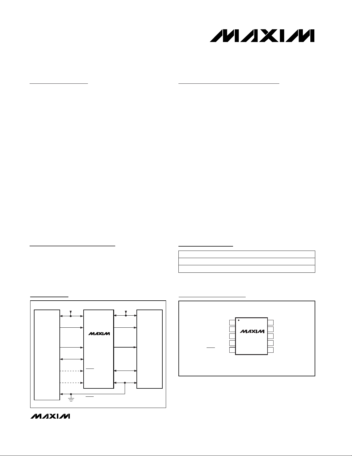
Typical Operating Circuit
19-1458; Rev 0; 1/00
PART
MAX1740EUB
MAX1741EUB
-40°C to +85°C
-40°C to +85°C
TEMP. RANGE PIN-PACKAGE
10 µMAX
10 µMAX
Pin Configuration
Ordering Information
SPI and QSPI are trademarks of Motorola, Inc.
MICROWIRE is a trademark of National Semiconductor Corp.
DV
SYSTEM
CONTROLLER
GND
CC
DV
CC
OPTIONAL
OPTIONAL
DV
CC
RIN
MAX1740
MAX1741
CIN
DATA
SHDN*
DDRV*
*
SHDN FOR MAX1740 ONLY
DDRV FOR MAX1741 ONLY
CLK
GND GND
V
CC
V
CC
IO
V
RSTRST
CLK
IO
CC
SIM OR
SMART
CARD
TOP VIEW
IO1DATA
10
DV
2
CC
CIN
3
MAX1740
RIN
( ) ARE FOR MAX1741.
MAX1741
4
5
µMAX
9
V
CC
CLK
8
RST
7
GNDSHDN (DDRV)
6
Page 2
MAX1740/MAX1741
SIM/Smart Card Level Translators
in µMAX
2 _______________________________________________________________________________________
ABSOLUTE MAXIMUM RATINGS
ELECTRICAL CHARACTERISTICS
(Figure 1, DVCC= +1.8V, VCC= +3.0V or +5.0V, SHDN = DVCC, CIN = RIN = GND or DVCC, IO = VCC, DATA = DDRV = DVCC,
C
IO
= C
CLK
= C
RST
= C
DATA
= 30pF, TA= 0°C to +85°C, unless otherwise noted. Typical values are at TA= +25°C.)
Stresses beyond those listed under “Absolute Maximum Ratings” may cause permanent damage to the device. These are stress ratings only, and functional
operation of the device at these or any other conditions beyond those indicated in the operational sections of the specifications is not implied. Exposure to
absolute maximum rating conditions for extended periods may affect device reliability.
DVCC, VCCto GND................................................-0.3V to +6.0V
RIN, CIN, DATA, DDRV,
SHDN to GND......................................-0.3V to (DV
CC
+ 0.3V)
RST, CLK, IO to GND ................................-0.3V to (V
CC
+ 0.3V)
Continuous Power Dissipation (T
A
= +70°C)
10-Pin µMAX (derate 5.6mW/°C above +70°C) ..........444mW
Operating Temperature Range ..........................-40°C to +85°C
Storage Temperature Range ............................-65°C to +150°C
Junction Temperature......................................................+150°C
Lead Temperature (soldering, 10s) ................................+300°C
UNITS
DVCCOperating Range DV
CC
1.425 5.5
V
V
CC
Operating Range V
CC
2.25 5.5
V
DVCCOperating Current I
DVCC
CIN static
1
µA
CIN clocked at 1.625MHz from GND to DV
CC
with 50% duty cycle
CONDITIONS
8
CIN clocked at 3.25MHz from GND to DV
CC
with 50% duty cycle
16
VCCOperating Current I
VCC
CIN static
1.5
mA
CIN clocked at 1.625MHz from GND to DV
CC
with 50% duty cycle
0.5
CIN clocked at 3.25MHz from GND to DV
CC
with 50% duty cycle
1
Total Shutdown Current I
SHDN
I
OFF
= I
VCC
+ I
DVCC
, SHDN = GND
(MAX1740 only), or DV
CC
= GND
or VCC= GND
0.01 2
µA
Digital Input Low Threshold V
IL
0.2 · DV
CC
V
Digital Input High Threshold V
IH
0.7 · DV
CC
V
Input Leakage Current
0.01 1
µA
Digital Output Low Level V
OL
I
SINK
= 200µA
0.4
V
Digital Output High Level V
OH
I
SOURCE
= 20µA
0.9 · V
CC
V
I
SOURCE
= 200µA
0.8 · V
CC
DATA Pull-Up Resistance R
DATA
Between DATA and DV
CC
13 20 28
kΩ
Input Low Threshold V
IL(DATA)
(Note 1)
0.3
V
Input High Threshold V
IH(DATA)
(Note 2)
DVCC- 0.6
V
Input Low Current I
IL
VCC= 5.0V
1
mA
MIN TYP MAXSYMBOLPARAMETER
Input High Current I
IH
2
µA
POWER SUPPLIES
CIN, RIN, SHDN, DDRV LOGIC INPUTS
CLK, RST OUTPUTS
DATA INPUT/OUTPUT
µA
Page 3
MAX1740/MAX1741
SIM/Smart Card Level Translators
in µMAX
_______________________________________________________________________________________ 3
ELECTRICAL CHARACTERISTICS (continued)
(Figure 1, DVCC= +1.8V, VCC= +3.0V or +5.0V, SHDN = DVCC, CIN = RIN = GND or DVCC, IO = VCC, DATA = DDRV = DVCC,
C
IO
= C
CLK
= C
RST
= C
DATA
= 30pF, TA= 0°C to +85°C, unless otherwise noted. Typical values are at TA= +25°C.)
UNITS
DVCC= 2.7V
DVCC= 2.25V
CONDITIONS
DVCC= 1.7V
DVCC= 1.425V
DVCC= 2.25V
DVCC= 1.7V
DVCC= 1.425V
MIN TYP MAXSYMBOLPARAMETER
Output Low Level V
OL(DATA)
IO = GND, I
SINK
= 100µA
0.4
V
DVCC= 3.0V, IO = GND, I
SINK
= 200µA
0.4
V
Output High Level
I
SOURCE
= 10µA
0.7 · DV
CC
V
DVCC= 3.0V, I
SOURCE
= 20µA
0.7 · DV
CC
V
V
OH(DATA)
IO Pull-Up Resistance R
IO
Between IO and V
CC
6.5 10 14
kΩ
Input Low Threshold V
IL(IO)IIL(MAX)
= 1mA (Note 1)
0.3
V
Input High Threshold V
IH(IO)IIH(MAX)
= ±20µA (Note 2)
0.7 · V
CC
V
Input Low Current I
IL
1
mA
Input High Current I
IH
20
µA
Output Low Level V
OL(IO)
DATA = GND or DDRV = GND,
I
SINK
= 200µA
0.4
V
Output High Level V
OH(IO)ISOURCE
= 20µA
0.8 · V
CC
V
Shutdown Output Levels
(IO, CLK, RST)
I
SINK
= 200µA, SHDN = GND, DATA = CIN =
RIN = DV
CC
(MAX1740 only)
0.4
V
I
SINK
= 200µA, DVCC= GND, SHDN
(MAX1740) = DDRV (MAX1741) = DATA =
CIN = RIN = DV
CC
0.4
V
I
SINK
= 200µA, VCC= GND, SHDN
(MAX1740) = DDRV (MAX1741) = DATA =
CIN = RIN = DV
CC
0.4
V
Maximum CLK Frequency
(Notes 3, 4)
f
CLK
VCC= 2.7V to 5.5V
5
MHz
5
5
3.5
VCC= 2.25V to 3.6V
4
4
3.5
IO INPUT/OUTPUT
SHUTDOWN OUTPUT LEVELS
TIMING
Page 4
MAX1740/MAX1741
SIM/Smart Card Level Translators
in µMAX
4 _______________________________________________________________________________________
ELECTRICAL CHARACTERISTICS
(Figure 1, DVCC= +1.8V, VCC= +3.0V or +5.0V, SHDN = DVCC, CIN = RIN = GND or DVCC, IO = VCC, DATA = DDRV = DVCC,
C
IO
= C
CLK
= C
RST
= C
DATA
= 30pF, TA= -40°C to +85°C, unless otherwise noted.) (Note 5)
UNITS
µAI
DVCC
DVCCOperating Current
µA
DVCCOperating Range DV
CC
1.425 5.5
V
VCCOperating Range V
CC
2.25 5.5
V
I
VCC
VCCOperating Current
CIN static
1
CIN static
1.5
CONDITIONS
Total Shutdown Current I
OFF
I
OFF
= I
VCC
+ I
DVCC
, SHDN = GND
(MAX1740 only), or DV
CC
= GND
or VCC= GND
2
µA
I
SOURCE
= 200µA
0.8 · V
CC
V
IO Pull-Up Resistance R
IO
Between IO and V
CC
6.5 14
Digital Input Low Threshold V
IL
0.2 · DV
CC
V
kΩ
Input Low Threshold V
IL(IO)
Input Leakage Current
1
µA
Digital Output Low Level V
OL
I
SINK
= 200µA
0.4
V
Digital Output High Level V
OH
I
SOURCE
= 20µA
0.9 · V
CC
MIN MAXSYMBOLPARAMETER
DATA Pull-Up Resistance R
DATA
Between DATA and DV
CC
13 28
kΩ
I
IL(MAX)
= 1mA (Note 1)
0.3
Input Low Threshold
V
(Note 1) 0.3 VV
IL(DATA)
Output Low Level
Input High Threshold V
IH(DATA)
(Note 2)
DV
CC
-
0.6
V
Output Low Level V
OL(DATA)
IO = GND, I
SINK
= 100µA
0.4
V
DVCC= 3.0V, IO = GND, I
SINK
= 200µA
0.4
V
Output High Level V
OH(DATA)
I
SOURCE
= 10µA
0.7 · DV
CC
V
DVCC= 3.0V, I
SOURCE
= 20µA
0.7 · DV
CC
V
V
OL(IO)
DATA = GND or DDRV = GND, I
SINK
= 200µA
0.4
V
Input High Threshold V
IH(IO)IIH(MAX)
= ±20µA (Note 2)
0.7 · V
CC
V
Output High Level V
OH(IO)ISOURCE
= 20µA
0.8 · V
CC
V
Digital Input High Threshold V
IH
0.75 · DV
CC
V
Input Low Current I
IL
VCC= 5.0V
1
mA
Input High Current I
IH
2
µA
Input Low Current I
IL
1
mA
Input High Current I
IH
20
µA
POWER SUPPLIES
CIN, RIN, SHDN, DDRV LOGIC INPUTS
CLK, RST OUTPUTS
DATA INPUT/OUTPUT
IO INPUT/OUTPUT
Page 5

MAX1740/MAX1741
SIM/Smart Card Level Translators
in µMAX
_______________________________________________________________________________________ 5
ELECTRICAL CHARACTERISTICS (continued)
(Figure 1, DVCC= +1.8V, VCC= +3.0V or +5.0V, SHDN = DVCC, CIN = RIN = GND or DVCC, IO = VCC, DATA = DDRV = DVCC,
C
IO
= C
CLK
= C
RST
= C
DATA
= 30pF, TA= -40°C to +85°C, unless otherwise noted.) (Note 5)
UNITSCONDITIONS
I
SINK
= 200µA, SHDN = GND, DATA =
CIN = RIN = DV
CC
(MAX1740 only)
0.4
MIN MAXSYMBOLPARAMETER
V
Note 1: VILis defined as the voltage at which the output (DATA/IO) voltage equals 0.5V.
Note 2: V
IH
is defined as the voltage at which the output (DATA/IO) voltage exceeds the input (IO/DATA) voltage by 100mV.
Note 3: Timing specifications are guaranteed by design, not production tested.
Note 4: The maximum CLK frequency is defined as the output duty cycle remaining in the 40% to 60% range when the 50% CIN is
applied. CIN has 5ns rise and fall times; levels are GND to DV
CC
. Input and output levels are measured at 50% of the waveform.
Note 5: Specifications to -40°C are guaranteed by design, not production tested.
Typical Operating Characteristics
(Circuit of Figure 1, DVCC= 3.0V, VCC= 5.0V, DDRV or DATA = DVCC, RIN = CIN = GND, TA= +25°C, unless otherwise noted.)
0.5
0.7
0.9
1.1
1.3
1.7
1.5
-40 -15 10 35 60 85
TOTAL OPERATING SUPPLY
CURRENT vs. TEMPERATURE
MAX1740toc03
TEMPERATURE (°C)
SUPPLY CURRENT, I
VCC
+ I
DVCC
(mA)
V
DVCC
= 3.0V, fIN = 3.25MHz, CIN CLOCKED
WITH A 0 TO 3V SQUARE WAVE
DATA OR DDRV = DV
CC
V
VCC
= 3.0V
DATA OR DDRV = DV
CC
V
VCC
= 5.0V
f
DATA
= f
CIN
/372
V
VCC
= 5.0V
f
DATA
= f
CIN
/372
V
VCC
= 3.0V
0
0.2
0.4
0.6
0.8
1.0
1.2
1.4
1.6
1.8
2.0 2.5 3.0 3.5 4.0 4.5 5.0 5.5
TOTAL OPERATING SUPPLY CURRENT
vs. SUPPLY VOLTAGE (VCC)
MAX1740/1toc01
VCC (V)
SUPPLY CURRENT, I
VCC
+ I
DVCC
(mA)
DATA OR DDRV = DV
CC
f
CIN
= 3.25MHz
DATA OR DDRV = DV
CC
f
CIN
= 1.625MHz
f
DATA
= f
CIN
/372
f
CIN
= 1.625MHz
f
DATA
= f
CIN
/372
f
CIN
= 3.25MHz
V
DVCC
= 3.0V
CIN CLOCKED WITH A
0 TO 3V SQUARE WAVE
0
0.5
1.0
1.5
2.0
2.5
0 0.5 1.0 1.5 2.0 2.5 3.0 3.5 4.0 4.5 5.0
TOTAL OPERATING SUPPLY
CURRENT vs. CLOCK FREQUENCY
MAX1740toc02
f
CIN
(MHz)
SUPPLY CURRENT, I
VCC
+ I
DVCC
(mA)
V
DVCC
= 3.0V
CIN CLOCKED WITH A
0 TO 3V SQUARE WAVE
DATA OR DDRV = DV
CC
V
VCC
= 5.0V
DATA OR DDRV = DV
CC
V
VCC
= 5.0V
f
DATA
OR f
CIN
/372
V
VCC
= 5.0V
f
DATA
OR f
CIN
/372
V
VCC
= 5.0V
DVCC= 2.7V
VCC= 2.7V to 5.5V
DVCC= 1.7V
DV
CC
= 1.425V
DV
CC
= 2.25V
DVCC= 1.7V
DVCC= 2.25V
5
DVCC= 1.425V
3.5
Maximum CLK Frequency
(Notes 3, 4)
f
CLK
5
MHz
5
3.5
VCC= 2.25V to 3.6V
4
4
I
SINK
= 200µA, DVCC= GND, SHDN
(MAX1740) = DDRV (MAX1741) = DATA =
CIN = RIN = DV
CC
0.4
V
I
SINK
= 200µA, VCC= GND, SHDN
(MAX1740) = DDRV (MAX1741) = DATA =
CIN = RIN = DV
CC
0.4
V
SHUTDOWN OUTPUT LEVELS
TIMING
Shutdown Output Levels
(IO, CLK, RST)
Page 6

MAX1740/MAX1741
SIM/Smart Card Level Translators
in µMAX
6 _______________________________________________________________________________________
Typical Operating Characteristics (continued)
(Circuit of Figure 1, DVCC= 3.0V, VCC= 5.0V, DDRV or DATA = DVCC, RIN = CIN = GND, TA= +25°C, unless otherwise noted.)
40ns/div
CIN TO CLK WAVEFORM
3V
0
0
5V
CIN
1V/div
CLK
2V/div
MAX1740/1toc04
f
CIN
= 3.25MHz
40ns/div
RIN TO RST WAVEFORM
0
0
3V
5V
RIN
1V/div
RST
2V/div
MAX1740/1toc05
f
RIN
= 3.25MHz
1ms/div
UNDERVOLTAGE
SHUTDOWN WAVEFORM
0
1V
1.5V
V
CC
0.5V/div
CLK, RST, OR IO
0.5V/div
0
MAX1740/1toc08
1µs/div
DDRV TO IO AND DATA WAVEFORM
(MAX1741 ONLY)
3V
5V
0
0
3V
0
DDRV
2V/div
DATA
2V/div
IO
2V/div
MAX1740/1toc09
Page 7

MAX1740/MAX1741
SIM/Smart Card Level Translators
in µMAX
_______________________________________________________________________________________ 7
NAME
2 2 DV
CC
3 3 CIN
4 4 RIN
— 5 DDRV
8 8 CLK
7 7 RST
6 6 GND
5 —
SHDN
10 10 IO
9 9 V
CC
Pin Description
Card-Side Bidirectional Input/Output. An open-drain output with a 10kΩ pull-up resistor to
VCC. For bidirectional data transfer, connect to an open-drain card output capable of sinking 1mA while pulling IO low. Actively pulled low during shutdown.
Supply Voltage for Card-Side Digital Pins. Set at +2.25V to +5.5V. Proper supply bypassing is required to meet ±10kV ESD specifications.
Clock Output to Card. Actively pulled low during shutdown.
Reset Output to Card. Actively pulled low during shutdown.
System Controller and Card Ground
Shutdown Mode Input. Driving SHDN low reduces the total supply current to less than
2µA. In shutdown mode, RST, CLK, and IO are actively pulled low and the transfer gate
between DATA and IO is disabled. When not used, connect SHDN to DV
CC
.
Optional System Controller Data Input. Connect to controllers without an open-drain output. When not used, connect DDRV to DVCC.
System Controller Reset Input
System Controller Clock Input
Supply Voltage for System Controller Digital Pins. Set at +1.425V to +5.5V.
FUNCTION
1 DATA1
System Controller Data Input/Output. An open-drain input/output with a 20kΩ pull-up
resistor to DVCC. For bidirectional data transfer, connect to an open-drain controller output
capable of sinking 1mA while pulling DATA low. If the controller is not open drain, use
DDRV to send data and DATA to receive data.
MAX1740 MAX1741
PIN
Detailed Description
The MAX1740/MAX1741 provide the necessary level
translation for interfacing with subscriber identity modules (SIMs) and smart cards in multivoltage systems.
These devices operate with logic supply voltages
between +1.425V and +5.5V on the controller side
(DVCC) and between +2.25V and +5.5V on the card side
(VCC). The total supply current (I
DV
CC
+ I
V
CC
) is 2.5µA
(max) while operating in an idle state (see Electrical
Characteristics). Figure 2 shows a typical application circuit and functional diagram.
Level Translation
The MAX1740/MAX1741 provide level translators for a
clock input, a reset input, and a bidirectional data
input/output. The clock and reset inputs (CIN and RIN)
are level shifted from the controller-side supply rails
(DVCCto GND) to the card-side supply rails (VCCto
GND). When connected to an open-drain controller output, DATA and IO provide bidirectional level translation.
Figure 1. MAX1740/MAX1741 Test Circuit
MAX1740
+1.8V
30pF
*
SHDN FOR MAX1740 ONLY
DDRV FOR MAX1741 ONLY
NOTE: ALL CAPACITANCES INCLUDE CAPACITIVE LOADS OF
TEST PROBES AND BOARD LAYOUT.
DV
CC
SHDN*
RIN
CIN
DDRV*
DATA
MAX1741
V
RST
CLK
GND
CC
IO
30pF
+3.0V OR
+5.0V
30pF 30pF
Page 8

MAX1740/MAX1741
All level translation is valid for DVCC≥ VCCor DVCC≤
VCC. The MAX1740/MAX1741 contain internal pull-up
resistors from DATA to the controller-side supply
(DVCC) and from IO to the card-side supply (VCC). For
push-pull controller outputs, see the Data Driver section
for bidirectional data translation.
Data Driver (MAX1741 only)
When using a microcontroller (µC) without an open-drain
output, use the data driver (DDRV) input to send data to
the SIM/smart card, while DATA provides the controllerside output for bidirectional data transfer. When not
used, connect DDRV to DVCCto reduce total supply current.
Shutdown Mode
For the MAX1740, drive SHDN low to activate shutdown. Connect SHDN to DVCCor drive high for normal
operation. To allow for card insertion and removal, shutdown mode actively pulls CLK, RST, and IO low; it also
disconnects the internal 10kΩ pull-up resistor from V
CC
to prevent excessive current draw. Shutdown mode
reduces the total supply current (I
DVCC
+ I
VCC
) to
0.01µA.
SIM/Smart Card Insertion/Removal
The SIM/smart card specifications require that the
card-side pins (V
CC
, CLK, RST, IO) be at ground
potential prior to inserting the SIM/smart card. For
applications using the MAX1686H (Figure 4), the easi-
est way to achieve this is by shutting down the
MAX1686H or by driving SHDN (MAX1740 only) low. If
specific sequencing is desired, pull IO low by driving
either DATA or DDRV (MAX1741 only) low, and pull
CLK and RST low by driving CIN and RIN low, respectively.
ESD Protection
As with all Maxim devices, ESD-protection structures
on all pins protect against electrostatic discharges
(ESDs) encountered during handling and assembly.
For further protection during card insertion and
removal, the pins that connect to the card socket (CLK,
RST, IO, V
CC
, and GND) provide protection against
±10kV of ESD, according to the Human Body Model.
The ESD structures withstand high ESD in all states:
normal operation, shutdown, and power-down. After an
ESD event, the MAX1740/MAX1741 continue working
without latchup.
ESD Test Conditions
ESD performance depends on a variety of conditions.
Contact Maxim for a reliability report documenting test
setup, test methodology, and test results.
Human Body Model
Figure 3a shows the Human Body Model, and Figure
3b shows the current waveform it generates when discharged into a low impedance. This model consists of
a 100pF capacitor charged to the ESD voltage of inter-
SIM/Smart Card Level Translators
in µMAX
8 _______________________________________________________________________________________
Figure 2. Typical Application Circuit and Functional Diagram
DV
CC
DV
1µF
CC
RIN
CIN
DATA
SHDN*
DDRV*
20k 10k
SHUTDOWN
CONTROL
MAX1740
MAX1741
DV
CC
SYSTEM
CONTROLLER
OPTIONAL
OPTIONAL
GND
*
SHDN FOR MAX1740 ONLY
DDRV FOR MAX1741 ONLY
V
RST
CLK
GND
CC
V
CC
V
CC
RST
1µF
CLK
SIM OR
SMART CARD
IO
IO
GND
Page 9

MAX1740/MAX1741
SIM/Smart Card Level Translators
in µMAX
_______________________________________________________________________________________ 9
est, which is then discharged into the test device
through a 1.5kΩ resistor.
Applications Information
SIM/Smart Card Interface
To provide 5V when interfacing with a 5V SIM/smart
card, 3V systems require a DC-DC converter. The
MAX1686H +5V regulating charge pump for SIM cards
provides 0V/3V/5V for full compatibility with SIM/smart
card specifications. Figure 4 shows the charge pump
for SIM card applications. Alternatively, the MAX619
generates a regulated 5V from input voltages as low as
2V.
SPI/QSPI/MICROWIRE Interface
The MAX1740/MAX1741 are also useful as 3V/5V level
shifters in SPI, QSPI, and MICROWIRE applications
(Figure 5). On the slave side, connect CLK to SCLK,
RST to CS, and IO to DOUT and DIN. The unidirectional
level shifters transfer chip select and clock signals to
the slave device(s), while the bidirectional level shifter
transfers data.
HIGH-
Figure 3a. Human Body ESD Test Model
Figure 3b. Human Body Model Current Waveform
Figure 4. Using MAX1740/MAX1741 and MAX1686/MAX1686H
Charge Pump for SIM Card Applications
Figure 5. MAX1740/MAX1741 with SPI/QSPI/MICROWIRE
Interfaces
TRANSISTOR COUNT: 114
___________________Chip Information
VOLTAGE
DC
SOURCE
R
C
1M
CHARGE-CURRENT
LIMIT RESISTOR
C
100pF
R
D
1500Ω
DISCHARGE
RESISTANCE
STORAGE
s
CAPACITOR
DEVICE
UNDER
TEST
AMPERES
IP 100%
90%
36.8%
10%
0
0
t
RL
TIME
t
DL
CURRENT WAVEFORM
PEAK-TO-PEAK RINGING
I
r
(NOT DRAWN TO SCALE)
+3.0V
DV
SYSTEM
CONTROLLER
GND
CC
OPTIONAL
OPTIONAL
*
SHDN FOR MAX1740 ONLY
DDRV FOR MAX1741 ONLY
CXN CXP
IN
MAX1686
MAX1686H
3/5
SHDN
MAX1740
MAX1741
DV
CC
RIN
CIN
DATA
SHDN*
DDRV*
3.0V OR 5.0V
OUT
GND
PGND
V
CC
RST
CLK
IO
GND GND
IO
V
RST
CLK
SIM OR
CC
SMART
CARD
+5.0V
DV
SYSTEM
CONTROLLER
GND
CC
OPTIONAL
OPTIONAL
*
SHDN FOR MAX1740 ONLY
DDRV FOR MAX1741 ONLY
IN
MAX8867
MAX8860
SHDN
DV
CC
RIN
CIN
DATA
SHDN*
DDRV*
MAX1740
MAX1741
OUT
SET
PGND
V
CC
RST
CLK
IO
GND GND
+3.3V
SPI/QSPI/
MICROWIRE
SYSTEM
V
CC
CS
SCLK
DOUT
DIN
Page 10

MAX1740/MAX1741
SIM/Smart Card Level Translators
in µMAX
10 ______________________________________________________________________________________
________________________________________________________Package Information
Note: The MAX1740/MAX1741 do not have an exposed pad.
10LUMAX.EPS
Page 11

MAX1740/MAX1741
SIM/Smart Card Level Translators
in µMAX
______________________________________________________________________________________ 11
NOTES
Page 12

MAX1740/MAX1741
SIM/Smart Card Level Translators
in µMAX
Maxim cannot assume responsibility for use of any circuitry other than circuitry entirely embodied in a Maxim product. No circuit patent licenses are
implied. Maxim reserves the right to change the circuitry and specifications without notice at any time.
12 ____________________Maxim Integrated Products, 120 San Gabriel Drive, Sunnyvale, CA 94086 408-737-7600
© 2000 Maxim Integrated Products Printed USA is a registered trademark of Maxim Integrated Products.
NOTES
 Loading...