

Page 1
EVALUATION KIT
FOLLOWS DATA SHEET
ECB and LCD Display Bias Supply with Accurate
Output Voltage and Temperature Compensation
General Description
The MAX1729 micropower step-up/step-down DC-DC
converter is ideally suited for electrically controlled birefringence (ECB) and liquid-crystal-display (LCD) biassupply generation. It provides step-up/step-down
voltage conversion and reduces output ripple by using
a step-up DC-DC converter followed by a linear regulator. This architecture permits a physically smaller inductor than those used in competing SEPIC and flyback
topologies. This device features low quiescent current
(67µA typical). A logic-controlled shutdown mode further reduces quiescent current to 0.4µA typical.
The MAX1729 features an input that dynamically
adjusts the output voltage to control display color or
contrast. It offers two feedback modes: internal and
external. Internal feedback mode allows output voltages between 2.5V and 16V, and is specifically
designed to hold temperature drift to ±11ppm/°C.
External feedback mode allows the MAX1729 output
voltage range to be tailored for various displays.
An on-chip temperature sensor with a positive temperature coefficient provides compensation for LCD/ECB
display temperature characteristics. In internal feedback mode, the buffered temperature sensor output is
read and used to adjust the output voltage via a digital
control signal. External feedback mode features an
additional compensation method in which the temperature output is summed directly into the feedback network to provide first-order negative temperature
compensation of the output voltage. The MAX1729 is
available in the space-saving 10-pin µMAX package.
Applications
ECB Display Bias & Color Adjustment
LCD Display Bias & Contrast Adjustment
Cellular Phones
Personal Digital Assistants
Features
♦ High-Accuracy Reference Voltage (±1%)
♦ ±11ppm/°C Output Voltage Drift
♦ On-Chip Temperature Sensor Output
♦ Accurate Voltage and Temperature Provide:
Consistent ECB Colors
Consistent LCD Gray-Scale Contrast
♦ +2.7V to +5.5V Input Voltage Range
♦ Output Voltage Range
+2.5V to +16V in Internal Feedback Mode
Programmable in External Feedback Mode
♦ Dynamic Control of the Output Voltage
♦ 67µA Supply Current
♦ 0.4µA Shutdown Current
♦ 10-Pin µMAX Package (1.09mm max height)
♦ Evaluation Kit Available (MAX1729EVKIT)
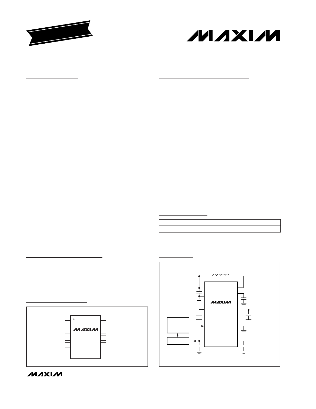
MAX1729
________________________________________________________________
Maxim Integrated Products
1
PS
OUT
FB
COMP
LX
TC
CTLIN
V
OUT
+2.5V to +16V
DIGITAL
PWM
CONTROLLER
GND
IN
V
IN
2.7V to 5.5V
MAX1729
REF
ADC
Typical Operating Circuit
19-1406; Rev 1; 1/99
PART
MAX1729EUB -40°C to +85°C
TEMP. RANGE PIN-PACKAGE
10 µMAX
Ordering Information
Pin Configuration
1
2
3
4
5
10
9
8
7
6
GND
LX
PS
OUTCOMP
REF
TC
IN
MAX1729
µMAX
TOP VIEW
CTLINFB
For free samples & the latest literature: http://www.maxim-ic.com, or phone 1-800-998-8800.
For small orders, phone 1-800-835-8769.
Page 2
MAX1729
ECB and LCD Display Bias Supply with Accurate
Output Voltage and Temperature Compensation
2 _______________________________________________________________________________________
ABSOLUTE MAXIMUM RATINGS
ELECTRICAL CHARACTERISTICS
(VIN= +3V, CTLIN = IN, FB = GND, TA= -40°C to +85°C, unless otherwise noted. Typical values are at TA= +25°C.) (Note 1)
Stresses beyond those listed under “Absolute Maximum Ratings” may cause permanent damage to the device. These are stress ratings only, and functional
operation of the device at these or any other conditions beyond those indicated in the operational sections of the specifications is not implied. Exposure to
absolute maximum rating conditions for extended periods may affect device reliability.
IN to GND.................................................................-0.3V to +6V
LX, PS, OUT to GND...............................................-0.3V to +20V
CTLIN, FB, REF, COMP, TC to GND ...........-0.3V to (V
IN
+ 0.3V)
LX to PS..................................................................-20V to +1.0V
LX, PS, OUT Current...........................................................60mA
Continuous Power Dissipation (T
A
= +70°C)
10-pin µMAX (derate 5.6mW/°C above +70°C)..........444mW
Operating Temperature Range ...........................-40°C to +85°C
Junction Temperature......................................................+150°C
Storage Temperature Range.............................-65°C to +160°C
Lead Temperature (soldering, 10sec).............................+300°C
CONDITIONS
V2.7 5.5V
IN
Operating Voltage Range
UNITSMIN TYP MAXSYMBOLPARAMETER
V2.0 2.6V
LO
Undervoltage Lockout
Threshold (Note 2)
µA37 50I
IN
IN Supply Current
µA30 40I
PS
PS Supply Current
µA0.4 2I
SHDN
Shutdown Supply Current CTLIN = GND, I
SHDN
= IIN+ I
PS
I
REF
= 0 V
1.215 1.228 1.241
V
REF
Reference Output Voltage
TA= +25°C
1.200 1.256TA= -40°C to +85°C
FB = GND, CTLIN =
0.1% duty cycle,
I
OUT
= 0 to 0.5mA
V
V
OUT
(MIN)
Minimum Output Voltage
2.35 2.45 2.5
TA= -40°C to +85°C
I
OUT
= 0 to 0.5mA V16 16.40
V
OUT
(MAX)
Maximum Output Voltage
FB = GND, CTLIN =
0.1% to 100% duty
cycle, I
OUT
= 0
V/100%CTLIN to V
OUT
Gain
13.90 13.95 14.00TA= 0°C to +85°C
VPS= +18V (Note 3) ppm/°C
±11 ±30
TC
OUT
Output Voltage
Temperature Coefficient
TA= 0°C to +85°C
±18 ±65TA= -40°C to +85°C
mA0.5 2.5I
OUT
Maximum Output Current
V1.178 1.228 1.278V
TC
TC Output Voltage TA= +25°C
mV/°C
15.5 16.5 17.5
TC
TC
TC Output Temperature
Coefficient (Note 3)
TA= 0°C to +85°C
14.5 16.5 18.5TA= -40°C to +85°C
µA±50I
TC
TC Output Current
TA= 0°C to +85°C
2.35 2.52
TA= -40°C to +85°C 13.60 14.20
V
1.215 1.228 1.241
V
FB
Feedback Set Voltage (FB)
TA= +25°C
1.200 1.256TA= -40°C to +85°C
mV90 122 150V
MODE
FB Mode Threshold
nA550I
FB
FB Bias Current VFB= +1.25V
V
2
V
IH
CTLIN High Voltage
VIN= +5.5V
1.3VIN= +2.7V
Page 3
MAX1729
ECB and LCD Display Bias Supply with Accurate
Output Voltage and Temperature Compensation
_______________________________________________________________________________________ 3
Note 1: Specifications to -40°C are guaranteed by design, not production tested.
Note 2: When V
IN
is below this level, the boost and LDO outputs are disabled.
Note 3: Guaranteed by design.
Note 4: Minimum time to hold CTLIN low to invoke shutdown. If CTLIN is held low for less than t
OFF
, device does not enter shutdown.
Note 5: Switching regulator regulates this voltage to keep LDO from dropping out.
ELECTRICAL CHARACTERISTICS
(VIN= +3V, CTLIN = IN, FB = GND, TA= -40°C to +85°C, unless otherwise noted. Typical values are at TA= +25°C.) (Note 1)
VFB= 0, Internal Feedback Mode
V0.4 0.6 1.0
VIN= +5.5V, CTLIN = GND or IN
VIN= +2.7V to +5.5V
PS to OUT Voltage (Note 5)
TA= +25°C
I
DIODE
= 30mA
(Note 4)
ILX= 30mA
ns25
CONDITIONS
511
V-µs
6810
KPFM On-Time Constant
t
CTLIN
CTLIN Minimum Pulse Width
for V
OUT
Control
VFB= +1.25V ns
Ω
60 150
R
COMP
COMP Impedance
µA±1I
IHL
V0.4V
IL
CTLIN Low Voltage
CTLIN Bias Current
20tR/t
F
COMP Rise/Fall Time
VIN= +5.5V 1.5
mV700 970V
LX-PS
LX to PS Diode Forward
Voltage
µs700 1250 2400t
OFF
CTLIN Minimum Pulse Width
for Shutdown
Ω
2.5 5.0
R
ON
Switch On-Resistance
UNITSMIN TYP MAXSYMBOLPARAMETER
VIN= +2.7V
VLX= 18V µA0.1 1I
LX(OFF)
Switch Off-Leakage Current
V
FB =
+1.25V, External Feedback Mode
33
kΩ
TA= -40°C to +85°C
Page 4
MAX1729
ECB and LCD Display Bias Supply with Accurate
Output Voltage and Temperature Compensation
4 _______________________________________________________________________________________
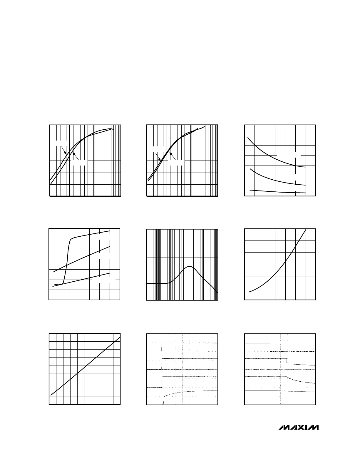
Typical Operating Characteristics
(Circuit of Figure 2, TA = +25°C, unless otherwise noted.)
0
0.01 1010.1
EFFICIENCY vs. OUTPUT CURRENT
V
OUT
= 9.4 (CTLIN AT 50% DUTY CYCLE)
20
10
30
60
50
40
MAX1729 toc 01
OUTPUT CURRENT (mA)
EFFICIENCY (%)
VIN = 5.5V
VIN = 2.7V
0
0.01 1010.1
EFFICIENCY vs. OUTPUT CURRENT
V
OUT
= 16.4 (CTLIN = IN)
20
10
30
60
50
40
MAX1729 toc 02
OUTPUT CURRENT (mA)
EFFICIENCY (%)
VIN = 5.5V
VIN = 2.7V
0.05
0.15
0.10
0.25
0.20
0.35
0.30
0.40
2.5 3.5 4.03.0 4.5 5.0 5.5 6.0
NO-LOAD SUPPLY CURRENT vs.
SUPPLY VOLTAGE
MAX1729 toc 03
SUPPLY VOLTAGE (V)
SUPPLY CURRENT (mA)
V
OUT
= 16.4V
V
OUT
= 9.4V
V
OUT
= 2.5V
0
2
1
4
3
6
5
7
2.5 3.5 4.03.0 4.5 5.0 5.5 6.0
MAXIMUM OUTPUT CURRENT vs.
SUPPLY VOLTAGE
MAX1729 toc 04
SUPPLY VOLTAGE (V)
MAXIMUM OUTPUT CURRENT (mA)
V
OUT
= +2.5V
V
OUT
= 9.4V
V
OUT
= 16.4V
0
4
2
8
6
10
12
16
14
18
0 20304010 50 60 70 80 90 100
OUTPUT VOLTAGE vs.
DUTY CYCLE
MAX1729 toc 07
DUTY CYCLE (%)
OUTPUT VOLTAGE (V)
0
-100
1 10 100 1k 10k 100k
PS TO OUT (LDO)
POWER-SUPPLY REJECTION RATIO
-80
MAX1729 toc 05
FREQUENCY (Hz)
PSRR (dB)
-60
-40
-20
0
1.0
0.5
2.0
1.5
2.5
3.0
2.5 4.0 4.53.0 3.5 5.0 5.5 6.0
SHUTDOWN SUPPLY CURRENT
MAX1729 toc 06
INPUT VOLTAGE (V)
SHUTDOWN CURRENT (µA)
20ms/div
START-UP DELAY FROM SHUTDOWN
V
CTLIN
5V/div
V
REF
1V/div
V
TC
1V/div
V
OUT
10V/div
MAX1729 toc 08
V
IN
= 5V
I
O
= 0.5mA
500ms/div
DELAY TO SHUTDOWN
V
CTLIN
5V/div
V
REF
1V/div
V
TC
1V/div
V
OUT
10V/div
MAX1729 toc 09a
V
IN
= 5V
I
O
= 0.5mA
Page 5

MAX1729
ECB and LCD Display Bias Supply with Accurate
Output Voltage and Temperature Compensation
_______________________________________________________________________________________ 5
5ms/div
DELAY TO SHUTDOWN
V
CTLIN
5V/div
V
REF
1V/div
V
TC
1V/div
V
OUT
10V/div
MAX1729 toc 09b
V
IN
= 5V
I
O
= 0.5mA
2µs/div
SWITCHING WAVEFORMS
HEAVY LOAD
I
L
20mA/div
OUTPUT
RIPPLE
10mV/div
V
LX
5V/div
MAX1729 toc 10
2µs/div
SWITCHING WAVEFORMS
MEDIUM LOAD
I
L
20mA/div
OUTPUT
RIPPLE
10mV/div
V
LX
5V/div
MAX1729 toc 11
Typical Operating Characteristics (continued)
(Circuit of Figure 2, TA= +25°C, unless otherwise noted.)
1ms/div
LOAD-TRANSIENT RESPONSE
V
OUT
20mV/div
I
OUT
250µA/div
20µA
500µA
16.400
16.404
MAX1729 toc 13
2ms/div
LINE-TRANSIENT RESPONSE
V
OUT
20mV/div
V
IN
1V/div
4V
5V
MAX1729 toc 14
CTLIN = IN
I
OUT
= 0.5mA
Page 6

MAX1729
Detailed Description
The MAX1729 is designed to provide bias voltage for
ECB or LCD displays. It is composed of a step-up
DC-DC converter followed by a linear regulator
(Figure 1), a combination that provides step-up/stepdown voltage conversion while minimizing output ripple. The device allows you to adjust a display’s color or
contrast by dynamically adjusting the MAX1729’s output voltage using a PWM control signal. In internal
feedback mode, the output voltage is adjustable
between +2.5V and +16V. In external feedback mode,
the output voltage is adjustable, and its range is set by
a resistor network that is programmed to match the output voltage range of LCD/ECB displays needing a maximum output up to +18V.
Boost Converter
The MAX1729’s DC-DC boost converter is implemented
with an on-chip N-channel MOSFET, a diode, and an
error comparator. The IC’s unique PFM control system
varies the on-time and off-time of the switch based on the
boost converter’s input and output voltage values, as follows:
where K is typically 8V-µs. This timing maintains discontinuous conduction and sets the peak inductor current
(I
PEAK
) to:
where L is the inductance of L1 (Figures 2, 3, and 4).
When the error comparator detects that the drop across
the linear regulator (VPS- V
OUT
) is less than approximately 0.6V, the internal switch is turned on (tONinitiates) and
current through the inductor ramps to I
PEAK
. At the end of
tON, the switch is turned off for at least t
OFF
, allowing the
I =
K
L
PEAK
t =
K
V
t
K
VV
ON
IN
OFF
PS IN
≥−
ECB and LCD Display Bias Supply with Accurate
Output Voltage and Temperature Compensation
6 _______________________________________________________________________________________
Pin Description
Drain of the internal MOSFET SwitchLX9
GroundGND10
Feedback and Mode Control Input. Connect to GND for internal feedback mode operation.FB5
Control Input. Drive low for more than 1.2ms to put the device into shutdown.CTLIN6
Bypass to GND with a 1.0µF capacitor.OUT7
Output of boost converter and input to LDO. Bypass to GND with a 0.068µF capacitor.PS8
Compensation Pin. In internal feedback mode (Figure 2), bypass with a 1µF capacitor. In external feedback
mode, COMP is a buffered inverse version of CTLIN (Figure 3).
COMP4
Reference Voltage Output. Bypass to GND with a 0.1µF capacitor.REF3
PIN
Temperature-Sensor Output. Bypass to GND with a 1000pF capacitor.TC2
Supply Input. Bypass with 0.1µF capacitor to ground. Connect to supply side of inductor (L1).IN1
FUNCTIONNAME
Page 7

inductor current to ramp down and VPSto increase. If, at
the end of t
OFF
, VPS- V
OUT
is still too low, then another
tONis initiated immediately. Otherwise, the boost converter remains idle in a low-quiescent-current state until
VPS- V
OUT
drops again and the error comparator initi-
ates another cycle.
Linear Regulator
The PNP low-dropout linear regulator of the MAX1729
regulates the boost-converter output to the desired output voltage. The boost converter’s regulation circuitry
holds the linear regulator’s input voltage (VPS) approximately 0.6V above the output voltage to keep the regulator out of dropout, thereby enhancing ripple rejection.
The linear regulator incorporates short-circuit protection, which limits the output current to approximately
6mA.
Temperature Sensor Output
The MAX1729 generates a temperature sensor voltage
(VTC) that varies at 16.5mV/°C (typ) and is nominally
equal to the reference voltage at room temperature. TC
is capable of sinking or sourcing 50µA. This output is
used to compensate for ECB color or LCD contrast
variations caused by changes in temperature. It may
be read with an ADC and used to modify an external
PWM control signal or, in external feedback mode,
summed directly into the feedback-resistor network.
Control Signal
An externally generated PWM control signal on CTLIN
controls V
OUT
in internal feedback mode and influ-
ences V
OUT
in external feedback mode. In either mode,
if CTLIN is held low for longer than 1.24ms, the
MAX1729 enters shutdown mode, decreasing the supply current below 2µA. Shutdown mode limits the minimum duty cycle and frequency that may be used to
keep the device active. CTLIN frequencies between
2kHz and 12kHz are recommended.
Internal Feedback Mode
In internal feedback mode, the signal at CTLIN is inversely buffered, level-shifted, and output at COMP through a
resistor. Internal resistance (33kΩ typical) and C6 then filter the signal before it is used by the internal feedback
network to set V
OUT
. If temperature compensation is
used, the temperature sensor output voltage is read by
an ADC and used to adjust the duty cycle of the PWM
control signal. See the
Designing for Internal Feedback
Mode
section for more information.
External Feedback Mode
In external feedback mode, the output voltage of the
MAX1729 is controlled by the duty cycle of the PWM
control signal and an external resistor network, as
shown in Figure 3. In this mode, the signal at CTLIN is
inverted, level-shifted, and presented directly to COMP.
R3, R4, and C6 filter the signal, before it is summed into
the feedback node.
Design Procedure
Designing for Internal Feedback Mode
For a 3kHz PWM control signal use a 1µF low-leakage
ceramic capacitor for C6. For applications requiring a
higher-frequency PWM control signal, reduce the value
of C6 to between 1µF and 0.22µF for frequencies
between 3kHz and 12kHz. Higher C6 values reduce
output ripple. In Figure 2, V
OUT
is governed by the fol-
lowing equation:
where V
OUT(MIN)
is 2.45V and Gain is nominally
13.95V/100%, as listed in the
Electrical Characteristics.
V = V Duty Cycle Gain
OUT OUT(MIN)
+⋅
MAX1729
ECB and LCD Display Bias Supply with Accurate
Output Voltage and Temperature Compensation
_______________________________________________________________________________________ 7
122mV
V
REF
GND
NOTE: SWITCH STATES SHOWN FOR INTERNAL FEEDBACK MODE.
COMP
TC
LX
PS
OUT
MAX1729
IN
REF
FB
CTLIN
BOOST
CONVERTER
TEMPERATURE
SENSOR
VOLTAGE
REFERENCE
SHUTDOWN
CONTROL
LDO
LINEAR
REGULATOR
FEEDBACK
CONTROL
GND
Figure 1. Internal Block Diagram
Page 8

MAX1729
To use a DC control signal to adjust the output voltage,
use the circuit shown in Figure 4. In this configuration,
V
OUT
is governed by the following equation:
The impedance looking into COMP is nominally 33kΩ.
A source output impedance of less than 500Ω is recommended. Also, ensure V
OUT
≤ 18V by keeping
V
COMP
above 0.6V.
Designing for External Feedback Mode
To solve for V
OUT
in external feedback mode, assume
the current into the FB pin is zero and the voltage at FB
is 1.228V. Then take the sum of the currents into FB
and solve for V
OUT
:
Using the following formulas, calculate the external
component values required for MAX1729 operation in
external feedback mode, as shown in Figure 3. An
example follows the formulas.
External Component Value Formulas
1) Given the maximum output voltage needed (V
MAX
),
choose the maximum feedback current and solve for
R1 (10µA to 30µA is recommended for maximum feedback current) as follows:
R1 =
V - V
I
MAX FB
FB
V = R1
1R11
R21RR1R5
V
R1
RR
V
R1
R5
V
OUT FB
COMP TC
++
+
+
−
+
−
34
34
V 24.67V - 22.71V
OUT FB COMP
≈
ECB and LCD Display Bias Supply with Accurate
Output Voltage and Temperature Compensation
8 _______________________________________________________________________________________
PS
OUT
FB
COMP
LX
L1
220µH
TC
CTLIN
DIGITAL
PWM
CONTROLLER
GND
IN
V
IN
C1
0.1µF
C2
0.068µF
C4
1µF
C6
1µF
C3
0.1µF
C5
1000pF
V
OUT
MAX1729
REF
ADC
Figure 2. Internal Feedback Mode
PS
OUT
FB
TC
LX
L1
220µH
COMP
CTLIN
PWM
GENERATOR
GND
IN
V
IN
R4 R3
C1
0.1µF
C2
0.068µF
C4
1µF
R1
R5 R2
C6
1µF
C3
0.1µF
V
OUT
MAX1729
C5
1000pF
REF
Figure 3. External Feedback Mode
PS
OUT
FB
COMP
LX
L1
TC
CTLIN
GND
IN
220µH
V
IN
C1
0.1µF
C2
0.068µF
C4
1µF
V
COMP
DC CONTROL
INPUT
C3
0.1µF
C5
1000pF
V
OUT
MAX1729
REF
Figure 4. Using a DC Control Signal
Page 9

2) Given the maximum output voltage (V
MAX
) and mini-
mum output voltage (V
MIN
), calculate values for R3 and
R4 as follows:
3) For first-order temperature compensation, calculate
R5 as shown below. (If temperature compensation is
not used, leave R5 open.)
where Tempco is the negative temperature coefficient
needed to compensate the ECB or LCD display for
changes in temperature.
4) Solve for V
COMP
. The duty cycle used here corresponds to the duty cycle that yields the maximum output voltage, not including first-order temperature
compensation.
where a 90% duty cycle corresponds to Duty Cycle = 0.9.
5) Use the results from the above calculations to solve
for R2. (For applications not utilizing temperature compensation, use 1 / R5 = 0.)
External Component Value Example
The example application requires the output voltage to
adjust between 5V and 10V, using the circuit shown in
Figure 3. The device in our example needs a temperature coefficient of 33mV/°C, which yields the following
results.
1) V
MAX
= 10V and IFB= 29.24µA is within the limits
and yields a reasonable resistor value, therefore:
2) V
MAX
= 10V and V
MIN
= 5V, therefore:
with R3 = 36.7kΩ, then V
MIN
= 5.019V. Let R4 =
R3 = 36.7kΩ.
3) Tempco = 33mV/°C, therefore:
4) If external circuitry limits the duty cycle to 90%, the
following equation is true:
5) Solving for R2:
With R2 = 56kΩ, a duty cycle of 87.4% generates a
V
OUT
of 10V.
Component Selection
Inductors
Use a 220µH inductor to maximize output current
(2.5mA typical). Use an inductor with DC resistance
less than 10Ω and a saturation current exceeding
35mA. For lower peak inductor current, use a 470µH
inductor with DC resistance less than 20Ω and a saturation current over 18mA. This limits output current to
typically less than 1mA. See Table 1 for a list of recommended inductors. The inductor should be connected
from the battery to the LX pin, as close to the IC as possible.
Capacitors
The equivalent series resistance (ESR) of output capacitor C2 directly affects output ripple. To minimize output
ripple, use a low-ESR capacitor. A physically smaller
capacitor, such as a common ceramic capacitor, minimizes board space and cost while creating an output
ripple that’s acceptable in most applications. Refer to
Table 2 for recommended capacitor values.
1
R2
V
R1
V
R3
V
R5
1
V
1R11R31
R5
1
56560
OUT COMP FB
FB
=++
−++
=
V 1.228 1
0.9
2
0.6754V
COMP
=−
=
R5
300k
33mV/ C=°
°=ΩΩ / 16. mV k5 150C
R3 1/2
300k
5V
1.228 36,840=
=
Ω
Ω
R1
10V 1.228V
29.24 A
=
−
µ
= 300kΩ
1
R2
1
V
V
R1
V
R3VR5
1R11R31
R5
FB
OUT COMP FB
=++
−++
V =V 1 – Duty Cycle
R4
R3 R4
COMP FB
⋅
+
R5 =
R1
Tempco
16.5mV/ C
°
R3 = 1/2
R1
V – V
V
R4 = R3
MAX MIN
FB
MAX1729
ECB and LCD Display Bias Supply with Accurate
Output Voltage and Temperature Compensation
_______________________________________________________________________________________ 9
Page 10

MAX1729
ECB and LCD Display Bias Supply with Accurate
Output Voltage and Temperature Compensation
10 ______________________________________________________________________________________
DC RESISTANCE
(Ω)
INDUCTANCE
(µH)
SUPPLIER
8.4220Murata
SATURATION
CURRENT (mA)
70
PART
LQH3C221K04M00
MAX HEIGHT
(mm)
2.2
Table 1. Recommended Inductors
Applications Information
PC Board Layout Considerations
Proper PC board layout minimizes output ripple and
increases efficiency. For best results, use a ground
plane, minimize the space between C1, C2, and GND
of the MAX1729, and place the inductor as close to LX
and IN as possible. For an example of proper PC board
layout, refer to the MAX1729 Evaluation Kit.
Chip Information
TRANSISTOR COUNT: 1154
CAPACITANCE
(µF)
1000pF
1
1C4
0.1C3
0.068
CAPACITOR
C2
0.1C1
C6*
C5
*Use a low-leakage capacitor.
Table 2. Recommended Capacitor Values
19470Panasonic 40ELT3KN115B 1.6
Page 11

MAX1729
ECB and LCD Display Bias Supply with Accurate
Output Voltage and Temperature Compensation
______________________________________________________________________________________ 11
Package Information
10LUMAXB.EPS
Page 12

MAX1729
ECB and LCD Display Bias Supply with Accurate
Output Voltage and Temperature Compensation
NOTES
12 ______________________________________________________________________________________
 Loading...