

19-1960; Rev 4; 8/05
Notebook CPU Step-Down Controller for Intel
Mobile Voltage Positioning (IMVP-II)
General Description
The MAX1718 step-down controller is intended for core
CPU DC-DC converters in notebook computers. It features a dynamically adjustable output, ultra-fast transient
response, high DC accuracy, and high efficiency needed for leading-edge CPU core power supplies. Maxim’s
proprietary Quick-PWM™ quick-response, constant-ontime PWM control scheme handles wide input/output
voltage ratios with ease and provides 100ns “instant-on”
response to load transients while maintaining a relatively
constant switching frequency.
The output voltage can be dynamically adjusted through
the 5-bit digital-to-analog converter (DAC) over a 0.6V to
1.75V range. The MAX1718 has an internal multiplexer
that accepts three unique 5-bit VID DAC codes corresponding to Performance, Battery, and Suspend modes.
Precision slew-rate control†provides “just-in-time” arrival
at the new DAC setting, minimizing surge currents to
and from the battery.
The internal DAC of the MAX1718B is synchronized to
the slew-rate clock for improved operation under
aggressive power management of newer chipsets and
operating systems that can make incomplete mode transitions.
A pair of complementary offset control inputs allows
easy compensation for IR drops in PC board traces or
creation of a voltage-positioned power supply. Voltagepositioning modifies the load-transient response to
reduce output capacitor requirements and total system
power dissipation.
Single-stage buck conversion allows these devices to
directly step down high-voltage batteries for the highest
possible efficiency. Alternatively, two-stage conversion
(stepping down the 5V system supply instead of the battery) at a higher switching frequency allows the minimum possible physical size.
The MAX1718 is available in a 28-pin QSOP package.
Applications
IMVP-II™ Notebook Computers
2-Cell to 4-Cell Li+ Battery to CPU Core Supply
Converters
5V to CPU Core Supply Converters
Pin Configuration appears at end of data sheet.
†
P.
Quick-PWM is a trademark of Maxim Integrated Products, Inc.
IMVP-II is a trademark of Intel Corp.
Features
♦ Quick-PWM Architecture
♦ ±1% V
Accuracy Over Line and Load
OUT
♦ 5-Bit On-Board DAC with Input Muxes
♦ Precision-Adjustable V
Slew Control
OUT
♦ 0.6V to 1.75V Output Adjust Range
♦ Precision Offset Control
♦ Supports Voltage-Positioned Applications
♦ 2V to 28V Battery Input Range
♦ Requires a Separate 5V Bias Supply
♦ 200/300/550/1000kHz Switching Frequency
♦ Over/Undervoltage Protection
♦ Drives Large Synchronous-Rectifier FETs
♦ 700µA (typ) ICCSupply Current
♦ 2µA (typ) Shutdown Supply Current
♦ 2V ±1% Reference Output
♦ VGATE Blanking During Transition
♦ Small 28-Pin QSOP Package
Ordering Information
PART TEMP RANGE PIN-PACKAGE
MAX1718EEI -40°C to +85°C 28 QSOP
MAX1718BEEI+ -40°C to +85°C 28 QSOP
MAX1718BEEI -40°C to +85°C 28 QSOP
MAX1718BEEIB+ -40°C to +85°C 28 QSOP
+Denotes lead-free package.
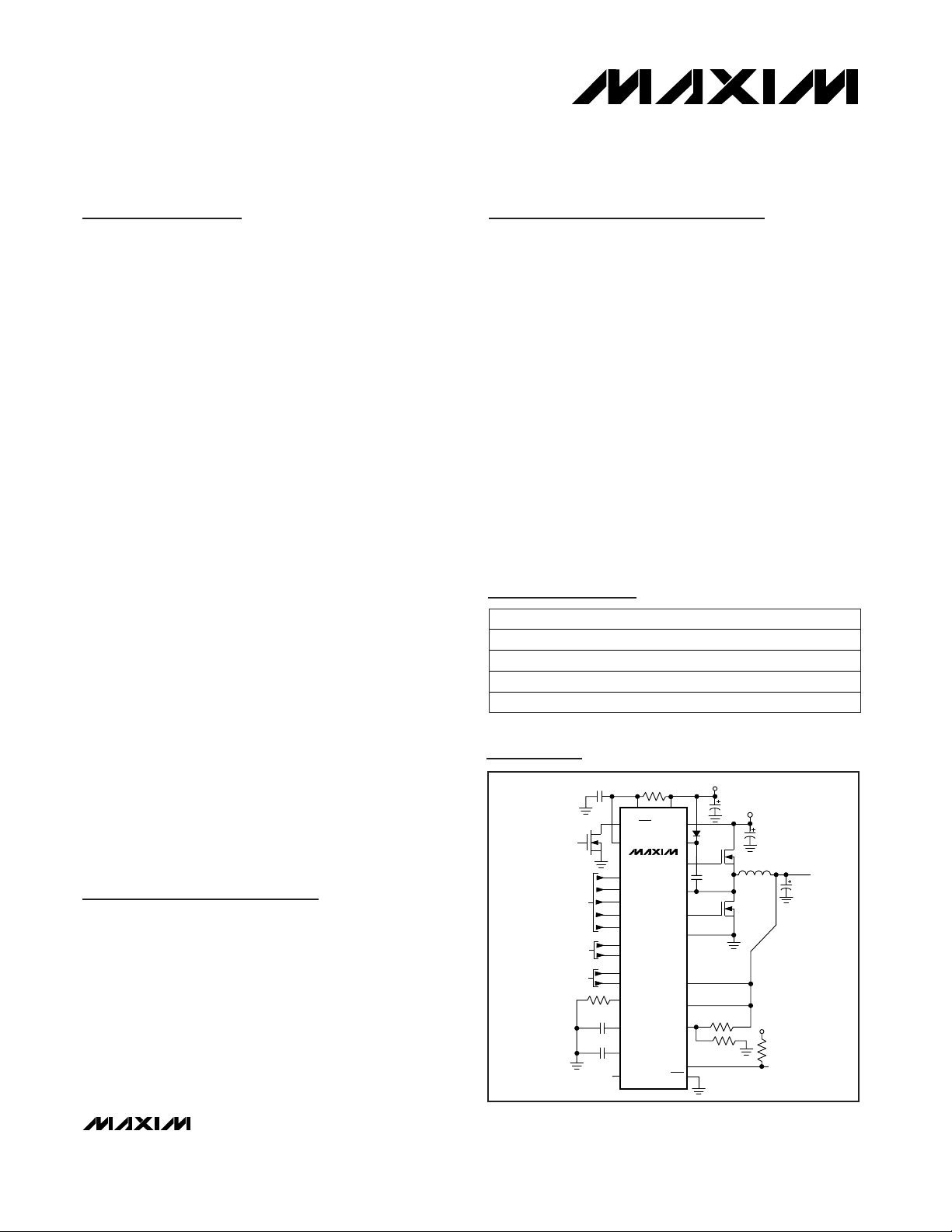
Minimal Operating Circuit
5V INPUT
BATT 2V TO 28V
V
CC
OUTPUT
0.6V TO 1.75V
POWER-GOOD
OUTPUT
SHUTDOWN
DUAL MODE VID
MUX INPUTS
MUX CONTROL
SUSPEND
INPUT
DECODER
V
CC
SKP/SDN
ILIM
MAX1718
D0
D1
D2
D3
D4
ZMODE
SUS
S0
S1
TIME
CC
REF
TON
V
DD
GND
NEG
POS
VGATE
OVP
V+
BST
DH
LX
DL
FB
MAX1718
________________________________________________________________ Maxim Integrated Products 1
For pricing, delivery, and ordering information, please contact Maxim/Dallas Direct! at
1-888-629-4642, or visit Maxim’s website at www.maxim-ic.com.
MAX1718
Notebook CPU Step-Down Controller for Intel
Mobile Voltage Positioning (IMVP-II)
2 _______________________________________________________________________________________
ABSOLUTE MAXIMUM RATINGS
ELECTRICAL CHARACTERISTICS
(Circuit of Figure 1, V+ = 15V, VCC= VDD= SKP/SDN = 5V, V
OUT
= 1.25V, TA= 0°C to +85°C, unless otherwise noted.)
Stresses beyond those listed under “Absolute Maximum Ratings” may cause permanent damage to the device. These are stress ratings only, and functional
operation of the device at these or any other conditions beyond those indicated in the operational sections of the specifications is not implied. Exposure to
absolute maximum rating conditions for extended periods may affect device reliability.
V+ to GND ..............................................................-0.3V to +30V
V
CC
, VDDto GND .....................................................-0.3V to +6V
D0–D4, ZMODE, VGATE, OVP, SUS, to GND .........-0.3V to +6V
SKP/SDN to GND ...................................................-0.3V to +16V
ILIM, CC, REF, POS, NEG, S1, S0,
TON, TIME to GND.................................-0.3V to (V
CC
+ 0.3V)
DL to GND..................................................-0.3V to (V
DD
+ 0.3V)
BST to GND ............................................................-0.3V to +36V
DH to LX .....................................................-0.3V to (BST + 0.3V)
LX to BST..................................................................-6V to +0.3V
REF Short Circuit to GND ...........................................Continuous
Continuous Power Dissipation
28-Pin QSOP (derate 10.8mW/°C above +70°C).........860mW
Operating Temperature Range ..........................-40°C to +85°C
Junction Temperature......................................................+150°C
Storage Temperature.........................................-65°C to +150°C
Lead Temperature (soldering, 10s) .................................+300°C
PARAMETER CONDITIONS MIN TYP MAX UNITS
V
228
4.5 5.5
Battery voltage, V+
VCC, V
DD
Input Voltage Range
DC Output Voltage Accuracy
V+ = 4.5V to 28V,
includes load
regulation error
DAC codes from 0.9V to 1.75V
DAC codes from 0.6V to 0.875V
-1 +1
-1.5 +1.5
%
%
Line Regulation Error VCC= 4.5V to 5.5V, V
BATT
= 4.5V to 28V
5
mV
Input Bias Current FB, POS, NEG
-0.2 +0.2
µA
V
0.4 2.5
POS, NEG Common-Mode Range
TIME Frequency Accuracy
150kHz nominal, R
TIME
= 120kΩ
380kHz nominal, R
TIME
= 47kΩ
38kHz nominal, R
TIME
= 470kΩ
V+ = 5V, FB = 1.2V, TON = GND (1000kHz)
-8 +8
-12 +12
-12 +12
230 260 290
%
ns
165 190 215
320 355 390
465 515 565
TON = REF (550kHz)
TON = open (300kHz)
TON = VCC(200kHz)
V+ = 12V, FB = 1.2V
On-Time (Note 1)
Minimum Off-Time (Note 1)
TON = VCC, open, or REF (200kHz, 300kHz, or 550kHz)
TON = GND (1000kHz)
400 500
300 375
ns
µA
700 1200
Measured at VCC, FB forced above the regulation pointQuiescent Supply Current (VCC)
Quiescent Supply Current (VDD) Measured at VDD, FB forced above the regulation point
<1 5
µA
µA
25 40
Quiescent Battery Supply
Current (V+)
Shutdown Supply Current (VCC)
Shutdown Supply Current (VDD)
SKP/SDN = GND
SKP/SDN = GND
25
<1 5
µA
µA
µA
<1 5
SKP/SDN = GND, VCC= VDD= 0V or 5V
Shutdown Battery Supply
Current (V+)
Reference Voltage VCC= 4.5V to 5.5V, no REF load
1.98 2 2.02
V
mV
-80 +80
POS - NEGPOS, NEG Differential Range
V/V
0.81 0.86 0.91
∆V
FB
/ (POS - NEG); POS - NEG = 50mVPOS, NEG Offset Gain
PWM CONTROLLER
BIAS AND REFERENCE
MAX1718
Notebook CPU Step-Down Controller for Intel
Mobile Voltage Positioning (IMVP-II)
_______________________________________________________________________________________ 3
Current-Limit Threshold Voltage
(Zero Crossing)
4
mVGND - LX
DH Gate Driver On-Resistance
1.0 3.5
ΩBST - LX forced to 5V
Current-Limit Default
Switchover Threshold
3VCC-1 VCC- 0.4 V
TA= 0°C to +85°C
85 115
TA= +25°C to +85°C
ILIM = REF (2V)
ILIM = 0.5V
PARAMETER MIN TYP MAX UNITS
Output Undervoltage Fault
Blanking Time
256
clks
Output Undervoltage Fault
Propagation Delay
10
µs
Output Undervoltage Fault
Protection Threshold
65 70 75
%
Overvoltage Fault Propagation
Delay
10
µs
Current-Limit Threshold Voltage
(Positive, Default)
90 100 110
Current-Limit Threshold Voltage
(Positive, Adjustable)
35 50 65
mV
165 200 230
REF Sink Current
Reference Load Regulation
0.01
V
10
µA
Overvoltage Trip Threshold
1.95 2.00 2.05
V
Current-Limit Threshold Voltage
(Negative)
-140 -117 -95
mV
Thermal Shutdown Threshold
150
°C
VCCUndervoltage Lockout
Threshold
4.1 4.4
V
1.0 3.5
DL Gate Driver On-Resistance
0.4 1.0
Ω
DH Gate-Driver Source/Sink
Current
1.6
A
DL Gate-Driver Sink Current
4
A
CONDITIONS
LX - GND, ILIM = V
CC
From SKP/SDN signal going high, clock speed set by R
TIME
Hysteresis = 10°C
FB forced 2% below trip threshold
With respect to unloaded output voltage
FB forced 2% above trip threshold
GND - LX, ILIM = V
CC
Rising edge, hysteresis = 20mV, PWM disabled below
this level
GND - LX
DL, high state (pullup)
DL, low state (pulldown)
DH forced to 2.5V, BST - LX forced to 5V
I
REF
= 0µA to 50µA
DL forced to 2.5V
REF in regulation
Measured at FB
mV
VGATE Lower Trip Threshold
-12 -10 -8
%Measured at FB with respect to unloaded output voltage
VGATE Upper Trip Threshold
+8 +10 +12
%Measured at FB with respect to unloaded output voltage
VGATE Propagation Delay
10
µsFB forced 2% outside VGATE trip threshold
VGATE Output Low Voltage
0.4
VI
SINK
= 1mA
VGATE Leakage Current
1
µAHigh state, forced to 5.5V
ELECTRICAL CHARACTERISTICS (continued)
(Circuit of Figure 1, V+ = 15V, VCC= VDD= SKP/SDN = 5V, V
OUT
= 1.25V, TA= 0°C to +85°C, unless otherwise noted.)
FAULT PROTECTION
GATE DRIVERS
MAX1718
Notebook CPU Step-Down Controller for Intel
Mobile Voltage Positioning (IMVP-II)
4 _______________________________________________________________________________________
ELECTRICAL CHARACTERISTICS
(Circuit of Figure 1, V+ = 15V, VCC= VDD= SKP/SDN = 5V, V
OUT
= 1.25V, TA= -40°C to +85°C, unless otherwise noted.) (Note 2)
ELECTRICAL CHARACTERISTICS (continued)
(Circuit of Figure 1, V+ = 15V, VCC= VDD= SKP/SDN = 5V, V
OUT
= 1.25V, TA= 0°C to +85°C, unless otherwise noted.)
-8 +8
-2.0 +2.0
-1.5 +1.5
MIN TYP MAX
-12 +12
-12 +12
230 290
165 215
320 390
465 565
TON = VCC(200kHz)
TON = open (300kHz)
TON = REF (550kHz)
V+ = 12V, FB = 1.2V
On-Time (Note 1)
V+ = 5V, FB = 1.2V, TON = GND (1000kHz)
38kHz nominal, R
TIME
= 470kΩ
380kHz nominal, R
TIME
= 47kΩ
150kHz nominal, R
TIME
= 120kΩ
TIME Frequency Accuracy
DAC codes from 0.6V to 0.875V
DAC codes from 0.9V to 1.75V
V+ = 4.5V to 28V,
includes load
regulation error
CONDITIONS
DC Output Voltage Accuracy
PARAMETER UNITS
%
%
ns
PWM CONTROLLER
V
SKP/SDN Float Level
I
SKP/SDN
= 0µA
1.8 2.2
PARAMETER CONDITIONS MIN TYP MAX UNITS
A
1.6
DL forced to 2.5VDL Gate-Driver Source Current
D0–D4 Pullup/Pulldown Entering impedance mode
Pullup
Pulldown
40
8
kΩ
µA
-1 +1
-1 +1
D0–D4, ZMODE = GND
ZMODE, SUS, OVP
Logic Input Current
4 Level Input Logic Levels
(TON, S0, S1)
For high
For open
For REF
For low
VCC- 0.4
3.15 3.85
1.65 2.35
0.5
V
µA
-3 +3
SKP/SDN, S0, S1, TON forced to GND or V
CC
SKP/SDN, S0, S1, and TON Input
Current
SKP/SDN Input Levels
SKP/SDN = logic high (SKIP mode)
SKP/SDN = open (PWM mode)
SKP/SDN = logic low (shutdown mode)
To enable no-fault mode
V
12 15
0.5
1.4 2.2
2.8 6
kΩ
95
D0–D4, 0 to 0.4V or 2.6V to 5.5V applied through resistor,
ZMODE = V
CC
DAC B-Mode Programming
Resistor, High
kΩ
1.05
D0–D4, 0 to 0.4V or 2.6V to 5.5V applied through resistor,
ZMODE = V
CC
DAC B-Mode Programming
Resistor, Low
V
0.8
D0–D4, ZMODE, SUS, OVP
Logic Input Low Voltage
V
2.4
D0–D4, ZMODE, SUS, OVP
Logic Input High Voltage
26
DH rising
ns
35
DL rising
Dead Time
LOGIC AND I/O
MAX1718
Notebook CPU Step-Down Controller for Intel
Mobile Voltage Positioning (IMVP-II)
_______________________________________________________________________________________ 5
ELECTRICAL CHARACTERISTICS (continued)
(Circuit of Figure 1, V+ = 15V, VCC= VDD= SKP/SDN = 5V, V
OUT
= 1.25V, TA= -40°C to +85°C, unless otherwise noted.) (Note 2)
Measured at VDD, FB forced above the regulation point µA
5
Quiescent Supply Current (VDD)
µA
40
Quiescent Battery Supply
Current (V+)
SKP/SDN = 0
SKP/SDN = 0
µA
5
Shutdown Supply Current (VDD)
µA
5
Shutdown Supply Current (VCC)
VCC= 4.5V to 5.5V, no REF load
SKP/SDN = 0, VCC= VDD= 0 or 5V
CONDITIONS
V
1.98 2.02
Reference Voltage
µA
5
Shutdown Battery Supply
Current (V+)
UNITSMIN TYP MAXPARAMETER
Measured at FB
DL, low state (pulldown)
DL, high state (pullup)
GND - LX
Rising edge, hysteresis = 20mV, PWM disabled below this
level
GND - LX, ILIM = V
CC
With respect to unloaded output voltage
LX - GND, ILIM = V
CC
Ω
1.0
3.5
DL Gate Driver On-Resistance
V
4.1 4.4
VCCUndervoltage Lockout
Threshold
mV
-145 -90
Current-Limit Threshold Voltage
(Negative)
V
1.95 2.05
Overvoltage Trip Threshold
160 240
mV
33 65
Current-Limit Threshold Voltage
(Positive, Adjustable)
mV
80 115
Current-Limit Threshold Voltage
(Positive, Default)
%
65 75
Output Undervoltage Protection
Threshold
ILIM = 0.5V
ILIM = REF (2V)
Measured at VCC, FB forced above the regulation point µA
1300
Quiescent Supply Current (VCC)
BST - LX forced to 5V Ω
3.5
DH Gate Driver On-Resistance
TON = GND (1000kHz)
ns
375
Minimum Off-Time (Note 1)
TON = VCC, open, or REF (200kHz, 300kHz, or 550kHz)
500
Measured at FB with respect to unloaded output voltage %
-12.5 -7.5
VGATE Lower Trip Threshold
Measured at FB with respect to unloaded output voltage %
+7.5 +12.5
VGATE Upper Trip Threshold
BIAS AND REFERENCE
FAULT PROTECTION
GATE DRIVERS
MAX1718
Notebook CPU Step-Down Controller for Intel
Mobile Voltage Positioning (IMVP-II)
6 _______________________________________________________________________________________
Typical Operating Characteristics
(Circuit of Figure 1, V+ = 12V, VDD= VCC= SKP/SDN = 5V, V
OUT
= 1.25V, TA= +25°C, unless otherwise noted.)
95
50-
0.01 0.1 1 10 100
EFFICIENCY vs. LOAD CURRENT
300kHz VOLTAGE POSITIONED
MAX1718 toc01
LOAD CURRENT (A)
EFFICIENCY (%)
65
75
85
80
70
60
55
90
SKIP MODE
V+ = 7V
SKIP MODE
V+ = 20V
PWM MODE
V+ = 12V
PWM MODE
V+ = 20V
SKIP MODE
V+ = 12V
PWM MODE
V+ = 7V
400
300
200
100
0
01051520
FREQUENCY vs. LOAD CURRENT
MAX1718 toc02
LOAD CURRENT (A)
FREQUENCY (kHz)
PWM MODE
SKIP MODE
250
280
270
260
290
300
310
320
330
340
350
7.0 13.810.4 17.2 20.6 24.0
FREQUENCY vs. INPUT VOLTAGE
MAX1718 toc03
INPUT VOLTAGE (V)
FREQUENCY (kHz)
I
OUT
= 18A
I
OUT
= 3A
323.0
324.0
323.5
325.0
324.5
325.5
326.0
-40 10-15 35 60 85
FREQUENCY vs. TEMPERATURE
MAX1718 toc04
TEMPERATURE (°C)
FREQUENCY (kHz)
I
OUT
= 19A
20
30
25
40
35
45
50
-40 10-15 35 60 85
OUTPUT CURRENT AT CURRENT LIMIT
vs. TEMPERATURE
MAX1718 toc05
TEMPERATURE (°C)
CURRENT (A)
0
300
200
100
400
500
600
700
800
900
1000
510152025
NO-LOAD SUPPLY CURRENT
vs. INPUT VOLTAGE
MAX1718\ toc06
INPUT VOLTAGE (V)
SUPPLY CURRENT (µA)
ICC + I
DD
I+
Note 1: On-Time specifications are measured from 50% to 50% at the DH pin, with LX forced to 0V, BST forced to 5V, and a 500pF
capacitor from DH to LX to simulate external MOSFET gate capacitance. Actual in-circuit times may be different due to
MOSFET switching speeds.
Note 2: Specifications to T
A
= -40°C are guaranteed by design and not production tested.
ELECTRICAL CHARACTERISTICS (continued)
(Circuit of Figure 1, V+ = 15V, VCC= VDD= SKP/SDN = 5V, V
OUT
= 1.25V, TA= -40°C to +85°C, unless otherwise noted.) (Note 2)
D0–D4, 0 to 0.4V or 2.6V to 5.5V applied through resistor,
ZMODE = V
CC
kΩ
95
DAC B-Mode Programming
Resistor, High
D0–D4, ZMODE, SUS, OVP
V
0.8
Logic Input Low Voltage
CONDITIONS UNITSMIN TYP MAXPARAMETER
D0–D4, 0 to 0.4V or 2.6V to 5.5V applied through resistor,
ZMODE = V
CC
kΩ
1.05
DAC B-Mode Programming
Resistor, Low
D0–D4, ZMODE, SUS, OVP
V
2.4
Logic Input High Voltage
LOGIC AND I/O
MAX1718
Notebook CPU Step-Down Controller for Intel
Mobile Voltage Positioning (IMVP-II)
_______________________________________________________________________________________ 7
0
5
10
15
20
25
30
35
40
510152025
NO-LOAD SUPPLY CURRENT
vs. INPUT VOLTAGE
MAX1718 toc07
INPUT VOLTAGE (V)
SUPPLY CURRENT (mA)
ICC + I
DD
I+
40µs/div
LOAD-TRANSIENT RESPONSE
(PWM MODE)
A
MAX1718 toc08b
B0A
A = V
OUT
, 50mV/div, AC-COUPLED
B = INDUCTOR CURRENT, 10A/div
40µs/div
LOAD-TRANSIENT RESPONSE
(SKIP MODE)
A
B
MAX1718 toc08a
0A
A = V
OUT
, 50mV/div, AC-COUPLED
B = INDUCTOR CURRENT, 10A/div
100µs/div
STARTUP WAVEFORM
(PWM MODE, NO LOAD)
A
MAX1718 toc09
B0A
A = V
OUT
, 1V/div
B = INDUCTOR CURRENT, 10A/div
C = SKP/SDN, 5V/div
C
100µs/div
STARTUP WAVEFORM
(PWM MODE, I
OUT
= 12A)
A
MAX1718 toc10
BOA
A = V
OUT
, 1V/div
B = INDUCTOR CURRENT, 10A/div
C = SKP/SDN, 5V/div
C
40µs/div
DYNAMIC OUTPUT VOLTAGE TRANSITION
(PWM MODE)
A
MAX1718 toc11
BOA
A = V
OUT
, 100mV/div, AC-COUPLED
B = INDUCTOR CURRENT, 10A/div
C = VGATE, 5V/div
D = ZMODE, 5V/div
C
D
V
OUT
= 1.15V TO 1.25V
I
OUT
= 3A, R
TIME
= 62kΩ
Typical Operating Characteristics (continued)
(Circuit of Figure 1, V+ = 12V, VDD= VCC= SKP/SDN = 5V, V
OUT
= 1.25V, TA= +25°C, unless otherwise noted.)
MAX1718
Notebook CPU Step-Down Controller for Intel
Mobile Voltage Positioning (IMVP-II)
8 _______________________________________________________________________________________
100µs/div
SHUTDOWN WAVEFORM
(PWM MODE, NO LOAD)
A
MAX1718 toc13
B0A
A = V
OUT
, 1V/div
B = INDUCTOR CURRENT, 10A/div
C = SKP/SDN, 5V/div
C
100µs/div
SHUTDOWN WAVEFORM
(PWM MODE, I
OUT
= 12A)
A
MAX1718 toc14
B0A
A = V
OUT
, 1V/div
B = INDUCTOR CURRENT, 10A/div
C = SKP/SDN, 5V/div
C
Typical Operating Characteristics (continued)
(Circuit of Figure 1, V+ = 12V, VDD= VCC= SKP/SDN = 5V, V
OUT
= 1.25V, TA= +25°C, unless otherwise noted.)
40µs/div
DYNAMIC OUTPUT VOLTAGE TRANSITION
(PWM MODE)
A
MAX1718 toc12
B0A
A = V
OUT
, 500mV/div, AC-COUPLED
B = INDUCTOR CURRENT, 10A/div
C = VGATE, 5V/div
D = SUS, 5V/div
C
D
V
OUT
= 0.7V TO 1.25V
I
OUT
= 3A, R
TIME
= 62kΩ
0.750
0.800
0.775
0.850
0.825
0.900
0.875
0.925
0.5 0.9 1.10.7 1.3 1.5 1.7 1.9
OFFSET FUNCTION SCALE FACTOR
vs. DAC SETTING
MAX1718 toc15
DAC SETTING (V)
POS-NEG SCALE FACTOR
MEASURED
THEORETICAL
1.00
1.10
1.05
1.25
1.20
1.15
1.40
1.35
1.30
1.45
-300 -100-200 0 100 200
OUTPUT VOLTAGE
vs. POS-NEG DIFFERENTIAL
MAX1718 toc16
POS-NEG (mV)
OUTPUT VOLTAGE (V)
MAX1718
Notebook CPU Step-Down Controller for Intel
Mobile Voltage Positioning (IMVP-II)
_______________________________________________________________________________________ 9
Typical Operating Characteristics (continued)
(Circuit of Figure 1, V+ = 12V, VDD= VCC= SKP/SDN = 5V, V
OUT
= 1.25V, TA= +25°C, unless otherwise noted.)
0
5
15
10
20
25
-0.48
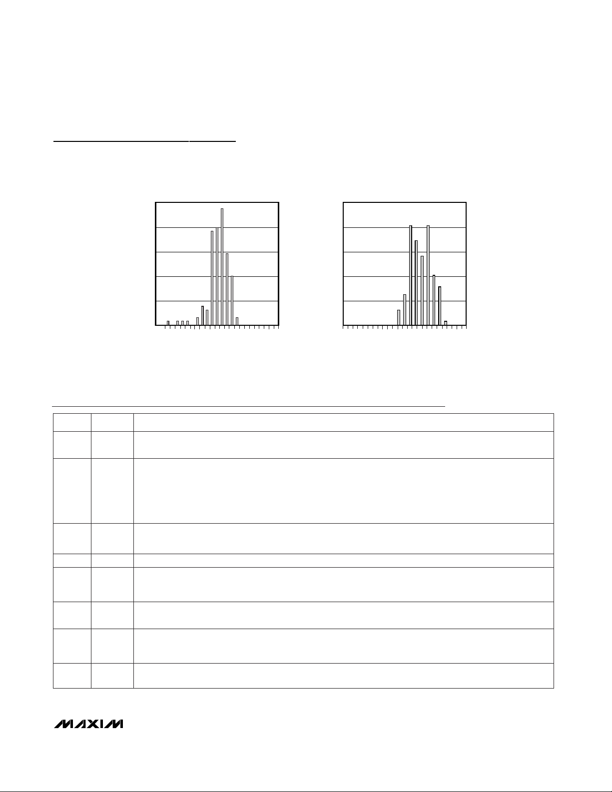
OUTPUT VOLTAGE DISTRIBUTION
MAX1718 toc17
OUTPUT VOLTAGE ERROR (%)
SAMPLE PERCENTAGE (%)
-0.24 0.480.240.00
V
OUT
= 1.25V
0
5
15
10
20
25
1.995
REFERENCE VOLTAGE DISTRIBUTION
MAX1718 toc18
REFERENCE VOLTAGE (V)
SAMPLE PERCENTAGE (%)
1.998 2.0052.0022.000
Analog Supply Voltage Input for PWM Core. Connect VCCto the system supply voltage (4.5V to 5.5V) with a
series 20Ω resistor. Bypass to GND with a 0.22µF (min) capacitor.
V
CC
9
Suspend-Mode Voltage Select Input. S0 and S1 are four-level digital inputs that select the suspend-mode
VID code for the suspend-mode multiplexer inputs. If SUS is high, the suspend-mode VID code is delivered
to the DAC (see the Internal Multiplexers (ZMODE/SUS) section).
S0, S17, 8
6 CC
Integrator Capacitor Connection. Connect a 47pF to 1000pF (47pF typ) capacitor from CC to GND to set the
integration time constant (see the Integrator Amplifiers/Output Voltage Offsets section).
Feedback Offset Adjust Negative Input. The output shifts by an amount equal to the difference between POS
and NEG multiplied by a scale factor that depends on the DAC codes (see the Integrator Amplifiers/Output
Voltage Offsets section). Connect both POS and NEG to REF if the offset function is not used.
NEG5
4 FB Feedback Input. Connect FB to the junction of the external inductor and the positioning resistor (Figure 1).
Slew-Rate Adjustment Pin. Connect a resistor from TIME to GND to set the internal slew-rate clock. A 470kΩ
to 47kΩ resistor sets the clock from 38kHz to 380kHz, f
SLEW
= 150kHz ✕120kΩ / R
TIME
.
TIME3
2
SKP/SDN
Combined Shutdown and Skip-Mode Control. Drive SKP/SDN to GND for shutdown. Leave SKP/SDN open for
low-noise forced-PWM mode, or drive to V
CC
for pulse-skipping operation. Low-noise forced-PWM mode caus-
es inductor current recirculation at light loads and suppresses pulse-skipping operation. Forcing SKP/SDN to
12V to 15V disables both the overvoltage protection and undervoltage protection circuits and clears the fault
latch, with otherwise normal pulse-skipping operation. Do not connect SKP/SDN to > 15V.
Battery Voltage Sense Connection. Connect V+ to input power source. V+ is used only for PWM one-shot
timing. DH on-time is inversely proportional to input voltage over a range of 2V to 28V.
V+1
PIN NAME FUNCTION
Pin Description
MAX1718
Notebook CPU Step-Down Controller for Intel
Mobile Voltage Positioning (IMVP-II)
10 ______________________________________________________________________________________
Pin Description (continued)
Supply Voltage Input for the DL Gate Driver, 4.5V to 5.5V. Bypass to GND with a 1µF capacitor. V
DD
17
Low-Side Gate Driver Output. DL swings GND to VDD.DL16
Analog and Power Ground. Also connects to the current-limit comparator.GND15
Open-Drain Power-Good Output. VGATE is normally high when the output is in regulation. If VFBis not within
a ±10% window of the DAC setting, VGATE is asserted low. During DAC code transitions, VGATE is forced
high until 1 clock period after the slew-rate controller finishes the transition. VGATE is low during shutdown.
VGATE14
Feedback Offset Adjust Negative Input. The output shifts by an amount equal to the difference between POS
and NEG multiplied by a scale factor that depends on the DAC codes (see the Integrator Amplifiers/Output
Voltage Offsets section). Connect both POS and NEG to REF if the offset function is not used.
POS13
Current-Limit Adjustment. The GND - LX current-limit threshold defaults to 100mV if ILIM is connected to
V
CC
. In adjustable mode, the current-limit threshold voltage is 1/10th the voltage seen at ILIM over a 0.5V to
3V range. The logic threshold for switchover to the 100mV default value is approximately V
CC
- 1V. Connect
ILIM to REF for a fixed 200mV threshold.
ILIM12
2V Reference Output. Bypass to GND with 0.22µF (min) capacitor. Can source 50µA for external loads.
Loading REF degrades FB accuracy according to the REF load-regulation error.
REF11
On-Time Selection Control Input. This is a four-level input that sets the K factor (Table 2) to determine
DH on-time. Connect TON to the following pins for the indicated operation:
GND = 1000kHz
REF = 550kHz
Open = 300kHz
VCC= 200kHz
TON10
PIN NAME FUNCTION
Suspend-Mode Control Input. When SUS is high, the suspend-mode VID code, as programmed by S0 and
S1, is delivered to the DAC. Connect SUS to GND if the Suspend-mode multiplexer is not used (see the
Internal Multiplexers (ZMODE/SUS) section).
SUS18
Performance-Mode MUX Control Input. If SUS is low, ZMODE selects between two different VID DAC codes.
If ZMODE is low, the VID DAC code is set by the logic-level voltages on D0–D4. On the rising edge of
ZMODE, during power-up with ZMODE high, or on the falling edge of SUS when ZMODE is high, the VID
DAC code is determined by the impedance at D0–D4 (see the Internal Multiplexers (ZMODE/SUS) section).
ZMODE19
Overvoltage Protection Control Input. Connect OVP low to enable overvoltage protection. Connect OVP high
to disable overvoltage protection. The overvoltage trip threshold is approximately 2V. The state of OVP does
not affect output undervoltage fault protection or thermal shutdown.
OVP
20
VID DAC Code Inputs. D0 is the LSB, and D4 is the MSB of the internal 5-bit VID DAC (Table 3). If ZMODE
is low, D0–D4 are high-impedance digital inputs, and the VID DAC code is set by the logic-level voltages on
D0–D4. On the rising edge of ZMODE, during power-up with ZMODE high, or on the falling edge of SUS
when ZMODE is high, the VID DAC code is determined by the impedance at D0–D4 as follows:
Logic low = source impedance is ≤1kΩ + 5%.
Logic high = source impedance is ≥100kΩ - 5%.
D4–D021–25
Boost Flying Capacitor Connection. Connect BST to the external boost diode and capacitor as shown in
Figure 1. An optional resistor in series with BST allows the DH pullup current to be adjusted (Figure 8).
BST26
Inductor Connection. LX is the internal lower supply rail for the DH high-side gate driver. It also connects to
the current-limit comparator and the skip-mode zero-crossing comparator.
LX27
High-Side Gate-Driver Output. DH swings LX to BST.DH28
MAX1718
Notebook CPU Step-Down Controller for Intel
Mobile Voltage Positioning (IMVP-II)
______________________________________________________________________________________ 11
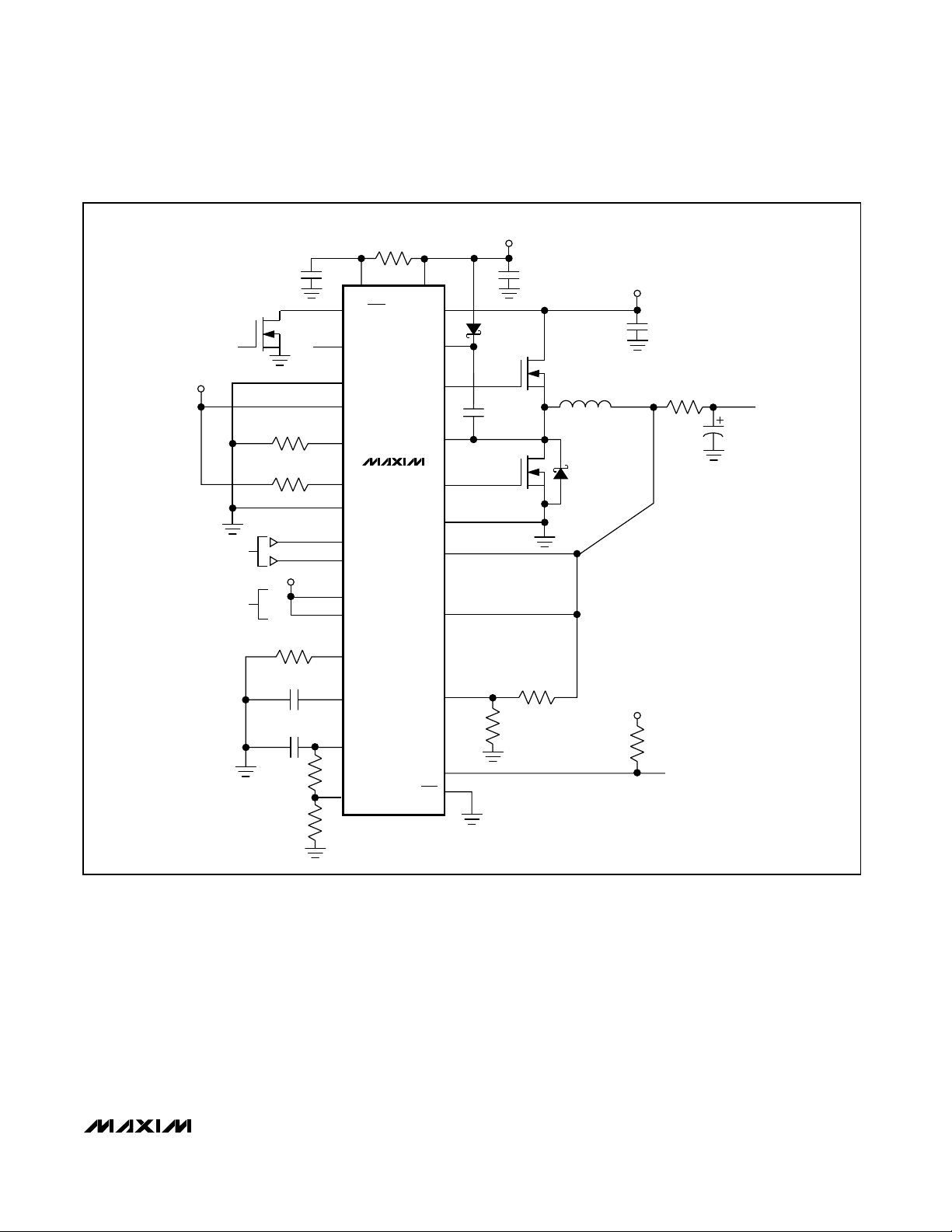
V
CC
V
CC
5V INPUT
BATT 7V TO 24V
POWER-GOOD
OUTPUT
L1
0.68µH
SKP/SDN
TON
1
10
C7
1µF
2
3
25
24
23
22
26
28
27
16
15
4
5
13
14
20
9
17
OUTPUT
0.6V TO 1.75V
D1
CMPSH-3
D2
CENTRAL
SEMICONDUCTOR
CMSH5-40
C1
1µF
C3
0.1µF
C5
0.22µF
C6
47pF
IRF7811A
Q1
FDS7764A
Q2
R5
100kΩ
2x
2x
C2, 25V, X5R
5 x 10µF
C4
6 x 270µF, 2V
PANASONIC SP
EEFUE0D271R
R1
20Ω
D0
D1
D2
SHUTDOWN
DL
LX
V+
DH
BST
GND
FB
NEG
POS
VGATE
OVP
V
DD
MAX1718
6
11
12
5V
D3
21
D4
8
S1
7
S0
18
SUS
19
MUX CONTROL
SUSPEND
INPUT
DECODER
ZMODE
TIME
CC
REF
ILIM
R4
62kΩ
R3
100kΩ
R2
100kΩ
R7
4.75kΩ
R6
511kΩ
R8
0.004Ω
REF
R19
27.4kΩ
R18
24.9kΩ
SUMIDA
CEP125#4712-TO11
Figure 1. Standard Application Circuit

MAX1718
Notebook CPU Step-Down Controller for Intel
Mobile Voltage Positioning (IMVP-II)
12 ______________________________________________________________________________________
Detailed Description
5V Bias Supply (VCCand VDD)
The MAX1718 requires an external 5V bias supply in
addition to the battery. Typically, this 5V bias supply is
the notebook’s 95% efficient 5V system supply.
Keeping the bias supply external to the IC improves
efficiency and eliminates the cost associated with the
5V linear regulator that would otherwise be needed to
supply the PWM circuit and gate drivers. If stand-alone
capability is needed, the 5V supply can be generated
with an external linear regulator.
The 5V bias supply must provide VCC(PWM controller)
and VDD(gate-drive power), so the maximum current
drawn is:
I
BIAS
= ICC+ f (QG1+ QG2) = 10mA to 40mA (typ)
where I
CC
is 800µA (typ), f is the switching frequency,
and QG1and QG2are the MOSFET data sheet total
gate-charge specification limits at VGS= 5V.
V+ and VDDcan be tied together if the input power
source is a fixed 4.5V to 5.5V supply. If the 5V bias
supply is powered up prior to the battery supply, the
enable signal (SKP/SDN going from low to high or
open) must be delayed until the battery voltage is present to ensure startup.
Free-Running, Constant On-Time PWM
Controller with Input Feed-Forward
The Quick-PWM control architecture is a pseudofixedfrequency, constant-on-time current-mode type with
voltage feed-forward (Figure 2). This architecture relies
on the output filter capacitor’s ESR to act as the current-sense resistor, so the output ripple voltage provides the PWM ramp signal. The control algorithm is
simple: the high-side switch on-time is determined solely by a one-shot whose period is inversely proportional
to input voltage and directly proportional to output voltage. Another one-shot sets a minimum off-time (400ns
typ). The on-time one-shot is triggered if the error comparator is low, the low-side switch current is below the
current-limit threshold, and the minimum off-time oneshot has timed out.
On-Time One-Shot (TON)
The heart of the PWM core is the one-shot that sets the
high-side switch on-time. This fast, low-jitter, adjustable
one-shot includes circuitry that varies the on-time in
response to battery and output voltage. The high-side
switch on-time is inversely proportional to the battery
voltage as measured by the V+ input, and proportional
to the output voltage. This algorithm results in a nearly
constant switching frequency despite the lack of a
fixed-frequency clock generator. The benefits of a constant switching frequency are twofold: first, the frequency
can be selected to avoid noise-sensitive regions such
as the 455kHz IF band; second, the inductor ripple-current operating point remains relatively constant, resulting
in easy design methodology and predictable output
voltage ripple.
On-Time = K (V
OUT
+ 0.075V) / V
IN
where K is set by the TON pin-strap connection and
0.075V is an approximation to accommodate the expected drop across the low-side MOSFET switch (Table 2).
The on-time one-shot has good accuracy at the operating
points specified in the Electrical Characteristics table
(±10% at 200kHz and 300kHz, ±12% at 550kHz and
1000kHz). On-times at operating points far removed from
the conditions specified in the Electrical Characteristics
table can vary over a wider range. For example, the
1000kHz setting will typically run about 10% slower with
inputs much greater than +5V due to the very short ontimes required.
On-times translate only roughly to switching frequencies.
The on-times guaranteed in the Electrical Character-
istics table are influenced by switching delays in the
Table 1. Component Suppliers
MANUFACTURER
USA PHONE
FACTORY FAX
Central Semiconductor
516-435-1824
Dale-Vishay
402-563-6418
Fairchild
408-721-1635
International Rectifier
310-322-3332
Kemet
408-986-1442
Motorola
602-994-6430
Nihon
847-843-2798
Panasonic
714-373-7183
Taiyo Yuden
408-573-4159
TDK
847-390-4428
Toko
408-943-9790
Sanyo
619-661-1055
SGS-Thomson
617-259-9442
Sumida
708-956-0702
Zetex
516-864-7630
516-435-1110
402-564-3131
408-721-2181
310-322-3331
408-986-0424
602-303-5454
847-843-7500
714-373-7939
408-573-4150
847-390-4373
800-745-8656
619-661-6835
617-259-0300
708-956-0666
516-543-7100

MAX1718
Notebook CPU Step-Down Controller for Intel
Mobile Voltage Positioning (IMVP-II)
______________________________________________________________________________________ 13
REF
-10%
FROM
D/A
REF
REF
FB
OVP
ZMODE
TIME
10k
ERROR
AMP
TOFF
TON
REF
+10%
NEG
R-2R
D/A CONVERTER
CHIP SUPPLY
g
m
g
m
CC
POS
VGATE
D0 D1 D2 D3
S1SUS
S0 D4
ON-TIME
COMPUTE
TON
1-SHOT
1-SHOT
TRIG
V
BATT
2V TO 28V
TRIG
Q
Q
S
R
2V
REF
REF
FB
GND
5V
OUTPUT
DL
V
CC
V
DD
LX
ZERO CROSSING
CURRENT
LIMIT
DH
BST
I
LIM
REF
5V
5V
Q
OVP/UVP
DETECT
SKP/SDN
TON
V+
70kΩ
Σ
MAX1718
S
R
Q
MUXES AND SLEW CONTROL
9
1
Figure 2. Functional Diagram

MAX1718
Notebook CPU Step-Down Controller for Intel
Mobile Voltage Positioning (IMVP-II)
14 ______________________________________________________________________________________
external high-side MOSFET. Resistive losses, including
the inductor, both MOSFETs, output capacitor ESR, and
PC board copper losses in the output and ground tend
to raise the switching frequency at higher output currents. Also, the dead-time effect increases the effective
on-time, reducing the switching frequency. It occurs
only in PWM mode (SKP/SDN = open) and during
dynamic output voltage transitions when the inductor
current reverses at light or negative load currents. With
reversed inductor current, the inductor’s EMF causes
LX to go high earlier than normal, extending the on-time
by a period equal to the DH-rising dead time.
For loads above the critical conduction point, where the
dead-time effect is no longer a factor, the actual switching
frequency is:
where V
DROP1
is the sum of the parasitic voltage drops
in the inductor discharge path, including synchronous
rectifier, inductor, and PC board resistances; V
DROP2
is
the sum of the parasitic voltage drops in the inductor
charge path, including high-side switch, inductor, and
PC board resistances; and tONis the on-time calculated by the MAX1718.
Integrator Amplifiers/Output
Voltage Offsets
Two transconductance integrator amplifiers provide a
fine adjustment to the output regulation point. One
amplifier forces the DC average of the feedback voltage to equal the VID DAC setting. The second amplifier
is used to create small positive or negative offsets from
the VID DAC setting, using the POS and NEG pins.
The integrator block has the ability to lower the output
voltage by 8% and raise it by 8%. For each amplifier,
the differential input voltage range is at least ±80mV
total, including DC offset and AC ripple. The two amplifiers’ outputs are directly summed inside the chip, so
the integration time constant can be set easily with one
capacitor at the CC pin. Use a capacitor value of 47pF
to 1000pF (47pF typ). The g
m
of each amplifier is
160µmho (typ).
The POS/NEG amplifier is used to add small offsets to
the VID DAC setting or to correct for voltage drops. To
create an output offset, bias POS and NEG to a voltage
(typically V
OUT
or REF) within their common-mode
range, and offset them from one another with a resistive
divider (Figures 3 and 4). If V
POS
is higher than V
NEG
,
then the output is shifted in the positive direction. If
V
NEG
is higher than V
POS
, then the output is shifted in
the negative direction. The amount of output offset is
less than the difference from POS to NEG by a scale
factor that varies with the VID DAC setting as shown in
Table 3. The common-mode range of POS and NEG is
0.4V to 2.5V.
For applications that require multiple offsets, an external multiplexer can be used to select various resistor
values (Figure 5).
Both the integrator amplifiers can be disabled by connecting NEG to VCC.
Forced-PWM Mode (SKP/
SDN
Open)
The low-noise forced-PWM mode (SKP/SDN open) disables the zero-crossing comparator, allowing the inductor current to reverse at light loads. This causes the
low-side gate-drive waveform to become the complement of the high-side gate-drive waveform. The benefit
of forced-PWM mode is to keep the switching frequency fairly constant, but it comes at a cost: the no-load
battery current can be 10mA to 40mA, depending on
the external MOSFETs and switching frequency.
Forced-PWM mode is required during downward output
voltage transitions. The MAX1718 uses PWM mode during all transitions, but only while the slew-rate controller
is active. Due to voltage positioning, when a transition
uses high negative inductor current, the output voltage
does not settle to its final intended value until well after
the slew-rate controller terminates. Because of this it is
possible, at very high negative slew currents, for the output to end up high enough to cause VGATE to go low.
f
VV
tVV V
OUT DROP
ON IN DROP DROP
=
+
+−
()
()
1
12
Table 2. Approximate K-Factor Errors
MIN RECOMMENDED V
BATT
AT
TON
SETTING
TON
FREQUENCY
(kHZ)
K-FACTOR
(µs)
APPROXIMATE K-
FACTOR ERROR (%)
V
OUT
= 1.25V (V) V
OUT
= 1.75V (V)
V
CC
200 5
±10
1.7
2.3
OPEN 300 3.3 ±10 1.8 2.5
REF 550 1.8 ±12.5 2.6 3.5
GND 1000 1.0 ±12.5 3.6 4.9

MAX1718
Notebook CPU Step-Down Controller for Intel
Mobile Voltage Positioning (IMVP-II)
______________________________________________________________________________________ 15
Thus, it is necessary to use forced PWM mode during all
negative transitions. Most applications should use PWM
mode exclusively, although there is some benefit to
using skip mode while in the low-power suspend state
(see the Using Skip Mode During Suspend (SKP/
SDN
=
VCC) section.)
Automatic Pulse-Skipping Switchover
In skip mode (SKP/SDN high), an inherent automatic
switchover to PFM takes place at light loads (Figure 6).
This switchover is effected by a comparator that truncates the low-side switch on-time at the inductor current’s
zero crossing. This mechanism causes the threshold
between pulse-skipping PFM and nonskipping PWM
operation to coincide with the boundary between continuous and discontinuous inductor-current operation.
The load-current level at which PFM/PWM crossover
occurs, I
LOAD(SKIP)
, is equal to 1/2 the peak-to-peak
ripple current, which is a function of the inductor value
(Figure 6). For a battery range of 7V to 24V, this threshold is relatively constant, with only a minor dependence
on battery voltage:
where K is the on-time scale factor (Table 2). For example, in the standard application circuit this becomes:
The crossover point occurs at a lower value if a swinging (soft-saturation) inductor is used.
The switching waveforms may appear noisy and asynchronous when light loading causes pulse-skipping
operation, but this is a normal operating condition that
results in high light-load efficiency. Trade-offs in PFM
noise vs. light-load efficiency are made by varying the
inductor value. Generally, low inductor values produce
a broader efficiency vs. load curve, while higher values
result in higher full-load efficiency (assuming that the
coil resistance remains fixed) and less output voltage
ripple. Penalties for using higher inductor values
include larger physical size and degraded load-transient response, especially at low input voltage levels.
Current-Limit Circuit
The current-limit circuit employs a unique “valley” currentsensing algorithm that uses the on-resistance of the
low-side MOSFET as a current-sensing element. If the
current-sense signal is above the current-limit threshold, the PWM is not allowed to initiate a new cycle
33 125
2068
12 1 25
12
27
. .
.
.
.
µµsVHVV
V
A
×
×
×
−
=
I
KV
L
VV
V
LOAD SKIP
OUT BATT OUT
BATT
()
≈
×
×
×
−
2
REF
MAX1718
POS
NEG
Figure 3. Resistive Divider from REF
DL
DH
MAX1718
POS
NEG
Figure 4. Resistive Divider from OUTPUT
DL
DH
B
A
MAX1718
SEL
MUX
POS
NEG
MAX4524
Figure 5. Programmable Offset Voltage

MAX1718
Notebook CPU Step-Down Controller for Intel
Mobile Voltage Positioning (IMVP-II)
16 ______________________________________________________________________________________
(Figure 7). The actual peak current is greater than the
current-limit threshold by an amount equal to the inductor ripple current. Therefore, the exact current-limit
characteristic and maximum load capability are a function of the MOSFET on-resistance, inductor value, and
battery voltage. The reward for this uncertainty is
robust, lossless overcurrent sensing. When combined
with the undervoltage protection circuit, this currentlimit method is effective in almost every circumstance.
There is also a negative current limit that prevents
excessive reverse inductor currents when V
OUT
is sinking
current. The negative current-limit threshold is set to
approximately 120% of the positive current limit, and
therefore tracks the positive current limit when ILIM is
adjusted.
The current-limit threshold is adjusted with an external
resistor-divider at ILIM. The current-limit threshold voltage adjustment range is from 50mV to 300mV. In the
adjustable mode, the current-limit threshold voltage is
precisely 1/10th the voltage seen at ILIM. The threshold
defaults to 100mV when ILIM is connected to VCC. The
logic threshold for switchover to the 100mV default
value is approximately VCC- 1V.
The adjustable current limit accommodates MOSFETs
with a wide range of on-resistance characteristics (see
the Design Procedure section). For a high-accuracy
current-limit application, see Figure 16.
Carefully observe the PC board layout guidelines to
ensure that noise and DC errors don’t corrupt the currentsense signals seen by LX and GND. Place the IC close
to the low-side MOSFET with short, direct traces, making a Kelvin sense connection to the source and drain
terminals.
MOSFET Gate Drivers (DH, DL)
The DH and DL drivers are optimized for driving moderate-sized high-side and larger low-side power
MOSFETs. This is consistent with the low duty factor
seen in the notebook CPU environment, where a large
V
BATT
- V
OUT
differential exists. An adaptive dead-time
circuit monitors the DL output and prevents the highside FET from turning on until DL is fully off. There must
be a low-resistance, low-inductance path from the DL
driver to the MOSFET gate for the adaptive dead-time circuit to work properly. Otherwise, the sense circuitry in the
MAX1718 will interpret the MOSFET gate as “off” while
there is actually still charge left on the gate. Use very
short, wide traces measuring 10 to 20 squares (50 to 100
mils wide if the MOSFET is 1 inch from the MAX1718).
The dead time at the other edge (DH turning off) is
determined by a fixed 35ns (typ) internal delay.
The internal pulldown transistor that drives DL low is
robust, with a 0.4Ω (typ) on-resistance. This helps pre-
vent DL from being pulled up during the fast rise-time
of the inductor node, due to capacitive coupling from
the drain to the gate of the low-side synchronous-rectifier MOSFET. However, for high-current applications, you
might still encounter some combinations of high- and
low-side FETs that will cause excessive gate-drain coupling, which can lead to efficiency-killing, EMIproducing shoot-through currents. This is often remedied
by adding a resistor in series with BST, which increases
the turn-on time of the high-side FET without degrading
the turn-off time (Figure 8).
POR
Power-on reset (POR) occurs when VCCrises above
approximately 2V, resetting the fault latch and preparing
the PWM for operation. VCCundervoltage lockout
INDUCTOR CURRENT
I
LOAD
= I
PEAK
/2
ON-TIME0 TIME
I
PEAK
L
V
BATT
- V
OUT
∆i
∆t
=
Figure 6. Pulse-Skipping/Discontinuous Crossover Point
INDUCTOR CURRENT
I
LIMIT
I
LOAD
0 TIME
I
PEAK
Figure 7. “Valley” Current-Limit Threshold Point

MAX1718
Notebook CPU Step-Down Controller for Intel
Mobile Voltage Positioning (IMVP-II)
______________________________________________________________________________________ 17
(UVLO) circuitry inhibits switching, forces VGATE low,
and forces the DL gate driver high (to enforce output
overvoltage protection). When VCCrises above 4.2V, the
DAC inputs are sampled and the output voltage begins
to slew to the DAC setting.
For automatic startup, the battery voltage should be
present before VCC. If the MAX1718 attempts to bring
the output into regulation without the battery voltage
present, the fault latch will trip. The SKP/SDN pin can
be toggled to reset the fault latch.
Shutdown
When SKP/SDN goes low, the MAX1718 enters lowpower shutdown mode. VGATE goes low immediately.
The output voltage ramps down to 0V in 25mV steps at
the clock rate set by R
TIME
. When the DAC reaches the
0V setting, DL goes high, DH goes low, the reference is
turned off, and the supply current drops to about 2µA.
When SKP/SDN goes high or floats, the reference powers up, and after the reference UVLO is passed, the
DAC target is evaluated and switching begins. The
slew-rate controller ramps up from 0V in 25mV steps to
the currently selected code value (based on ZMODE
and SUS). There is no traditional soft-start (variable current limit) circuitry, so full output current is available
immediately. VGATE goes high after the slew-rate controller has terminated and the output voltage is in regulation.
UVLO
If VCCdrops low enough to trip the UVLO comparator, it
is assumed that there is not enough supply voltage to
make valid decisions. To protect the output from overvoltage faults, DL is forced high in this mode. This will
force the output to GND, but it will not use the slew-rate
controller. This results in large negative inductor current
and possibly small negative output voltages. If V
CC
is
likely to drop in this fashion, the output can be clamped
with a Schottky diode to GND to reduce the negative
excursion.
DAC Inputs D0–D4
The digital-to-analog converter (DAC) programs the
output voltage. It typically receives a preset digital code
from the CPU pins, which are either hard-wired to GND
or left open-circuit. They can also be driven by digital
logic, general-purpose I/O, or an external mux. Do not
leave D0–D4 floating—use 1MΩ or less pullups if the
inputs may float. D0–D4 can be changed while the
SMPS is active, initiating a transition to a new output
voltage level. If this mode of DAC control is used, connect
ZMODE and SUS low. Change D0–D4 together, avoiding greater than 1µs skew between bits. Otherwise,
incorrect DAC readings may cause a partial transition to
the wrong voltage level, followed by the intended transition to the correct voltage level, lengthening the overall
transition time. The available DAC codes and resulting
output voltages (Table 3) are compatible with IMVP-II
specification.
Internal Multiplexers (ZMODE, SUS)
The MAX1718 has two unique internal VID input multiplexers (muxes) that can select one of three different
VID DAC code settings for different processor states.
Depending on the logic level at SUS, the Suspend
(SUS) mode mux selects the VID DAC code settings
from either the ZMODE mux or the S0/S1 input decoder.
The ZMODE mux selects one of the two VID DAC code
settings from the D0–D4 pins, based on either voltage
on the pins or the output of the impedance decoder
(Figure 9).
When SUS is high, the Suspend mode mux selects the
VID DAC code settings from the S0/S1 input decoder.
The outputs of the decoder are determined by inputs
S0 and S1 (Table 4).
When SUS is low, the Suspend mode mux selects the
output of the ZMODE mux. Depending on the logic level
at ZMODE, the ZMODE mux selects the VID DAC code
settings using either the voltage on D0–D4 or the output
of the impedance decoder (Table 5).
If ZMODE is low, the logic-level voltages on D0–D4 set
the VID DAC settings. This is called Logic mode. In this
mode, the inputs are continuously active and can be
dynamically changed by external logic. The Logic
mode VID DAC code setting is typically used for the
Battery mode state, and the source of this code is
sometimes the VID pins of the CPU with suitable pullup
resistors.
BST
+5V
V
BATT
5Ω TYP
DH
LX
MAX1718
Figure 8. Reducing the Switching-Node Rise Time

MAX1718
Notebook CPU Step-Down Controller for Intel
Mobile Voltage Positioning (IMVP-II)
18 ______________________________________________________________________________________
Table 3. Output Voltage vs. DAC Codes
D4 D3 D2 D1 D0
OUTPUT
VOLTAGE (V)
POS/NEG SCALE
FACTOR
00000 1.75 0.90
00001 1.70 0.90
00010 1.65 0.90
00011 1.60 0.89
00100 1.55 0.89
00101 1.50 0.89
00110 1.45 0.88
00111 1.40 0.88
01000 1.35 0.88
01001 1.30 0.87
01010 1.25 0.87
01011 1.20 0.86
01100 1.15 0.86
01101 1.10 0.85
01110 1.05 0.85
01111 1.00 0.84
10000 0.975 0.84
10001 0.950 0.83
10010 0.925 0.83
10011 0.900 0.82
10100 0.875 0.82
10101 0.850 0.82
10110 0.825 0.81
10111 0.800 0.81
11000 0.775 0.80
11001 0.750 0.80
11010 0.725 0.79
11011 0.700 0.78
11100 0.675 0.78
11101 0.650 0.77
11110 0.625 0.76
11111 0.600 0.76

MAX1718
Notebook CPU Step-Down Controller for Intel
Mobile Voltage Positioning (IMVP-II)
______________________________________________________________________________________ 19
On the rising edge of ZMODE, during power-up with
ZMODE high or on the falling edge of SUS when
ZMODE is high, the impedances at D0–D4 are sampled
by the impedance decoder to see if a large resistance
is in series with the pin. This is called Impedance
mode. If the voltage level on the pin is a logic low, an
internal switch connects the pin to an internal 26kΩ
pullup for about 4µs to see if the pin voltage can be
forced high (Figure 10). If the pin voltage can be pulled
to a logic high, the impedance is considered high and
so is the Impedance mode logic state. Similarly, if the
voltage level on the pin is a logic high, an internal
switch connects the pin to an internal 8kΩ pulldown to
see if the pin voltage can be forced low. If so, the pin is
high impedance and its Impedance mode logic state is
high. In either sampling condition, if the pin’s logic level
does not change, the pin is determined to be low
impedance and the Impedance mode logic state is low.
A high pin impedance (and logic high) is 100kΩ or
greater, and a low impedance (and logic low) is 1kΩ or
less. The Electrical Characteristics table guaranteed
levels for these impedances are 95kΩ and 1.05kΩ to
allow the use of standard 100kΩ and 1kΩ resistors with
5% tolerance.
Using the ZMODE Mux
There are many ways to use the versatile ZMODE mux.
The preferred method will depend on when and how
the VID DAC codes for the various states are determined. If the output voltage codes are fixed at PC
board design time, program both codes with a simple
combination of pin-strap connections and series resistors (Figure 11). If the output voltage codes are chosen
during PC board assembly, both codes can be independently programmed with resistors (Figure 12). This
matrix of 10 resistor-footprints can be programmed to
all possible Logic mode and Impedance mode code
combinations with only 5 resistors.
Often the CPU pins provide one set of codes that are
typically used with pullup resistors to provide the Logic
mode VID code, and resistors in series with D0–D4 set
the Impedance mode code. Since some of the CPU’s
VID pins may float, the open-circuit pins can present a
problem for the ZMODE mux’s Impedance mode. For
the Impedance mode to work, any pins intended to be
S1 S0
OUTPUT VOLTAGE (V)
GND GND 0.975
GND REF 0.950
GND OPEN 0.925
GND V
CC
0.900
REF GND 0.875
REF REF 0.850
REF OPEN 0.825
REF V
CC
0.800
OPEN GND 0.775
OPEN REF 0.750
OPEN OPEN 0.725
OPEN V
CC
0.700
V
CC
GND 0.675
V
CC
REF 0.650
V
CC
OPEN 0.625
V
CC
V
CC
0.600
Table 4. Suspend Mode DAC Codes
D0
D1
D2
D3
D4
ZMODE
VCC POR
ZMODE MUX
S0/S1
DECODER
SEL
OUT
OUT
1
IN
IMPEDANCE
DECODER
IN
0
SUS MUX
SEL
OUT
DAC
1
0
S0
S1
SUS
Figure 9. Internal Multiplexers Functional Diagram

MAX1718
Notebook CPU Step-Down Controller for Intel
Mobile Voltage Positioning (IMVP-II)
20 ______________________________________________________________________________________
low during Impedance mode must appear to be low
impedance, at least for the 4µs sampling interval.
This can be achieved in several ways, including the following two (Figure 13). By using low-impedance pullup
resistors with the CPU’s VID pins, each pin provides the
low impedance needed for the mux to correctly interpret the Impedance mode setting. Unfortunately, the
low resistances cause several mA quiescent currents
for each of the CPU’s grounded VID pins. This quiescent current can be avoided by taking advantage of the
fact that D0–D4 need only appear low impedance
briefly, not necessarily on a continuous DC basis. Highimpedance pullups can be used if they are bypassed
with a large enough capacitance to make them appear
low impedance for the 4µs sampling interval. As noted
in Figure 13, 4.7nF capacitors allow the inputs to
appear low impedance even though they are pulled up
with large-value resistors. Each sampling depletes
some charge from the 4.7nF capacitors. A minimum
26kΩ
D4
D3
D2
D1
D0
26kΩ 26kΩ 26kΩ 26kΩ
8kΩ
100kΩ
8kΩ 8kΩ 8kΩ 8kΩ
3.0V TO 5.5V
100kΩ
+5V
B-DATA
LATCH
V
CC
GND
MAX1718
Figure 10. Internal Mux Impedance-Mode Data Test and Latch
MAX1718
D4
D3
D2
D1
D0
ZMODE
3.0V TO 5.5V
ZMODE HIGH
VID = 01010
1.25V
ZMODE LOW
VID = 01100
1.15V
100kΩ
100kΩ
ZMODE = HIGH = 1.25V
ZMODE = LOW = 1.15V
Figure 11. Using the Internal Mux with Hard-Wired Logic-Mode
and Impedance-Mode DAC Codes

MAX1718
Notebook CPU Step-Down Controller for Intel
Mobile Voltage Positioning (IMVP-II)
______________________________________________________________________________________ 21
interval of 2 ✕R
PULLUP
✕
4.7nF is recommended
between ZMODE samples.
In some cases, it is desirable to determine the
Impedance mode code during system boot so that several processor types can be used without hardware
modifications. Figure 14 shows one way to implement
this function. The desired code is determined by the
system BIOS and programmed into one register of the
MAX1609 using the SMBus™ serial interface. The
MAX1609’s other register is left in its power-up state (all
outputs high impedance). When SMBSUS is low, the
outputs are high impedance and do not affect the
Logic-mode VID code setting. When SMBSUS is high,
the programmed register is selected, and the MAX1609
forces a low impedance on the appropriate VID input
pins. The ZMODE signal is delayed relative to the SMB-
SUS pin because the VID pins that are pulled low by
the MAX1609 take significant time to rise when they are
released. One additional benefit of using the MAX1609
for this application is that the application uses only five of
the MAX1609’s high-voltage, open-drain outputs. The
other three outputs can be used for other purposes.
Output Voltage Transition Timing
The MAX1718 is designed to perform output voltage
transitions in a controlled manner, automatically minimizing input surge currents. This feature allows the circuit designer to achieve nearly ideal transitions,
guaranteeing just-in-time arrival at the new output voltage level with the lowest possible peak currents for a
given output capacitance. This makes the IC ideal for
IMVP-II CPUs.
IMVP-II CPUs operate at two distinct clock frequencies
and require three distinct VID settings. When transitioning from one clock frequency to the other, the CPU first
goes into a low-power state, then the output voltage
and clock frequency are changed. The change must
be accomplished in 100µs or the system may halt.
MAX1718
D4
D3
D2
D1
D0
ZMODE
ZMODE = HIGH = 1.25V
ZMODE = LOW = 1.15V
1kΩ
1kΩ100kΩ
1kΩ
100kΩ
2.7V TO 5.5V
NOTE: USE PULLUP FOR LOGIC MODE 1, PULLDOWN FOR LOGIC MODE 0.
USE ≥100kΩ FOR IMPEDANCE MODE 1, ≤1kΩ FOR IMPEDANCE MODE 0.
Figure 12. Using the Internal Mux with Both VID Codes Resistor Programmed
ZMODE SUS
OUTPUT VOLTAGE
DETERMINED BY:
GND GND Logic Level of D0–D4
V
CC
GND Impedance of D0–D4
XVCCLogic Levels of S0, S1
Table 5. DAC Mux Operation
SMBus™ is a trademark of Intel Corp.

MAX1718
Notebook CPU Step-Down Controller for Intel
Mobile Voltage Positioning (IMVP-II)
22 ______________________________________________________________________________________
At the beginning of an output voltage transition, the
MAX1718 blanks the VGATE output, preventing it from
going low. VGATE remains blanked during the transition and is re-enabled when the slew-rate controller has
set the internal DAC to the final value and one additional slew-rate clock period has passed. The slew-rate
clock frequency (set by resistor R
TIME
) must be set fast
enough to ensure that the longest required transition is
completed within the allowed 100µs.
The output voltage transition is performed in 25mV
steps, preceded by a delay and followed by one additional clock period. The total time for a transition
depends on R
TIME
, the voltage difference, and the
accuracy of the MAX1718’s slew-rate clock, and is not
dependent on the total output capacitance. The greater
the output capacitance, the higher the surge current
required for the transition. The MAX1718 will automatically control the current to the minimum level required
to complete the transition in the calculated time, as long
as the surge current is less than the current limit set by
ILIM. The transition time is given by:
where f
SLEW
= 150kHz ✕120kΩ / R
TIME
, V
OLD
is the
original DAC setting, V
NEW
is the new DAC setting, and
T
DELAY
ranges from zero to a maximum of 2/f
SLEW
. See
Time Frequency Accuracy in the Electrical Charac-
teristics table for f
SLEW
accuracy.
The practical range of R
TIME
is 47kΩ to 470kΩ, corre-
sponding to 2.6µs to 26µs per 25mV step. Although the
DAC takes discrete 25mV steps, the output filter makes
the transitions relatively smooth. The average inductor
current required to make an output voltage transition is:
I
L
≅ C
OUT
✕ 25mV ✕ f
SLEW
Output Overvoltage Protection
The overvoltage protection (OVP) circuit is designed to
protect the CPU against a shorted high-side MOSFET
by drawing high current and blowing the battery fuse.
The output voltage is continuously monitored for over-
≤×
−
+
1
25f
VV
mV
T
SLEW
OLD NEW
DELAY
MAX1718
D4
D3
D2
D1
D0
ZMODE
*TO REDUCE QUIESCENT CURRENT, 1kΩ PULLUP RESISTORS CAN BE REPLACED BY 1MΩ RESISTORS WITH 4.7nF CAPACATORS IN PARALLEL.
ZMODE HIGH
VID = 01010 → 1.25V
CPU VID =
01100 → 1.15V
(ZMODE LOW)
1kΩ
1MΩ
1kΩ 1kΩ 1kΩ 1kΩ
4.7nF
*OPTIONAL
3.15V TO 5.5V
100kΩ
100kΩ
CPU
ZMODE = HIGH = 1.25V
ZMODE = LOW = 1.15V
Figure 13. Using the Internal Mux with CPU Driving the Logic-Mode VID Code

MAX1718
Notebook CPU Step-Down Controller for Intel
Mobile Voltage Positioning (IMVP-II)
______________________________________________________________________________________ 23
voltage. If the output is more than 2V, OVP is triggered
and the circuit shuts down. The DL low-side gate-driver
output is then latched high until SKP/SDN is toggled or
VCCpower is cycled below 1V. This action turns on the
synchronous-rectifier MOSFET with 100% duty and, in
turn, rapidly discharges the output filter capacitor and
forces the output to ground. If the condition that caused
the overvoltage (such as a shorted high-side MOSFET)
persists, the battery fuse will blow. DL is also kept high
continuously when VCCUVLO is active, as well as in
shutdown mode (Table 6).
Overvoltage protection can be defeated with a logic
high on OVP or through the NO FAULT test mode (see
the NO FAULT Test Mode section).
Output Undervoltage Shutdown
The output UVP function is similar to foldback current
limiting, but employs a timer rather than a variable current limit. If the MAX1718 output voltage is under 70% of
the nominal value, the PWM is latched off and won’t
restart until VCCpower is cycled or SKP/SDN is toggled. To allow startup, UVP is ignored during the undervoltage fault-blanking time (the first 256 cycles of the
slew rate after startup).
UVP can be defeated through the NO FAULT test mode
(see the NO FAULT Test Mode section).
3.3V
R = 100kΩRRRR
VID4
VID3
VID2
VID1
VID0
1nF
GMUXSEL
SMBSUS
ADDRESS
SMBUS
DATA
CLOCK
ADD0
ADD1
0
1
0
1
0
1
1
1
1
1
3.3kΩ
ZMODE
CPU
MAX1718
3.3V
MAX1609
R
R
R
R
R
Figure 14. Using the ZMODE Multiplexer

MAX1718
Notebook CPU Step-Down Controller for Intel
Mobile Voltage Positioning (IMVP-II)
24 ______________________________________________________________________________________
NO FAULT Test Mode
The over/undervoltage protection features can complicate the process of debugging prototype breadboards
since there are (at most) a few milliseconds in which to
determine what went wrong. Therefore, a test mode is
provided to disable the OVP, UVP, and thermal shutdown features, and clear the fault latch if it has been
set. The PWM operates as if SKP/SDN were high (SKIP
mode). The NO FAULT test mode is entered by forcing
12V to 15V on SKP/SDN.
Design Procedure
Firmly establish the input voltage range and maximum
load current before choosing a switching frequency
and inductor operating point (ripple-current ratio). The
primary design trade-off lies in choosing a good switching frequency and inductor operating point, and the following four factors dictate the rest of the design:
1) Input Voltage Range. The maximum value (V
IN(MAX)
)
must accommodate the worst-case high AC adapter
voltage. The minimum value (V
IN(MIN)
) must account
for the lowest battery voltage after drops due to connectors, fuses, and battery selector switches. If there
is a choice at all, lower input voltages result in better
efficiency.
2) Maximum Load Current. There are two values to con-
sider. The peak load current (I
LOAD(MAX)
) determines the instantaneous component stresses and
filtering requirements, and thus drives output capacitor selection, inductor saturation rating, and the
design of the current-limit circuit. The continuous load
current (I
LOAD
) determines the thermal stresses and
thus drives the selection of input capacitors,
MOSFETs, and other critical heat-contributing components. Modern notebook CPUs generally exhibit
I
LOAD
= I
LOAD(MAX)
✕
80%.
3) Switching Frequency. This choice determines the
basic trade-off between size and efficiency. The optimal frequency is largely a function of maximum input
voltage, due to MOSFET switching losses that are proportional to frequency and V
IN
2
. The optimum frequency is also a moving target, due to rapid improvements
in MOSFET technology that are making higher frequencies more practical.
4) Inductor Operating Point. This choice provides trade-
offs between size and efficiency. Low inductor values cause large ripple currents, resulting in the
smallest size, but poor efficiency and high output
noise. The minimum practical inductor value is one
that causes the circuit to operate at the edge of critical conduction (where the inductor current just touches zero with every cycle at maximum load). Inductor
values lower than this grant no further size-reduction
benefit.
The MAX1718’s pulse-skipping algorithm initiates
skip mode at the critical conduction point. So, the
inductor operating point also determines the loadcurrent value at which PFM/PWM switchover occurs.
The optimum point is usually found between 20%
and 50% ripple current.
5) The inductor ripple current also impacts transientresponse performance, especially at low VIN- V
OUT
differentials. Low inductor values allow the inductor
current to slew faster, replenishing charge removed
from the output filter capacitors by a sudden load
SKP/SDN
DL MODE COMMENT
GND High Shutdown
Low-power shutdown state. DL is forced to VDD, enforcing
OVP. ICC+ IDD= 2µA typ.
12V to 15V Switching No Fault
Test mode with faults disabled and fault latches cleared, including thermal shutdown. Otherwise, normal operation, with automatic PWM/PFM switchover for pulse-skipping at light loads.
Open Switching Run (PWM, low noise)
Low-noise operation with no automatic switchover. Fixed-frequency PWM action is forced regardless of load. Inductor current reverses at light load levels.
V
CC
Switching Run (PFM/PWM)
Operation with automatic PWM/PFM switchover for pulse-skipping at light loads.
VCCor Open High Fault
Fault latch has been set by OVP, UVP, or thermal shutdown.
Device will remain in FAULT mode until VCCpower is cycled or
SKP/SDN is forced low.
Table 6. Operating Mode Truth Table

MAX1718
Notebook CPU Step-Down Controller for Intel
Mobile Voltage Positioning (IMVP-II)
______________________________________________________________________________________ 25
step. The amount of output sag is also a function of
the maximum duty factor, which can be calculated
from the on-time and minimum off-time:
where t
OFF(MIN)
is the minimum off-time (see the
Electrical Characteristics tables) and K is from Table 2.
Inductor Selection
The switching frequency and operating point (% ripple or
LIR) determine the inductor value as follows:
Example: I
LOAD(MAX)
= 19A, VIN= 7V, V
OUT
= 1.25V,
fSW= 300kHz, 30% ripple current or LIR = 0.30.
Find a low-loss inductor having the lowest possible DC
resistance that fits in the allotted dimensions. Ferrite
cores are often the best choice, although powdered
iron is inexpensive and can work well at 200kHz. The
core must be large enough not to saturate at the peak
inductor current (I
PEAK
).
I
PEAK
= I
LOAD(MAX)
+ (LIR / 2) I
LOAD(MAX)
Setting the Current Limit
The minimum current-limit threshold must be great
enough to support the maximum load current when the
current limit is at the minimum tolerance value. The valley
of the inductor current occurs at I
LOAD(MAX)
minus half
of the ripple current; therefore:
I
LIMIT(LOW)
> I
LOAD(MAX)
- (LIR / 2) I
LOAD(MAX)
where I
LIMIT(LOW)
equals the minimum current-limit
threshold voltage divided by the R
DS(ON)
of Q2. For the
MAX1718 Figure 1 circuit, the minimum current-limit
threshold with V
ILIM
= 105mV is about 95mV. Use the
worst-case maximum value for R
DS(ON)
from the MOSFET Q2 data sheet, and add some margin for the rise in
R
DS(ON)
with temperature. A good general rule is to
allow 0.5% additional resistance for each °C of temperature rise.
Examining the Figure 1 example with a Q2 maximum
R
DS(ON)
= 3.8mΩ at TJ= +25°C and 5.7mΩ at TJ=
+125°C reveals the following:
I
LIMIT(LOW)
= 95mV / 5.7mΩ = 16.7A
and the required valley current limit is:
I
LIMIT(LOW)
> 19A - (0.30 / 2) 19A = 16.2A
Since 16.7A is greater than the required 16.2A, the circuit can deliver the full-rated 19A.
When delivering 19A of output current, the worst-case
power dissipation of Q2 is 1.95W. With a thermal resistance of 60°C/W and each MOSFET dissipating 0.98W,
the temperature rise of the MOSFETs is 60°C/W
✕
0.98W = 58°C, and the maximum ambient temperature
is +125°C - 58°C = +67°C. To operate at a higher
ambient temperature, choose lower R
DS(ON)
MOSFETs
or reduce the thermal resistance. Raising the currentlimit threshold allows for operation with a higher MOSFET junction temperature.
Connect ILIM to VCCfor a default 100mV current-limit
threshold. For an adjustable threshold, connect a resistor
divider from REF to GND, with ILIM connected to the
center tap. The external adjustment range of 0.5V to 3.0V
corresponds to a current-limit threshold of 50mV to
300mV. When adjusting the current limit, use 1% tolerance resistors and a 10µA divider current to prevent a
significant increase of errors in the current-limit tolerance.
Output Capacitor Selection
The output filter capacitor must have low enough effective
series resistance (ESR) to meet output ripple and loadtransient requirements, yet have high enough ESR to
satisfy stability requirements. Also, the capacitance
value must be high enough to absorb the inductor energy
going from a full-load to no-load condition without tripping
the OVP circuit.
In CPU V
CORE
converters and other applications where
the output is subject to violent load transients, the output
capacitor’s size typically depends on how much ESR is
needed to prevent the output from dipping too low
under a load transient. Ignoring the sag due to finite
capacitance:
R
ESR
≤ V
STEP
/ I
LOAD(MAX)
The actual microfarad capacitance value required often
relates to the physical size needed to achieve low ESR,
as well as to the chemistry of the capacitor technology.
Thus, the capacitor is usually selected by ESR and volt-
L
VV V
V kHz A
H=
−
×××
=
125 7 125
7 300 0 30 19
060
.( .)
.
. µ
L
VV V
V LIR I
OUT IN OUT
IN SW LOAD MAX
f
=
−
()
×××
()
V
II LK
V
V
t
CVK
VV
V
t
SAG
LOAD LOAD
OUT
IN
OFF MIN
OUT OUT
IN OUT
IN
OFF MIN
=
−× +
××
−
−
()
()
()
12
2
2

MAX1718
Notebook CPU Step-Down Controller for Intel
Mobile Voltage Positioning (IMVP-II)
26 ______________________________________________________________________________________
age rating rather than by capacitance value (this is true
of tantalums, OS-CONs, and other electrolytics).
When using low-capacity filter capacitors such as
ceramic or polymer types, capacitor size is usually
determined by the capacity needed to prevent V
SAG
and V
SOAR
from causing problems during load transients. Generally, once enough capacitance is added
to meet the overshoot requirement, undershoot at the
rising load edge is no longer a problem (see the V
SAG
equation in the Design Procedure section). The amount
of overshoot due to stored inductor energy can be calculated as:
where I
PEAK
is the peak inductor current.
Output Capacitor Stability
Considerations
Stability is determined by the value of the ESR zero relative to the switching frequency. The voltage-positioned
circuit in this data sheet has the ESR zero frequency lowered due to the external resistor in series with the output
capacitor ESR, guaranteeing stability. For a voltage-positioned circuit, the minimum ESR requirement of the output
capacitor is reduced by the voltage-positioning resistor
value.
The boundary condition of instability is given by the following equation:
(R
ESR
+ R
DROOP
) ✕ C
OUT
≥ 1 / (2 ✕ fSW)
where R
DROOP
is the effective value of the voltagepositioning resistor (Figure 1, R8). For good phase margin, it is recommended to increase the equivalent RC
time constant by a factor of two. The standard application circuit (Figure 1) operating at 300kHz with C
OUT
=
1320µF, R
ESR
= 2.5mΩ, and R
DROOP
= 5mΩ easily
meets this requirement. In some applications, the C
OUT
and R
DROOP
values are sufficient to guarantee stability
even if R
ESR
= 0.
The easiest method for checking stability is to apply a
very fast zero-to-max load transient and carefully
observe the output voltage ripple envelope for overshoot and ringing. Don’t allow more than one cycle of
ringing after the initial step-response under/overshoot.
Input Capacitor Selection
The input capacitor must meet the ripple current
requirement (I
RMS
) imposed by the switching currents
defined by the following equation:
For most applications, nontantalum chemistries (ceramic
or OS-CON) are preferred due to their resistance to
inrush surge currents typical of systems with a switch
or a connector in series with the battery. If the
MAX1718 is operated as the second stage of a twostage power-conversion system, tantalum input capacitors are acceptable. In either configuration, choose an
input capacitor that exhibits less than +10°C temperature rise at the RMS input current for optimal circuit
longevity.
Power MOSFET Selection
Most of the following MOSFET guidelines focus on the
challenge of obtaining high load-current capability
(>12A) when using high-voltage (>20V) AC adapters.
Low-current applications usually require less attention.
The high-side MOSFET must be able to dissipate the
resistive losses plus the switching losses at both
V
IN(MIN)
and V
IN(MAX)
. Calculate both of these sums.
Ideally, the losses at V
IN(MIN)
should be roughly equal
to the losses at V
IN(MAX)
, with lower losses in between.
If the losses at V
IN(MIN)
are significantly higher than the
losses at V
IN(MAX)
, consider increasing the size of Q1.
Conversely, if the losses at V
IN(MAX)
are significantly
higher than the losses at V
IN(MIN)
, consider reducing
the size of Q1. If VINdoes not vary over a wide range,
the minimum power dissipation occurs where the resistive losses equal the switching losses.
Choose a low-side MOSFET (Q2) that has the lowest
possible R
DS(ON)
, comes in a moderate-sized package
(i.e., two or more SO-8s, DPAKs or D2PAKs), and is reasonably priced. Ensure that the MAX1718 DL gate driver can drive Q2; in other words, check that the dv/dt
caused by Q1 turning on does not pull up the Q2 gate
due to drain-to-gate capacitance, causing cross-conduction problems. Switching losses aren’t an issue for
the low-side MOSFET since it’s a zero-voltage switched
device when used in the buck topology.
MOSFET Power Dissipation
The high-side MOSFET power dissipation due to resistance is:
Generally, a small high-side MOSFET is desired to
reduce switching losses at high input voltages.
However, the R
DS(ON)
required to stay within package
PD Q sistive
V
V
IR
OUT
IN
LOAD DS ON
(Re )
()
1
2
=× ×
II
VVV
V
RMS LOAD
OUT IN OUT
IN
=
−
()
V
LI
CV
SOAR
PEAK
OUT
≈
×
××
2
2

MAX1718
Notebook CPU Step-Down Controller for Intel
Mobile Voltage Positioning (IMVP-II)
______________________________________________________________________________________ 27
power-dissipation limits often limits how small the MOSFET can be.
Switching losses in the high-side MOSFET can become
an insidious heat problem when maximum AC adapter
voltages are applied, due to the squared term in the
CV2fSWswitching-loss equation. If the high-side MOSFET you’ve chosen for adequate R
DS(ON)
at low battery
voltages becomes extraordinarily hot when subjected
to V
IN(MAX)
, reconsider your choice of MOSFET.
Calculating the power dissipation in Q1 due to switching losses is difficult since it must allow for difficult
quantifying factors that influence the turn-on and turnoff times. These factors include the internal gate resistance, gate charge, threshold voltage, source inductance, and PC board layout characteristics. The following
switching-loss calculation provides only a very rough
estimate and is no substitute for breadboard evaluation
and temperature measurements:
where C
RSS
is the reverse transfer capacitance of Q1
and I
GATE
is the peak gate-drive source/sink current
(2A typ).
For the low-side MOSFET (Q2), the worst-case power
dissipation always occurs at maximum battery voltage:
For both Q1 and Q2, note the MOSFET’s maximum
junction temperature and the thermal resistance that
will be realistically achieved with the device packaging
and your thermal environment to avoid overheating.
The absolute worst case for MOSFET power dissipation
occurs under heavy overloads that are greater than
I
LOAD(MAX)
but are not quite high enough to exceed
the current limit and cause the fault latch to trip. To protect against this possibility, you can “overdesign” the
circuit to tolerate:
I
LOAD
= I
LIMIT(HIGH)
+ (LIR / 2) ✕I
LOAD(MAX)
where I
LIMIT(HIGH)
is the maximum valley current
allowed by the current-limit circuit, including threshold
tolerance and on-resistance variation. This means that
the MOSFETs must be very well heatsinked. If short-circuit protection without overload protection is enough, a
normal I
LOAD
value can be used for calculating compo-
nent stresses.
Choose a Schottky diode (D1) having a forward voltage
low enough to prevent the Q2 MOSFET body diode
from turning on during the dead time. As a general rule,
a diode having a DC current rating equal to 1/3 of the
load current is sufficient. This diode is optional and can
be removed if efficiency isn’t critical.
Applications Information
Voltage Positioning
Powering new mobile processors requires new techniques to reduce cost, size, and power dissipation.
Voltage positioning reduces the total number of output
capacitors to meet a given transient response requirement. Setting the no-load output voltage slightly higher
allows a larger step down when the output current suddenly increases, and regulating at the lower output voltage under load allows a larger step up when the output
current suddenly decreases. Allowing a larger step size
means that the output capacitance can be reduced
and the capacitor’s ESR can be increased.
Adding a series output resistor positions the full-load
output voltage below the actual DAC programmed voltage. Connect FB directly to the inductor side of the voltage-positioning resistor (R8, 4mΩ). The other side of
the voltage-positioning resistor should be connected
directly to the output filter capacitor with a short, wide
PC board trace. With a 20A full-load current, R8 causes
an 80mV drop. This 80mV is a -6.4% droop.
An additional benefit of voltage positioning is reduced
power consumption at high load currents. Because the
output voltage is lower under load, the CPU draws less
current. The result is lower power dissipation in the
CPU, although some extra power is dissipated in R8.
For a nominal 1.25V, 20A output, reducing the output
voltage 6.4% gives an output voltage of 1.17V and an
output current of 18.7A. Given these values, CPU
power consumption is reduced from 25W to 21.9W. The
additional power consumption of R8 is:
4mΩ
✕
18.7A2= 1.4W
And the overall power savings is as follows:
25 - (21.9 + 1.4) = 1.7W
In effect, 3W of CPU dissipation is saved, and the
power supply dissipates some of the power savings,
but both the net savings and the transfer of dissipation
away from the hot CPU are beneficial.
Reduced-Power-Dissipation
Voltage Positioning
A key benefit of voltage positioning is reduced power
dissipation, especially at heavy loads. In the standard
PD Q
V
V
IR
OUT
IN MAX
LOAD DS ON
()
()
()
21
2
=−
×
PD Q Switching
CV fI
I
RSS IN MAX
SW
LOAD
GATE
()
()
1
2
=
×××

MAX1718
Notebook CPU Step-Down Controller for Intel
Mobile Voltage Positioning (IMVP-II)
28 ______________________________________________________________________________________
application circuit (Figure 1) voltage positioning is
accomplished using a droop resistor (R8), which can
dissipate over 1W. Although the power savings in the
processor is much greater than the dissipation in the
resistor, 1W of dissipation is still far from ideal.
The resistor is a necessary component because accurate voltage positioning depends on an accurate current-sense element. But it is not necessary to drop the
entire positioning voltage across this resistor. The circuit of Figure 15 uses an external op amp to add gain
to R8’s voltage signal, allowing the resistor value and
power dissipation to be divided by the gain factor.
The recommended range for the gain is up to about 4,
with preferred practical values around 1.5-3. There are
several difficulties with high gains. If high gain is used,
the sense-resistor value will be very small (<1mΩ). The
sense signal will also be small, potentially causing
noise and stability problems. Also, output voltage and
positioning accuracy are essential. A smaller sense signal will reduce accuracy, as will any op amp input voltage offset, which is increased by the gain factor.
The op amp output directly drives FB. To ensure stability, the output voltage ripple and the ripple signal
across R8 must be delivered with good fidelity. To preserve higher harmonics in the ripple signal, the circuit
bandwidth should be about 10 times the switching frequency.
In addition to lowering power dissipation, the gain
stage provides another benefit; it eases the task of providing the required positioning slope, using available
discrete values for R8. A lower value resistor can be
used and the gain adjusted to deliver the desired
slope. Sometimes the desired slope is not well known
before the final PC board is evaluated. A good practice
is to adjust the final gain to deliver the correct voltage
slope at the processor pins, adjusting for the actual
copper losses in the supply and ground paths. This
does not remove the requirement to minimize copper
losses because they vary with temperature and PC
board production lot. But it does provide an easy, practical way to account for their typical expected voltage
drops.
Replacing the droop resistor with a lower value resistor
and a gain stage does not affect the MAX1718 stability
criteria. The IC cannot distinguish one from the other,
as long as the required signal integrity is maintained.
R8’s effective value can be used to guarantee stability
with extremely low-ESR (ceramic) output capacitors
(see the Output Capacitor Stability Considerations section). The effective value is the resistor value that would
result in the same signal delivered to the MAX1718’s FB
pin, or R8 times the op-amp circuit’s gain.
Although the op amp should be placed near R8 to minimize input noise pickup, power it from the MAX1718’s
quiet VCCsupply and analog ground to prevent other
noise problems.
High-Accuracy Current Limit
The MAX1718’s integrated current limit uses the synchronous rectifier’s R
DS(ON)
for its current-sense element. This dependence on a poorly specified
resistance with high temperature variation means that
the integrated current limit is useful mainly in high-overload and short-circuit conditions. A moderate overload
may be tolerated indefinitely. This arrangement is tolerable because there are other ways to detect overload
conditions and take appropriate action. For example, if
the CPU draws excessive current (but not enough to
activate the current limit) the CPU will heat up, and
eventually the system will take notice and shut down.
While this approach is usually acceptable, it is far from
optimal. An inaccurate current limit causes component
specification difficulties. What values should be used
for inductor saturation ratings, MOSFET peak current
requirements, and power dissipation requirements? An
accurate current limit makes these issues more manageable. The circuit of Figure 16 uses an external op
amp, together with the voltage-positioning resistor (R8)
to implement an accurate inductor current limit.
A voltage divider from the positive side of R8 creates a
threshold several mVs below the output. When the voltage drop across R8 exceeds the threshold, current lim-
DL
DH
510Ω
R5
1kΩ
R6
1kΩ
A = 2
MAX1718
R8
V
CC
V
OUT
1.25V, 19A
FB
MAX4322
Figure 15. Lowering Voltage-Positioning Power Dissipation
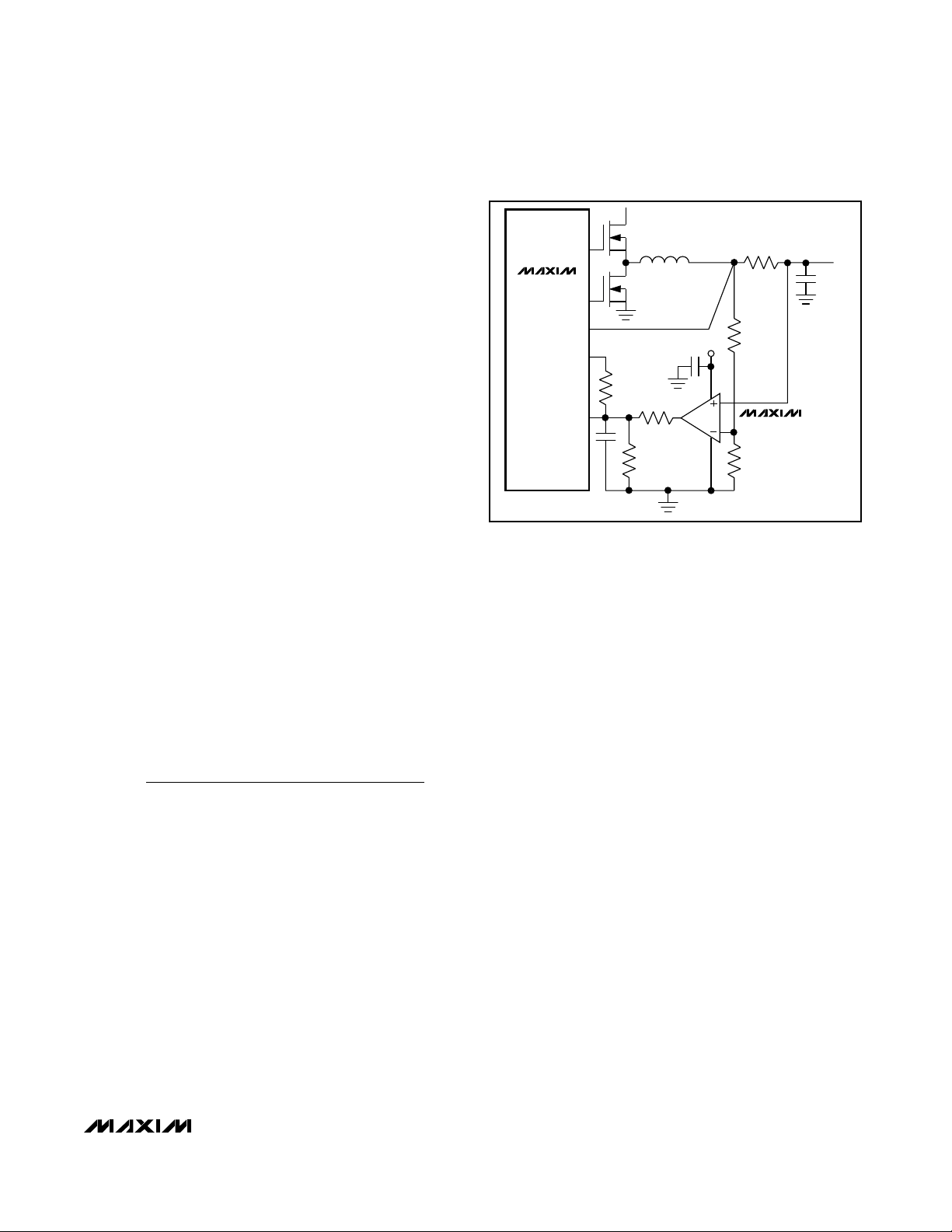
MAX1718
Notebook CPU Step-Down Controller for Intel
Mobile Voltage Positioning (IMVP-II)
______________________________________________________________________________________ 29
iting occurs. The op amp causes current limiting by
lowering the voltage on the ILIM pin. This lowers the
current-limit threshold of the IC’s internal current-limit
circuit, which uses the MOSFET R
DS(ON)
as usual. The
op-amp output swing has the ability to adjust the IC’s
internal valley current limit from a value much higher
than ever needed (given the MOSFET’s R
RD(ON)
) to a
value much lower than required to support a normal
load.
The bandwidth of the ILIM pin is not high, so the speed
of the op amp is not critical. Any op amp or comparator
could be acceptable, as long as its input offset does
not degrade current-limit accuracy excessively, has
input common-mode range to ground and has Rail-toRail®output swing. Because the bandwidth is low, the
circuit responds to the average inductor current rather
than the peak or valley current, eliminating the current
limit’s dependence on inductor ripple current.
Similar to a foldback current limit, this circuit must be
carefully designed to guarantee startup. The op amp
must be incapable of setting the current limit to zero or
else the power supply may be unable to start. The
three-way divider from REF to ground to the op-amp
output allows the op amp to vary the MAX1718’s internal current-limit threshold from 21mV (severely limiting
current) to 182mV (more than guaranteeing the maximum required output current). These divider resistors
should be chosen with the required current and the
synchronous rectifier’s R
RD(ON)
in mind to ensure that
the op-amp adjustment range is high enough to guarantee the required output current. The voltage at the
ILIM pin is given by:
where V
COMP
is the voltage at the output of the com-
parator. The minimum V
ILIM
is calculated when V
COMP
is at the VOLof the comparator. The maximum V
ILIM
is
calculated when V
COMP
= VOHat the minimum VCC.
The valley current-limit threshold is set at 10% of the
voltage V
ILIM
. C13 should be picked to give approxi-
mately 10µs time constant at the ILIM input.
The actual threshold at which the op amp begins to
limit current is determined by R8 and the R10/R11
divider values and is very easy to set. Ideally,
I
OUT(MAX)
✕
R8 = V
FB
✕
R10 / (R10 + R11). In practice,
some margin must be added for resistor accuracy, opamp input offset, and general safety. With the op amp
shown and ±1% resistors, 10% margin is adequate.
An additional benefit of this circuit is that the currentlimit value is proportional to the output voltage setting
(V
FB
). When the output voltage setting is lowered, the
current limit automatically adjusts to a more appropriate
level, providing additional protection without compromising performance since the reduction of the required
load current is greater than that of the output voltage
setting. In some cases, the current required to slew the
output capacitor may be large enough to require the
current limit to be increased beyond what is necessary
to support the load.
This circuit is completely compatible with the circuit of
Figure 15. If the two circuits are used together, the
MAX4326 dual op amp in a µMAX package can
replace the two single devices, saving space and cost.
If both are used, the reduced R8 value makes the opamp input offset more significant. Additional margin
might be needed, depending on the magnitude of R8’s
reduction.
Although the op amp should be placed near R8 to minimize input noise pickup, power it from the MAX1718’s
quiet VCCsupply and analog ground to prevent other
noise problems.
Using Skip Mode During Suspend
(SKP/
SDN
= VCC)
Typically, for the MAX1718’s intended application, the
minimum output currents are too high to benefit from
pulse-skipping operation in all active CPU modes.
Furthermore, Skip mode can be a hindrance to properly
executing downward output voltage transitions (see the
V
RRV RRV
RR RR R R
ILIM
REF COMP
=
×× + ××
[]
×+×+×
[]
()( )
()()( )
12 13 13 14
12 14 12 13 13 14
Rail-to-Rail is a registered trademark of Nippon Motorola, Ltd.
DL
DH
R10
1.5kΩ
1nF
MAX1718
R8
4mΩ
V
CC
V
OUT
1.25V, 19A
ILIM
REF
FB
MAX4322
R14
100kΩ
R13
20kΩ
R11
20kΩ
R12
30kΩ
Figure 16. Improving Current-Limit Accuracy

MAX1718
Notebook CPU Step-Down Controller for Intel
Mobile Voltage Positioning (IMVP-II)
30 ______________________________________________________________________________________
Forced-PWM Mode section). However, processor suspend currents can be low enough that Skip mode operation provides a real benefit.
In the circuit of Figure 17, SKP/SDN remains biased at
2V in every state except Suspend and Shutdown. In
addition, upon entering Suspend (SUS going high) the
pin remains at 2V for about 200µs before it eventually
goes high. This causes the MAX1718 to remain in PWM
mode long enough to correctly complete the negative
output voltage transition to the Suspend state voltage.
When SKP/SDN goes high, the MAX1718 enters its lowquiescent-current Skip mode.
Dropout Performance
The output voltage adjust range for continuous-conduction operation is restricted by the nonadjustable 500ns
(max) minimum off-time one-shot (375ns max at
1000kHz). For best dropout performance, use the slower
(200kHz) on-time settings. When working with low input
voltages, the duty-factor limit must be calculated using
worst-case values for on- and off-times. Manufacturing
tolerances and internal propagation delays introduce
an error to the TON K-factor. This error is greater at
higher frequencies (Table 2). Also, keep in mind that
transient response performance of buck regulators
operated close to dropout is poor, and bulk output
capacitance must often be added (see the VSAG equation in the Design Procedure section).
The absolute point of dropout is when the inductor current ramps down during the minimum off-time (∆I
DOWN
)
as much as it ramps up during the on-time (∆I
UP
). The
ratio h = ∆I
UP
/∆I
DOWN
is an indicator of ability to slew
the inductor current higher in response to increased
load, and must always be greater than 1. As h
approaches 1, the absolute minimum dropout point, the
inductor current will be less able to increase during
each switching cycle and V
SAG
will greatly increase
unless additional output capacitance is used.
A reasonable minimum value for h is 1.5, but this may
be adjusted up or down to allow tradeoffs between
V
SAG
, output capacitance, and minimum operating
voltage. For a given value of h, the minimum operating
voltage can be calculated as:
where V
DROP1
and V
DROP2
are the parasitic voltage
drops in the discharge and charge paths, respectively
(see the On-Time One-Shot (TON) section), T
OFF(MIN)
is
from the Electrical Characteristics tables, and K is taken
from Table 2. The absolute minimum input voltage is calculated with h = 1.
If the calculated V
IN(MIN)
is greater than the required
minimum input voltage, then operating frequency must
be reduced or output capacitance added to obtain an
acceptable V
SAG
. If operation near dropout is anticipat-
ed, calculate V
SAG
to be sure of adequate transient
response.
Dropout Design Example:
V
OUT
= 1.6V
fsw = 550kHz
K = 1.8µs, worst-case K = 1.58µs
T
OFF(MIN)
= 500ns
V
DROP1
= V
DROP2
= 100mV
h = 1.5
V
IN(MIN)
= (1.6V + 0.1V) / (1-0.5µs x 1.5/1.58µs) + 0.1V
- 0.1V = 3.2V
Calculating again with h = 1 gives the absolute limit of
dropout:
V
IN(MIN)
= (1.6V + 0.1V) / (1-1.0 ✕0.5µs/1.58µs) - 0.1V
+ 0.1V = 2.5V
Therefore, VINmust be greater than 2.5V, even with very
large output capacitance, and a practical input voltage
with reasonable output capacitance would be 3.2V.
Adjusting V
OUT
with a Resistor-Divider
The output voltage can be adjusted with a resistordivider rather than the DAC if desired (Figure 18). The
drawback is that the on-time doesn’t automatically
receive correct compensation for changing output voltage
levels. This can result in variable switching frequency
as the resistor ratio is changed, and/or excessive
switching frequency. The equation for adjusting the output
voltage is:
where VFBis the currently selected DAC value. In resistor-adjusted circuits, the DAC code should be set as
close as possible to the actual output voltage in order
to minimize the shift in switching frequency.
One-Stage (Battery Input) vs. Two-Stage
(5V Input) Applications
The MAX1718 can be used with a direct battery connection (one stage) or can obtain power from a regulated 5V
supply (two stage). Each approach has advantages,
VV
R
R
OUT FB
=+
1
1
2
V
VV
T
xh
K
VV
IN MIN
OUT DROP
OFF MIN
DROP DROP()
()
=
+
()
−
+−
1
21
1

MAX1718
Notebook CPU Step-Down Controller for Intel
Mobile Voltage Positioning (IMVP-II)
______________________________________________________________________________________ 31
and careful consideration should go into the selection of
the final design.
The one-stage approach offers smaller total inductor
size and fewer capacitors overall due to the reduced
demands on the 5V supply. The transient response of
the single stage is better due to the ability to ramp up
the inductor current faster. The total efficiency of a single stage is better than the two-stage approach.
The two-stage approach allows flexible placement due
to smaller circuit size and reduced local power dissipation. The power supply can be placed closer to the
CPU for better regulation and lower I
2
R losses from PC
board traces. Although the two-stage design has worse
transient response than the single stage, this can be
offset by the use of a voltage-positioned converter.
Ceramic Output Capacitor
Applications
Ceramic capacitors have advantages and disadvantages. They have ultra-low ESR and are noncombustible, relatively small, and nonpolarized. They are
also expensive and brittle, and their ultra-low ESR characteristic can result in excessively high ESR zero frequencies (affecting stability in nonvoltage-positioned
circuits). In addition, their relatively low capacitance
value can cause output overshoot when going abruptly
from full-load to no-load conditions, unless the inductor
value can be made small (high switching frequency), or
there are some bulk tantalum or electrolytic capacitors
in parallel to absorb the stored energy in the inductor.
In some cases, there may be no room for electrolytics,
creating a need for a DC-DC design that uses nothing
but ceramics.
The MAX1718 can take full advantage of the small size
and low ESR of ceramic output capacitors in a voltagepositioned circuit. The addition of the positioning resistor
increases the ripple at FB, lowering the effective ESR
zero frequency of the ceramic output capacitor.
Output overshoot (V
SOAR
) determines the minimum
output capacitance requirement (see the Output
Capacitor Selection section). Often the switching frequency is increased to 550kHz or 1000kHz, and the inductor
value is reduced to minimize the energy transferred from
inductor to capacitor during load-step recovery. The efficiency penalty for operating at 550kHz is about 2% to 3%
and about 5% at 1000kHz when compared to the
300kHz voltage-positioned circuit, primarily due to the
high-side MOSFET switching losses.
PC Board Layout Guidelines
Careful PC board layout is critical to achieve low
switching losses and clean, stable operation. The
switching power stage requires particular attention
(Figure 19). If possible, mount all of the power components on the top side of the board with their ground terminals flush against one another. Follow these
guidelines for good PC board layout:
1) Keep the high-current paths short, especially at the
ground terminals. This is essential for stable, jitterfree operation.
2) All analog grounding is done to a separate solid cop-
per plane, which connects to the MAX1718 at the
GND pin. This includes the VCC, REF, and CC
30kΩ
3.3V
5V
SHUTDOWN
TO
SKP/SDN
SUS
SKP/SDN
~200µs~200µs
0V
2.0V
TO
SUS
V
CC
0.01µF
V
CC
120kΩ
80kΩ
Figure 17. Using Skip Mode During Suspend (SKP/ SDN = VCC)
DL
DH
FB
V
BATT
V
OUT
R1
R2
MAX1718
V
OUT
= VFB x
(
1 + )
R1
R2
Figure 18. Adjusting V
OUT
with a Resistor-Divider

MAX1718
Notebook CPU Step-Down Controller for Intel
Mobile Voltage Positioning (IMVP-II)
32 ______________________________________________________________________________________
capacitors, the TIME resistor, as well as any other
resistor-dividers.
3) Keep the power traces and load connections short.
This is essential for high efficiency. The use of thick
copper PC boards (2oz vs. 1oz) can enhance fullload efficiency by 1% or more. Correctly routing PC
board traces is a difficult task that must be
approached in terms of fractions of centimeters,
where a single milliohm of excess trace resistance
causes a measurable efficiency penalty.
4) LX and GND connections to Q2 for current limiting
must be made using Kelvin sense connections to
guarantee the current-limit accuracy. With SO-8
MOSFETs, this is best done by routing power to the
MOSFETs from outside using the top copper layer,
while connecting GND and LX inside (underneath)
the SO-8 package.
5) When trade-offs in trace lengths must be made, it’s
preferable to allow the inductor charging path to be
made longer than the discharge path. For example,
it’s better to allow some extra distance between the
input capacitors and the high-side MOSFET than to
allow distance between the inductor and the low-side
MOSFET or between the inductor and the output filter
capacitor.
6) Ensure the FB connection to the output is short and
direct. In voltage-positioned circuits, the FB connection
is at the junction of the inductor and the positioning
resistor.
7) Route high-speed switching nodes away from sensitive
analog areas (CC, REF, ILIM). Make all pin-strap
control input connections (SKP/SDN, ILIM, etc.) to analog ground or VCCrather than power ground or VDD.
Layout Procedure
1) Place the power components first, with ground terminals adjacent (Q2 source, CIN-, COUT-, D1 anode).
If possible, make all these connections on the top
layer with wide, copper-filled areas.
2) Mount the controller IC adjacent to MOSFET Q2,
preferably on the back side opposite Q2 in order to
keep LX-GND current-sense lines and the DL drive line
short and wide. The DL gate trace must be short and
wide, measuring 10 to 20 squares (50mils to 100mils
wide if the MOSFET is 1 inch from the controller IC).
3) Group the gate-drive components (BST diode and
capacitor, V
DD
bypass capacitor) together near the
controller IC.
4) Make the DC-DC controller ground connections as
shown in Figure 19. This diagram can be viewed as
having three separate ground planes: output ground,
where all the high-power components go; the GND
plane, where the GND pin and VDDbypass capacitors
go; and an analog ground plane where sensitive
analog components go. The analog ground plane
and GND plane must meet only at a single point
directly beneath the IC. These two planes are then
connected to the high-power output ground with a
short connection from GND to the source of the lowside MOSFET Q2 (the middle of the star ground).
This point must also be very close to the output
capacitor ground terminal.
5) Connect the output power planes (VCORE and system
ground planes) directly to the output filter capacitor
positive and negative terminals with multiple vias.
Place the entire DC-DC converter circuit as close to
the CPU as is practical.
Chip Information
TRANSISTOR COUNT: 7190

MAX1718
Notebook CPU Step-Down Controller for Intel
Mobile Voltage Positioning (IMVP-II)
______________________________________________________________________________________ 33
D1 Q2
V
BATT
GND IN
COUT
VIA TO FB
AND FBS
VIA TO LX
VIA TO SOURCE
OF Q2
VIA TO GND
NEAR Q2 SOURCE
INDUCTOR DISCHARGE PATH HAS LOW DC RESISTANCE
GND
OUT
V
OUT
L1
Q1
CC
V
CC
V
DD
REF
ALL ANALOG GROUNDS
CONNECT TO LOCAL PLANE ONLY
NOTES: "STAR" GROUND IS USED.
D1 IS DIRECTLY ACROSS Q2.
CONNECT LOCAL ANALOG GROUND PLANE DIRECTLY TO GND FROM
THE SIDE OPPOSITE THE V
DD
CAPACITOR GND TO AVOID VDD GROUND
CURRENTS FROM FLOWING IN THE ANALOG GROUND PLANE.
MAX1718
CIN
R6
GND
Figure 19. Power-Stage PC Board Layout Example

MAX1718
Notebook CPU Step-Down Controller for Intel
Mobile Voltage Positioning (IMVP-II)
34 ______________________________________________________________________________________
28
27
26
25
24
23
22
21
20
19
18
17
16
15
1
2
3
4
5
6
7
8
9
10
11
12
13
14
DH
LX
BST
D0
D1
D2
GND
D3
D4
OVP
ZMODE
SUS
V
DD
DL
VGATE
POS
ILIM
REF
TON
V
CC
S1
S0
CC
NEG
FB
TIME
SKP/SDN
V+
QSOP
TOP VIEW
MAX1718
Pin Configuration

Maxim cannot assume responsibility for use of any circuitry other than circuitry entirely embodied in a Maxim product. No circuit patent licenses are
implied. Maxim reserves the right to change the circuitry and specifications without notice at any time.
35 ____________________Maxim Integrated Products, 120 San Gabriel Drive, Sunnyvale, CA 94086 408-737-7600
© 2005 Maxim Integrated Products Printed USA is a registered trademark of Maxim Integrated Products, Inc.
QSOP.EPS
Note: The MAX1718 does not have a heat slug.
Notebook CPU Step-Down Controller for Intel
Mobile Voltage Positioning (IMVP-II)
MAX1718
Package Information
(The package drawing(s) in this data sheet may not reflect the most current specifications. For the latest package outline information,
go to www.maxim-ic.com/packages.)

 Loading...