

Page 1
For price, delivery, and to place orders, please contact Maxim Distribution at 1-888-629-4642,
or visit Maxim’s website at www.maxim-ic.com.
General Description
The MAX1715 PWM controller provides the high efficiency, excellent transient response, and high DC output accuracy needed for stepping down high-voltage
batteries to generate low-voltage CPU core, I/O, and
chipset RAM supplies in notebook computers.
Maxim’s proprietary Quick-PWM™ quick-response,
constant-on-time PWM control scheme handles wide
input/output voltage ratios with ease and provides
100ns “instant-on” response to load transients while
maintaining a relatively constant switching frequency.
The MAX1715 achieves high efficiency at a reduced
cost by eliminating the current-sense resistor found in
traditional current-mode PWMs. Efficiency is further
enhanced by its ability to drive very large synchronousrectifier MOSFETs.
Single-stage buck conversion allows this device to
directly step down high-voltage batteries for the highest
possible efficiency. Alternatively, two-stage conversion
(stepping down the +5V system supply instead of the
battery) at a higher switching frequency allows the minimum possible physical size.
The MAX1715 is intended for CPU core, chipset,
DRAM, or other low-voltage supplies as low as 1V. The
MAX1715 is available in a 28-pin QSOP package. For
applications requiring VID compliance or DAC control
of output voltage, refer to the MAX1710/MAX1711 data
sheet. For a single-output version, refer to the MAX1714
data sheet.
Applications
Notebook Computers
CPU Core Supply
Chipset/RAM Supply as Low as 1V
1.8V and 2.5V I/O Supply
Features
♦ Ultra-High Efficiency
♦ No Current-Sense Resistor (lossless I
LIMIT
)
♦ Quick-PWM with 100ns Load-Step Response
♦ 1% V
OUT
Accuracy over Line and Load
♦ Dual-Mode Fixed 1.8V/3.3V/Adj or 2.5V/Adj Outputs
♦ Adjustable 1V to 5.5V Output Range
♦ 2V to 28V Battery Input Range
♦ 200/300/420/540kHz Nominal Switching Frequency
♦ Over/Undervoltage Protection
♦ 1.7ms Digital Soft-Start
♦ Drives Large Synchronous-Rectifier FETs
♦ Power-Good Indicator
MAX1715
Ultra-High Efficiency, Dual Step-Down
Controller for Notebook Computers
________________________________________________________________ Maxim Integrated Products 1
19-1541; Rev 2; 8/05
Pin Configuration appears at end of data sheet.
Quick-PWM is a trademark of Maxim Integrated Products.
Ordering Information
EVALUATION KIT
AVAILABLE
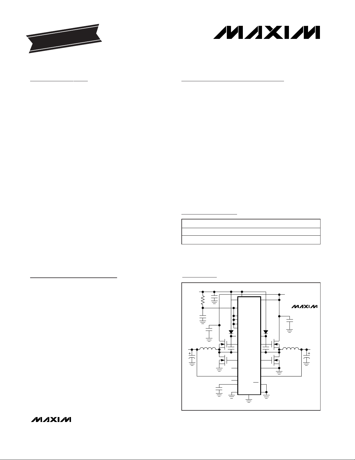
V
CC
OUTPUT1
1.8V
BATTERY
4.5V TO 28V
ILIM1
ON2
DL1
TON
OUT1
LX1
DH1
FB1 AGND
V
DD
BST1
ILIM2
ON1
REF
DL2
PGND
OUT2
LX2
DH2
FB2
V+
BST2
SKIP
5V INPUT
PGOOD
OUTPUT2
2.5V
MAX1715
Minimal Operating Circuit
PART TEMP RANGE PIN-PACKAGE
MAX1715EEI -40°C to +85°C 28 QSOP
MAX1715EEI+
-40°C to +85°C 28 QSOP
+ Denotes lead-free package.
Page 2
MAX1715
Ultra-High Efficiency, Dual Step-Down
Controller for Notebook Computers
2 _______________________________________________________________________________________
ABSOLUTE MAXIMUM RATINGS
Stresses beyond those listed under “Absolute Maximum Ratings” may cause permanent damage to the device. These are stress ratings only, and functional
operation of the device at these or any other conditions beyond those indicated in the operational sections of the specifications is not implied. Exposure to
absolute maximum rating conditions for extended periods may affect device reliability.
V+ to AGND..............................................................-0.3 to +30V
V
DD
, VCCto AGND..................................................-0.3V to +6V
PGND to AGND or V
CC
to VDD...........................................±0.3V
PGOOD, OUT_ to AGND..........................................-0.3V to +6V
ILIM_, FB_, REF,
SKIP, TON,
ON_ to AGND...........................................-0.3V to (V
DD
+ 0.3V)
DL_ to PGND..............................................-0.3V to (V
DD
+ 0.3V)
BST_ to AGND........................................................-0.3V to +36V
DH1 to LX1 ...............................................-0.3V to (BST1 + 0.3V)
DH2 to LX2 ...............................................-0.3V to (BST2 + 0.3V)
LX1 to BST1..............................................................-6V to +0.3V
LX2 to BST2..............................................................-6V to +0.3V
REF Short Circuit to AGND.........................................Continuous
Continuous Power Dissipation (T
A
= +70°C)
28-Pin QSOP (derate 8.0mW/°C above +70°C).....640mW/°C
Operating Temperature Range ..........................-40°C to +85°C
Junction Temperature......................................................+150°C
Storage Temperature Range ............................-65°C to +150°C
Lead Temperature (soldering, 10s) .................................+300°C
ELECTRICAL CHARACTERISTICS
(Circuit of Figure 1, 4A components from Table 1, V
CC = VDD
= +5V, SKIP = AGND, V+ = 15V, TA= 0°C to +85°C, unless otherwise
noted.) (Note 1)
I
LOAD
= 0 to 4A, each output %0.4
FB2 = GND
Battery voltage, V+
Input Voltage Range
V+ = 24V, OUT2 = 2V
Load Regulation Error
VCC= 4.5V to 5.5V, V+ = 4.5V to 28V
V+ = 24V, OUT1 = 2V
Adjustable mode, each output
Output 2 Error Comparator
Threshold (DC Output Voltage
Accuracy) (Note 2)
TON = GND
FB_ Input Bias Current
TON = GND
TON = open
V
OUT
_ = AGND
210 247 280
CONDITIONS
V
TON = REF
142 173 205
ms
TON = V
DD
OUT_ Input Resistance
µA
Soft-Start Ramp Time
ΩFB_ = AGND
Rising edge of ON_ to full current limit
2.475 2.5 2.525
V+ = 2V to 28V,
SKIP = V
CC
, TA = +25°C
I
LOAD
= 0 to 4A
V+ = 2V to 28V,
SKIP = V
CC
, TA = +25°C
I
LOAD
= 0 to 4A
ns
154 182 215
V
On-Time (PWM2)
ns
112 136 160
0.99 1.00 1.01
On-Time (PWM1)
V
1.7
0.99 1.00 1.01
300 353 407
1.782 1.8 1.818
-0.1 0.1
TON = open
292 336 380
TON = REF
75k
3.267 3.3 3.333
FB1 = V
CC
FB1 = AGND
FB1 = OUT1
228
FB2 = OUT2
V
1 5.5
Output Voltage Range
%0.2
198 234 270
Line Regulation Error
TON = V
DD
420 484 550
UNITSMIN TYP MAXPARAMETER
Output 1 Error Comparator
Threshold (DC Output Voltage
Accuracy) (Note 2)
4.5 5.5
V
DD,VCC
Output 1 Error Comparator
Threshold (DC Output Voltage
Accuracy) (Note 2)
V+ = 2V to 28V,
SKIP = V
CC
, TA = 0°C to +85°C
I
LOAD
= 0 to 4A
V
0.985 1.00 1.105
1.773 1.8 1.827
3.250 3.3 3.350
FB1 = V
CC
FB1 = AGND
FB1 = OUT1
FB2 = GND
Output 2 Error Comparator
Threshold (DC Output Voltage
Accuracy) (Note 2)
2.463 2.5 2.538
V+ = 2V to 28V,
SKIP = V
CC
, TA = 0°C to +85°C
I
LOAD
= 0 to 4A
V
0.985 1.00 1.105
FB2 = OUT2
Page 3

MAX1715
Ultra-High Efficiency, Dual Step-Down
Controller for Notebook Computers
_______________________________________________________________________________________ 3
ELECTRICAL CHARACTERISTICS (continued)
(Circuit of Figure 1, 4A components from Table 1, V
CC = VDD
= +5V, SKIP = AGND, V+ = 15V, TA= 0°C to +85°C, unless otherwise
noted.) (Note 1)
(Note 3) ns400 500Minimum Off-Time
I
REF
= 0 to 50µA
No external REF load
ON1 = ON2 = 0
V2 0.01Reference Load Regulation
V1.98 2 2.02Reference Voltage
µA<1 5Shutdown Supply Current (V+)
µA<1 5
Shutdown Supply Current
(VCC+ VDD)
Falling edge, hysteresis = 40mV V1.6REF Fault Lockout Voltage
10
PGND - LX_, I
LIM
resistor = 100kΩ
mV
40 50 60
Current-Limit Threshold
(Positive Direction, Adjusted)
PGND - LX_, TA= +25°C, I
LIM
= V
CC
mV-145 -120 -95
Current-Limit Threshold
(Negative Direction)
PGND - LX_, SKIP = AGND
mV-5 3 10
Current-Limit Threshold, Zero
Crossing
Hysteresis = 10°C °C150Thermal Shutdown Threshold
Rising edge, hysteresis = 20mV, PWM disabled below
this level
V4.1 4.4
VCCUndervoltage Lockout
Threshold
BST - LX forced to 5V Ω1.5 5DH Gate Driver On-Resistance
FB1 and FB2 forced above the regulation point µA1100 1600
Quiescent Supply Current
(VCC+ VDD)
µA25 70Quiescent Battery Current (V+)
FB_ forced 2% above trip threshold µs1.5
Overvoltage Fault Propagation
Delay
With respect to error comparator threshold %8.5 10.5 13Overvoltage Trip Threshold
With respect to error comparator threshold %60 70 80Output Undervoltage Threshold
From ON_ signal going high ms10 20 30
Output Undervoltage Lockout
Time
PGND - LX_, I
LIM
= V
CC
mV75 100 125
Current-Limit Threshold
(Positive Direction, Fixed)
ON1 = ON2 = 0
DL, high state Ω1.5 5
DL Gate Driver On-Resistance
(pull-up)
0.6 2.5
A
DH Gate Driver Source/Sink
Current
DH forced to 2.5V, BST_ - LX_ forced to 5V 1
ADL Gate Driver Source Current DL forced to 2.5V 1
ADL Gate Driver Sink Current DL forced to 2.5V 3
nsDead Time
DL rising 35
REF in regulationREF Sink Current
DL, low state
DL Gate Driver On-Resistance
(pull-down)
Ω
µA
CONDITIONS UNITSMIN TYP MAXPARAMETER
PGND - LX_, I
LIM
resistor = 400kΩ 160 200 240
DH rising 26
ON_, SKIP
0.8
VLogic Input High Voltage
ON_, SKIP
2.4
VLogic Input Low Voltage
Page 4
MAX1715
Ultra-High Efficiency, Dual Step-Down
Controller for Notebook Computers
4 _______________________________________________________________________________________
ELECTRICAL CHARACTERISTICS
(Circuit of Figure 1, 4A components from Table 1, V
CC = VDD
= +5V, SKIP = AGND, V+ = 15V, TA= -40°C to +85°C, unless otherwise
noted.) (Note 1)
ELECTRICAL CHARACTERISTICS (continued)
(Circuit of Figure 1, 4A components from Table 1, V
CC = VDD
= +5V, SKIP = AGND, V+ = 15V, TA= 0°C to +85°C, unless otherwise
noted.) (Note 1)
CONDITIONS
V
CC
level
V
VCC- 0.4
TON Threshold
Float level 3.15 3.85
REF level 1.65 2.35
AGND level 0.5
TON (0 or VCC) µA-3 3Logic Input Current
UNITSMIN TYP MAXPARAMETER
On-Time (PWM1)
112 136 160
ns
FB2 = GND
FB2 = OUT2
V+ = 4.5V to 28V,
SKIP = V
CC
3.234 3.3 3.372FB1 = V
CC
FB1 = AGND
FB1 = OUT1
1.764 1.8 1.836
Minimum Off-Time 400 500 ns(Note 3)
2.45 2.5 2.55
Output 2 Error Comparator
Threshold (DC Output Voltage
Accuracy) (Note 2)
0.98 1.00 1.02
V
PARAMETER MIN TYP MAX UNITS
Input Voltage Range
228
V
4.5 5.5
Output 1 Error Comparator
Threshold (DC Output Voltage
Accuracy) (Note 2)
0.98 1.00 1.02
V
CONDITIONS
Battery voltage, V+
V
DD, VCC
V+ = 2V to 28V,
SKIP = V
CC
On-Time (PWM2)
154 182 215
ns
ON_, SKIP (0 or VCC)
µA-1 1Logic Input Current
Falling edge, FB_ forced 2% below PGOOD trip threshold µs1.5PGOOD Propagation Delay
Measured at FB_, with respect to error comparator
threshold, no load
%-8 -5.5 -4PGOOD Trip Threshold
I
SINK
= 1mA V0.1 0.4PGOOD Output Low Voltage
High state, forced to 5.5V µA1PGOOD Leakage Current
SKIP, to deactivate OVP circuitry
mA-5 -1Logic Input Current
210 247 280
142 173 205
300 353 407
292 336 380
198 234 270
V+ = 24V, OUT2 = 2V
420 484 550
TON = GND
TON = REF
TON = open
TON = V
DD
V+ = 24V, OUT1 = 2V
TON = GND
TON = REF
TON = open
TON = V
DD
Page 5
MAX1715
Ultra-High Efficiency, Dual Step-Down
Controller for Notebook Computers
_______________________________________________________________________________________ 5
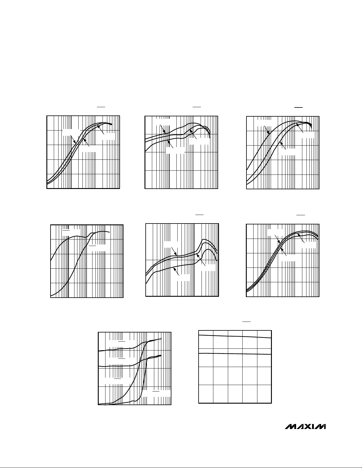
60
0.01 1010.1
90
100
80
70
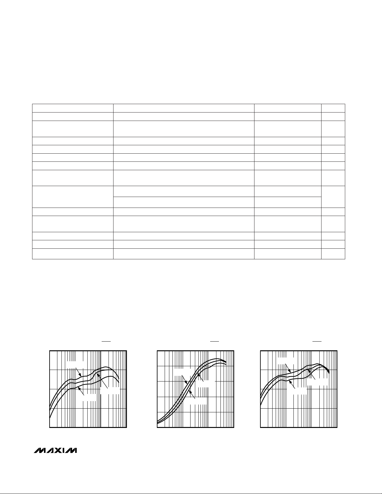
MAX1715-01
LOAD CURRENT (A)
EFFICIENCY (%)
EFFICIENCY vs. LOAD CURRENT
(1.8V, 4A COMPONENTS, SKIP = GND)
V+ = +7V
V+ = +12V
V+ = +20V
0
0.01 1010.1
60
80
100
40
20
MAX1715-02
LOAD CURRENT (A)
EFFICIENCY (%)
EFFICIENCY vs. LOAD CURRENT
(1.8V, 4A COMPONENTS, SKIP = V
CC
)
V+ = +7V
V+ = +20V
V+ = +12V
60
0.01 1010.1
90
100
80
70
MAX1715-03
LOAD CURRENT (A)
EFFICIENCY (%)
EFFICIENCY vs. LOAD CURRENT
(2.5V, 4A COMPONENTS, SKIP = GND)
V+ = +7V
V+ = +20V
V+ = +12V
Note 1: Specifications to -40°C are guaranteed by design, and not production tested.
Note 2: When the inductor is in continuous conduction, the output voltage will have a DC regulation higher than the trip level by
50% of the ripple. In discontinuous conduction (SKIP = AGND, light load) the output voltage will have DC regulation
higher than the trip level by approximately 1.5% due to slope compensation.
Note 3: On-time and off-time specifications are measured from the 50% point at the DH pin with LX = PGND, V
BST
= 5V. Actual
in-circuit times may differ due to MOSFET switching speeds.
__________________________________________Typical Operating Characteristics
(Circuit of Figure 1, components from Table 1, VIN= +15V, SKIP = AGND, TON = unconnected, TA= +25°C, unless otherwise noted.)
ELECTRICAL CHARACTERISTICS (continued)
(Circuit of Figure 1, 4A components from Table 1, V
CC = VDD
= +5V, SKIP = AGND, V+ = 15V, TA= -40°C to +85°C, unless otherwise
noted.) (Note 1)
Quiescent Battery Current (V+) 25 70 µA
Reference Voltage 1.97 2 2.03 VNo external REF load
Quiescent Supply Current
(VCC+ VDD)
1100 1600 µAFB1 and FB2 forced above the regulation point
PARAMETER MIN TYP MAX UNITSCONDITIONS
Reference Load Regulation 0.01 VI
REF
= 0 to 50µA
Overvoltage Trip Threshold 10 12.5 15 %With respect to error comparator threshold
Output Undervoltage Threshold 60 70 80 %With respect to error comparator threshold
Current-Limit Threshold (positive
direction, fixed)
75 100 125 mVPGND - LX_, I
LIM
= V
CC
Current-Limit Threshold (positive
direction, adjusted)
32 50 62
mV
PGND - LX_, I
LIM
resistor = 100kΩ
PGND - LX_, I
LIM
resistor = 400kΩ 160 200 240
Thermal Shutdown Threshold 150 °CHysteresis = 10°C
Rising edge, hysteresis = 20mV, PWM disabled below
this level
4.1 4.4 V
VCCUndervoltage Lockout
Threshold
Logic Input High Voltage 2.4 V
ON_, SKIP
ON_, SKIP
0.8 VLogic Input Low Voltage
SKIP, to deactivate OVP circuitry
-5 -1 mALogic Input Current
Page 6
MAX1715
Ultra-High Efficiency, Dual Step-Down
Controller for Notebook Computers
6 _______________________________________________________________________________________
_____________________________Typical Operating Characteristics (continued)
(Circuit of Figure 1, components from Table 1, VIN= +15V, SKIP = AGND, TON = unconnected, TA= +25°C, unless otherwise noted.)
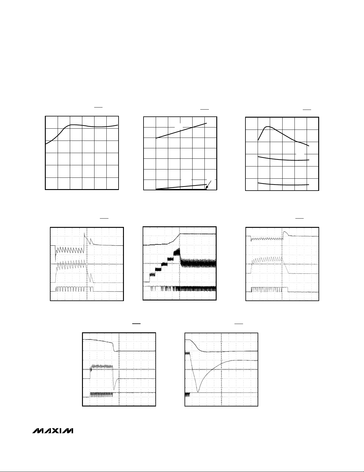
0
0.01 1010.1
60
80
100
40
20
MAX1715-9
LOAD CURRENT (A)
EFFICIENCY (%)
EFFICIENCY vs. LOAD CURRENT
(1.3V, 8A COMPONENTS, SKIP = V
CC
)
V+ = +7V
V+ = +20V
V+ = +12V
0
0.01 1010.1
300
400
200
100
MAX1715-10
LOAD CURRENT (A)
FREQUENCY (kHz)
FREQUENCY vs. LOAD CURRENT
(4A COMPONENTS)
OUT1, SKIP = V
CC
OUT2, SKIP = V
CC
OUT1, SKIP = GND
OUT2, SKIP = GND
400
300
200
100
0
4128 162024
MAX1715-11
SUPPLY VOLTAGE (V)
FREQUENCY (kHz)
FREQUENCY vs. SUPPLY VOLTAGE
(4A COMPONENTS, SKIP = V
CC
)
OUT1
OUT2
100
80
60
40
20
0
0.001 0.1 10.01 10
MAX1715-07
LOAD CURRENT (A)
EFFICIENCY (%)
EFFICIENCY vs. LOAD CURRENT
(3.3V, 1.5A COMPONENTS, V
IN
= 5V)
SKIP = V
CC
SKIP = GND
60
0.01 1010.1
80
100
MAX1715-08
LOAD CURRENT (A)
EFFICIENCY (%)
EFFICIENCY vs. LOAD CURRENT
(1.3V, 8A COMPONENTS, SKIP = GND)
V+ = +7V
V+ = +20V
V+ = +12V
0
0.01 1010.1
60
80
100
40
20
MAX1715-04
LOAD CURRENT (A)
EFFICIENCY (%)
EFFICIENCY vs. LOAD CURRENT
(2.5V, 4A COMPONENTS, SKIP = V
CC
)
V+ = +7V
V+ = +20V
V+ = +12V
60
0.01 1010.1
90
100
80
70
MAX1715-05
LOAD CURRENT (A)
EFFICIENCY (%)
EFFICIENCY vs. LOAD CURRENT
(5V, 3A COMPONENTS, SKIP = GND)
V+ = +7V
V+ = +20V
V+ = +12V
0
0.01 1010.1
60
80
100
40
20
MAX1715-06
LOAD CURRENT (A)
EFFICIENCY (%)
EFFICIENCY vs. LOAD CURRENT
(5V, 3A COMPONENTS, SKIP = V
CC
)
V+ = +7V
V+ = +20V
V+ = +12V
Page 7
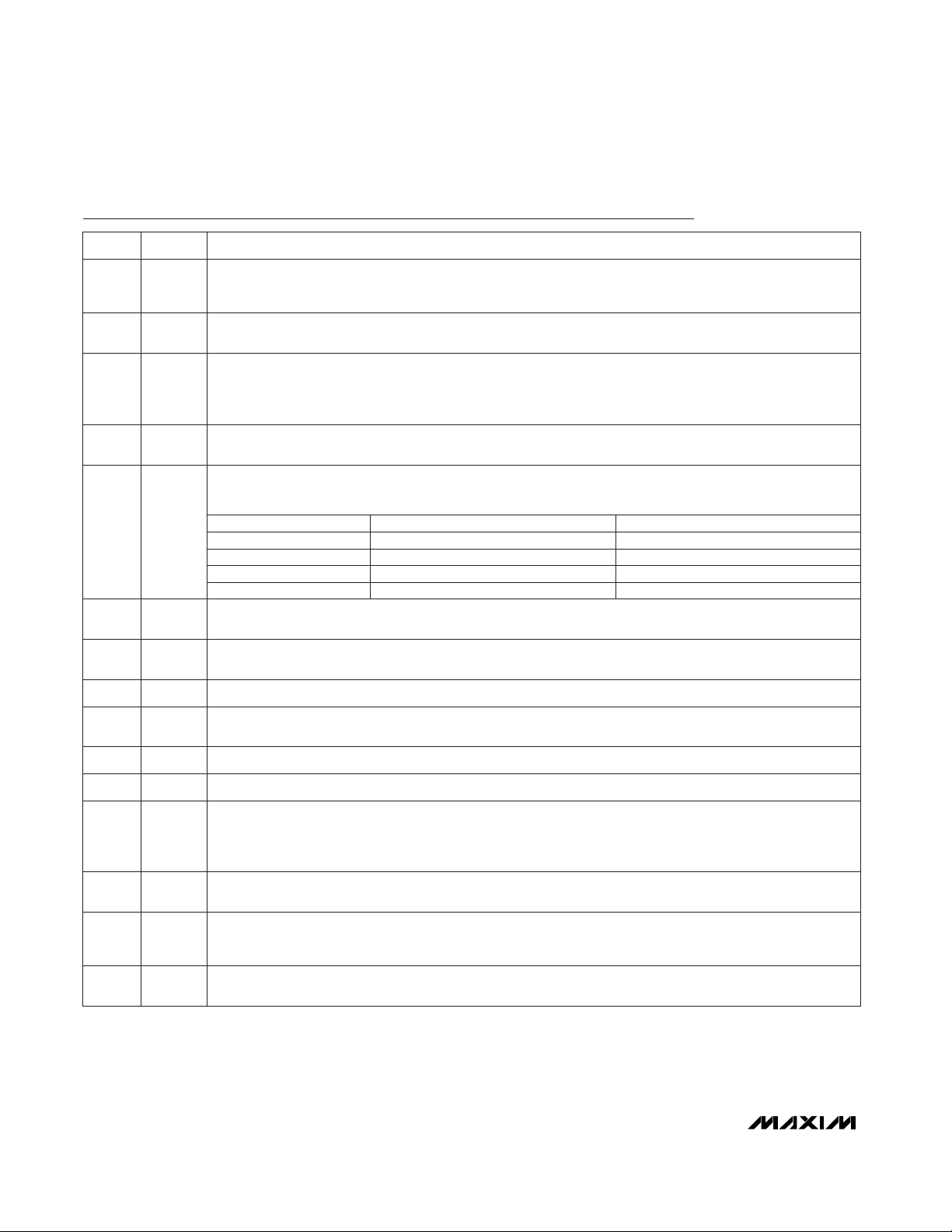
300
200
250
150
100
50
0
-400-20
40
20
60
80
MAX1715-12
TEMPERATURE (°C)
FREQUENCY (kHz)
FREQUENCY vs. TEMPERATURE
(2.5V, 4A COMPONENTS, SKIP = HIGH)
C
A
B
MAX1715-16
A = V
OUT
, 2V/div
B = INDUCTOR CURRENT, 2A/div
C = DL, 10V/div
START-UP WAVEFORM
(2.5V, 4A COMPONENTS, ACTIVE LOAD)
700
500
600
400
300
100
200
0
0105
20
15
25
30
MAX1715-13
INPUT VOLTAGE (V)
SUPPLY CURRENT (μA)
NO-LOAD SUPPLY CURRENT vs. INPUT VOLTAGE
(OUT1 = 1.8V, 4A COMPONENTS;
OUT2 = 2.5V, 4A COMPONENTS; SKIP = GND)
I
DD
I
CC
I
BATT
12
8
10
6
4
2
0
0105
20
15
25
30
MAX1715-14
INPUT VOLTAGE (V)
SUPPLY CURRENT (mA)
NO-LOAD SUPPLY CURRENT vs. INPUT VOLTAGE
(OUT1 = 1.8V, 4A COMPONENTS;
OUT2 = 2.5V, 4A COMPONENTS; SKIP = V
CC
)
I
DD
I
CC
I
IN
C
A
B
MAX1715-17
A = V
OUT
, AC-COUPLED, 100mV/div
B = INDUCTOR CURRENT, 5A/div
C = DL, 10V/div
LOAD-TRANSIENT RESPONSE
(1.3V, 8A COMPONENTS, SKIP = GND)
MAX1715
Ultra-High Efficiency, Dual Step-Down
Controller for Notebook Computers
_______________________________________________________________________________________ 7
_____________________________Typical Operating Characteristics (continued)
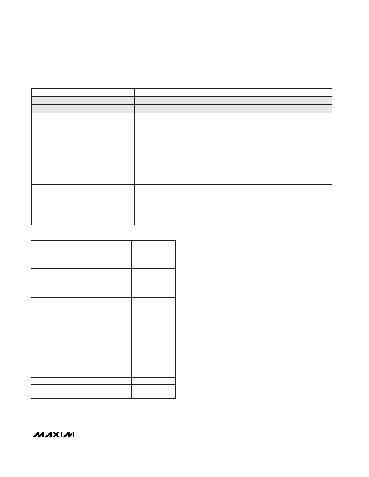
(Circuit of Figure 1, components from Table 1, VIN= +15V, SKIP = AGND, TON = unconnected, TA= +25°C, unless otherwise noted.)
C
A
B
MAX1715-19
A = V
OUT
, 2V/div
B = INDUCTOR CURRENT, 5A/div
C = DL, 10V/div
SHUTDOWN WAVEFORM
(2.5V, 4A COMPONENTS, SKIP = GND)
C
A
B
MAX1715-18
A = V
OUT
, 2V/div
B = INDUCTOR CURRENT, 5A/div
C = DL, 10V/div
OUTPUT OVERLOAD WAVEFORM
(2.5V, 4A COMPONENTS, SKIP = GND)
C
A
B
MAX1715-15
A = V
OUT
, AC-COUPLED, 100mV/div
B = INDUCTOR CURRENT, 2A/div
C = DL, 10V/div
LOAD-TRANSIENT RESPONSE
(2.5V, 4A COMPONENTS, SKIP = GND)
Page 8
170
MAX1715
Ultra-High Efficiency, Dual Step-Down
Controller for Notebook Computers
8 _______________________________________________________________________________________
Pin Description
OUT1 ON/OFF Control Input. Drive to AGND to turn OUT1 off. Drive to VCCto turn OUT1 on.
ON110
Feedback Input for OUT1. Connect to AGND for 1.8V fixed output or to VCCfor 3.3V fixed output, or connect
to a resistor-divider from OUT1 for an adjustable output.
FB12
+2.0V Reference Voltage Connection. Bypass to AGND with 0.22µF (min) capacitor. Can supply 50µA for
external loads.
REF9
Output Voltage Connection for the OUT1 PWM. Connect directly to the junction of the external inductor and
output filter capacitors. OUT1 senses the output voltage to determine the on-time and also serves as the
feedback input in fixed-output modes.
OUT11
Pulse-Skipping Control Input. Connect to VCCfor low-noise forced-PWM mode. Connect to AGND to enable
pulse-skipping operation.
SKIP
6
Power-Good Open-Drain Output. PGOOD is low when either FB_ input is more than 5.5% below the normal
regulation point (typ).
PGOOD7
Analog GroundAGND8
Current-Limit Threshold Adjustment for OUT1. The LX1-PGND current-limit threshold defaults to +100mV if
ILIM1 is connected to VCC. Or, connect an external resistor to AGND to adjust the limit. A precision 5µA pull-up
current through R
EXT
sets the threshold from 50mV to 200mV. The voltage on the pin is 10 times the current-
limit voltage. Choose R
EXT
equal to 2kΩ per mV of current-limit threshold (100kΩ to 400kΩ).
ILIM13
Battery Voltage Sense Connection. Connect to the input power source. V+ is used only to set the PWM oneshot timing.
V+4
PIN
On-Time Selection Control Input. This is a four-level input used to determine DH_ on-time. The TON table
below is for VIN= 24V, V
OUT1
= 1.8V, V
OUT2
= 2.5V condition.
TON5
FUNCTIONNAME
OUT2 ON/OFF Control Input. Drive to AGND to turn OUT2 off. Drive to VCCto turn OUT2 on.
ON211
Current-Limit Threshold Adjustment for OUT2. The LX2-PGND current-limit threshold defaults to +100mV if
ILIM2 is connected to VCC. Or, connect an external resistor to AGND to adjust the limit. A precision 5µA pull-up
current through R
EXT
sets the threshold from 50mV to 200mV. The voltage on the pin is 10 times the current-
limit voltage. Choose R
EXT
equal to 2kΩ per mV of current-limit threshold (100kΩ to 400kΩ).
ILIM212
Feedback Input for OUT2. Connect to AGND for 2.5V fixed output, or connect to a resistor-divider from
OUT2 for an adjustable output.
FB213
Output Voltage Connection for the OUT2 PWM. Connect directly to the junction of the external inductor and
output filter capacitors. OUT2 senses the output voltage to determine the on-time and also serves as the
feedback input in fixed-output mode.
OUT214
No Connection. These pins are not connected to any internal circuitry. Connect the N.C. pins to the ground
plane to enhance thermal conductivity.
N.C.
15, 23,
28
AGND
TON
Open
V
CC
REF
235
345
485
620
Frequency (OUT1) (kHz) Frequency (OUT2) (kHz)
460
355
255
170
Page 9

MAX1715
Ultra-High Efficiency, Dual Step-Down
Controller for Notebook Computers
_______________________________________________________________________________________ 9
Pin Description (continued)
High-Side Gate Driver Output for OUT1. Swings from LX1 to BST1.DH126
High-Side Gate Driver Output for OUT2. Swings from LX2 to BST2.DH217
Boost Flying Capacitor Connection for OUT1. Connect to an external capacitor and diode according to the
Standard Application Circuit (Figure 1). See MOSFET Gate Drivers (DH_, DL_) section.
BST125
External Inductor Connection for OUT2. Connect to the switched side of the inductor. LX2 serves as the
lower supply voltage rail for the DH2 high-side gate driver and is the positive input to the OUT2 current-limit
comparator.
LX216
Analog-Supply Input. Connect to the system supply voltage, +4.5V to +5.5V, with a 20Ω series resistor.
Bypass to AGND with a 1µF ceramic capacitor.
V
CC
21
Power Ground. Connect directly to the low-side MOSFETs’ sources. Serves as the negative input of the current-sense amplifiers.
PGND22
Low-Side Gate Driver Output for OUT1. DL1 swings PGND to VDD.DL124
Boost Flying Capacitor Connection for OUT2. Connect to an external capacitor and diode according to the
Standard Application Circuit (Figure 1). See MOSFET Gate Drivers (DH_, DL_) section.
BST218
Low-Side Gate-Driver Output for OUT2. DL2 swings from PGND to VDD.DL219
PIN
Supply Input for the DL Gate Drivers. Connect to the system supply voltage, +4.5V to +5.5V. Bypass to
PGND with a minimum 4.7µF ceramic capacitor.
V
DD
20
FUNCTIONNAME
External Inductor Connection for OUT1. Connect to the switched side of the inductor. LX1 serves as the
lower supply voltage rail for the DH1 high-side gate driver.
LX127
Page 10

MAX1715
Ultra-High Efficiency, Dual Step-Down
Controller for Notebook Computers
10 ______________________________________________________________________________________
VDD = 5V
BIAS SUPPLY
PINS 15, 23, 28 = N.C.
POWER-GOOD
INDICATOR
MAX1715
V
CC
OUTPUT1
1.8V
V
IN
4.5V TO 28V
D3
CMPSH-3A
ILIM1
ON1
DL1
TON
OUT1
AGND
C3 C4
D1
N2
N4
N3
N1
LX1
DH1
C5
0.1μF
C6
0.1μF
C7
0.22μF
FB1
V
DD
C8
1μF
C1
20
21
25
26
27
24
5
1
9
2
8
10
11
18
17
16
19
22
14
6
13
7
C2
C11
1μF
L1
12
3
L2
BST1
ILIM2
REF
ON1
ON2
DL2
PGND
+5V
100k
OUT2
LX2
DH2
FB2
PGOOD
V+
4
BST2
SKIP
C9
4.7μF
R1
20Ω
OUTPUT2
2.5V
D2
ON/OFF
CONTROLS
Figure 1. Standard Application Circuit
Standard Application Circuit
The standard application circuit (Figure 1) generates
two low-voltage rails for general-purpose use in notebook computers (I/O supply, fixed CPU core supply,
DRAM supply). This DC-DC converter steps down a
battery or AC adapter voltage to voltages from 1.0V to
5.5V with high efficiency and accuracy.
See Table 1 for a list of components for common applications. Table 2 lists component manufacturers.
Detailed Description
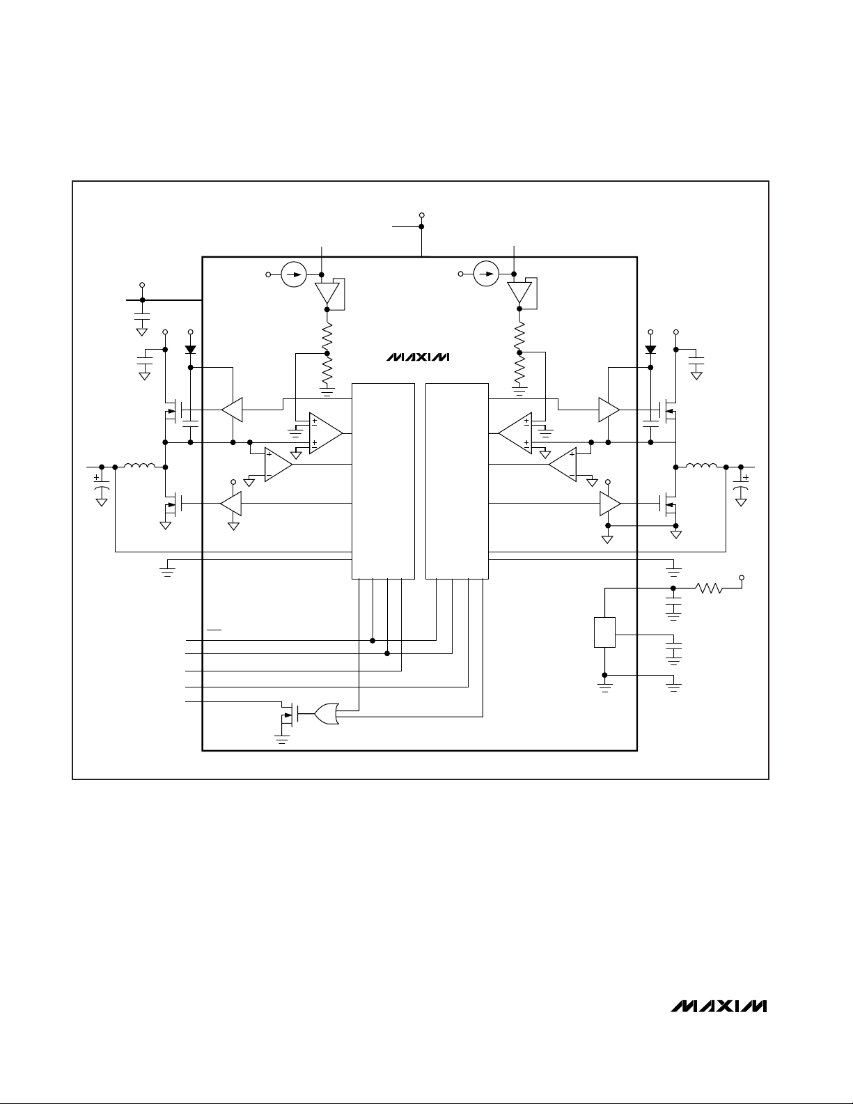
The MAX1715 buck controller is designed for low-voltage power supplies for notebook computers. Maxim’s
proprietary Quick-PWM pulse-width modulator in the
MAX1715 (Figure 2) is specifically designed for handling fast load steps while maintaining a relatively constant operating frequency and inductor operating point
over a wide range of input voltages. The Quick-PWM
architecture circumvents the poor load-transient timing
problems of fixed-frequency current-mode PWMs while
also avoiding the problems caused by widely varying
switching frequencies in conventional constant-on-time
and constant-off-time PWM schemes.
+5V Bias Supply (VCCand VDD)
The MAX1715 requires an external +5V bias supply in
addition to the battery. Typically, this +5V bias supply
is the notebook’s 95% efficient +5V system supply.
Keeping the bias supply external to the IC improves
efficiency and eliminates the cost associated with the
+5V linear regulator that would otherwise be needed to
supply the PWM circuit and gate drivers. If stand-alone
capability is needed, the +5V supply can be generated
with an external linear regulator such as the MAX1615.
Page 11
MAX1715
Ultra-High Efficiency, Dual Step-Down
Controller for Notebook Computers
______________________________________________________________________________________ 11
The power input and +5V bias inputs can be connected
together if the input source is a fixed +4.5V to +5.5V
supply. If the +5V bias supply is powered up prior to
the battery supply, the enable signal (ON1, ON2) must
be delayed until the battery voltage is present to ensure
start-up. The +5V bias supply must provide VCCand
gate-drive power, so the maximum current drawn is:
I
BIAS
= ICC+ f (QG1 + QG2) = 5mA to 30mA (typ)
where ICC is 1mA typical, f is the switching frequency,
and QG1 and QG2 are the MOSFET data sheet total
gate-charge specification limits at VGS= 5V.
Free-Running, Constant-On-Time PWM
Controller with Input Feed-Forward
The Quick-PWM control architecture is a pseudo-fixedfrequency, constant-on-time current-mode type with
voltage feed-forward (Figure 3). This architecture relies
on the output filter capacitor’s ESR to act as the current-sense resistor, so the output ripple voltage provides the PWM ramp signal. The control algorithm is
simple: the high-side switch on-time is determined solely by a one-shot whose period is inversely proportional
to input voltage and directly proportional to output voltage. Another one-shot sets a minimum off-time (400ns
typ). The on-time one-shot is triggered if the error comparator is low, the low-side switch current is below the
Table 1. Component Selection for Standard Applications
Table 2. Component Suppliers
4.75V to 5.5V7V to 20V7V to 20VInput Range
100µF, 10V
Sanyo POSCAP
10TPA100M
470µF, 4V Sanyo
POSCAP 4TPB470M
470µF, 4V Sanyo
POSCAP 4TPB470M
C2 Output Capacitor
100µF, 10V
Sanyo POSCAP
10TPA100M
10µF, 25V
Taiyo Yuden
TMK432BJ106KM
10µF, 25V
Taiyo Yuden
TMK432BJ106KM
C1 Input Capacitor
3.3µH
TOKO D73LC
3.1µH
Sumida CDRH125
4.4µH
Sumida CDRH125
L1 Inductor
—Nihon EP10QY03Nihon EP10QY03D2 Rectifier
International Rectifier
1/2 IRF7301
Fairchild
Semiconductor
1/2 FDS6982A
Fairchild
Semiconductor
1/2 FDS6982A
Q2 Low-Side MOSFET
International Rectifier
1/2 IRF7301
Fairchild
Semiconductor
1/2 FDS6982A
Fairchild
Semiconductor
1/2 FDS6982A
Q1 High-Side MOSFET
600kHz345kHz255kHz
Frequency
3.3V at 1.5A1.8V at 4A2.5V at 4ACOMPONENT
[1] 602-994-6430602-303-5454Motorola
[1] 408-986-1442408-986-0424Kemet
[1] 408-721-1635408-822-2181Fairchild Semiconductor
[1] 561-241-9339561-241-7876Coiltronics
[1] 847-639-1469847-639-6400Coilcraft
[1] 516-435-1824516-435-1110Central Semiconductor
[1] 803-626-3123803-946-0690AVX
FACTORY FAX
[Country Code]
USA PHONEMANUFACTURER
[1] 714-960-6492714-969-2491Matsuo
[1] 310-322-3332310-322-3331International Rectifier
[1] 408-573-4159408-573-4150Taiyo Yuden
[1] 603-224-1430603-224-1961Sprague
[1] 408-970-3950
408-988-8000
800-554-5565
Siliconix
[81] 7-2070-1174619-661-6835Sanyo
[81] 3-3494-7414805-867-2555*NIEC (Nihon)
[1] 814-238-0490
814-237-1431
800-831-9172
Murata
[81] 3-3607-5144847-956-0666Sumida
[1] 847-390-4405847-390-4461TDK
*Distributor
7V to 20V
(2) 470µF, 6V Kemet
T510X477108M0
06AS
(2) 10µF, 25V
Taiyo Yuden
TMK432BJ106KM
1.5µH Sumida
CEP125-1R5MC
Motorola
MBRS340T3
Fairchild
Semiconductor
FDS6670A
International
Rectifier IRF7811
255kHz
1.3V at 8A
7V to 20V
330µF, 6V AVX
TPSV337M006R
0060
10µF, 25V
Taiyo Yuden
TMK432BJ106KM
6.8µH
Coiltronics UP2B
Nihon EP10QY03
Fairchild
Semiconductor
1/2 FDS6990A
Fairchild
Semiconductor
1/2 FDS6990A
255kHz
5V at 3A
[1] 708-699-1194800-PIK-TOKOTOKO
Page 12
MAX1715
Ultra-High Efficiency, Dual Step-Down
Controller for Notebook Computers
12 ______________________________________________________________________________________
current-limit threshold, and the minimum off-time oneshot has timed out.
On-Time One-Shot (TON)
The heart of the PWM core is the one-shot that sets the
high-side switch on-time for both controllers. This fast,
low-jitter, adjustable one-shot includes circuitry that
varies the on-time in response to battery and output
voltage. The high-side switch on-time is inversely proportional to the battery voltage as measured by the V+
input, and proportional to the output voltage. This algorithm results in a nearly constant switching frequency
despite the lack of a fixed-frequency clock generator.
The benefits of a constant switching frequency are
twofold: first, the frequency can be selected to avoid
noise-sensitive regions such as the 455kHz IF band;
second, the inductor ripple-current operating point
remains relatively constant, resulting in easy design
methodology and predictable output voltage ripple.
The on-times for side 1 are set 15% higher than the
2V
REF
AGND
REF
OUT2
FB2
20Ω
PGND
V
DD
OUTPUT2
2.5V
DL2
V
CC
V
DD
LX2
ZERO
CROSSING
CURRENT
LIMIT
PWM
CONTROLLER
(SEE FIGURE 3)
DH2
BST2
R
I
LIM_
V
DD
V
CC
V+
V+
V+
OUT1
FB1
SKIP
TON
ON1
ON2
OUTPUT1
1.8V
5V INPUT
DL1
V
DD
LX1
ZERO
CROSSING
CURRENT
LIMIT
DH1
9R
R
I
LIM_
BATTERY
4.5V TO 28V
5μA
BST1
V
DD
V
DD
V
CC
V
DD
V+
PWM
CONTROLLER
(SEE FIGURE 3)
MAX1715
5μA
9R
P
GOOD
Figure 2. Functional Diagram
Page 13

MAX1715
Ultra-High Efficiency, Dual Step-Down
Controller for Notebook Computers
______________________________________________________________________________________ 13
REF
-6%
FROM
OUT
REF
FROM ZERO-CROSSING COMPARATOR
ERROR
AMP
TOFF
TON
REF
+12%
REF
-30%
FEEDBACK
MUX
(SEE FIGURE 9)
x2
OVP/UVLO
LATCH
TO DL DRIVER
TO DH DRIVER
ON-TIME
COMPUTE
TON
1-SHOT
FROM ILIM
COMPARATOR
1-SHOT
TRIG
IN
2V TO 28V
TRIG
Q
Q
S
R
FB_
OUT_
Q
S1
Q
S2 TIMER
TON
V+
S
R
Q
TO PGOOD
OR GATE
Figure 3. PWM Controller (one side only)
X = Don’t care
ON1
ON2 SKIP MODE COMMENTS
0 0 X SHUTDOWN Low-power shutdown state. DL = VDD. Clears fault latches.
0 1 X OUT1 Disable Disable OUT1. DL1 = VDD. Clears OUT1 fault latches.
1 0 X OUT2 Disable Disable OUT2. DL2 = VDD. Clears OUT2 fault latches.
X X <-0.3V No Fault Disables the output overvoltage and undervoltage fault circuitry.
1 1 V
DD
RUN (PWM)
Low Noise
Low-Noise operation with no automatic PWM/PFM switchover. Fixed-frequency PWM
action is forced regardless of load. Inductor current reverses at light load levels. I
DD
draw <1.5mA (typ) plus gate-drive current.
Table 3. Operating Mode Truth Table
1 1 AGND
RUN
(PFM/PWM)
Normal operation with automatic PWM/PFM switchover for pulse-skipping at light loads.
I
DD
<1.5mA (typ) plus gate drive current.
Page 14

MAX1715
Ultra-High Efficiency, Dual Step-Down
Controller for Notebook Computers
14 ______________________________________________________________________________________
nominal frequency setting (200kHz, 300kHz, 420kHz, or
540kHz), while the on-times for side 2 are set 15%
lower than nominal. This is done to prevent audio-frequency “beating” between the two sides, which switch
asynchronously for each side:
On-Time = K (V
OUT
+ 0.075V) / V
IN
where K is set by the TON pin-strap connection and
0.075V is an approximation to accommodate for the
expected drop across the low-side MOSFET switch.
One-shot timing error increases for the shorter on-time
settings due to fixed propagation delays; it is approximately ±12.5% at 540kHz and 420kHz nominal settings
and ±10% at the two slower settings. This translates to
reduced switching-frequency accuracy at higher frequencies (Table 5). Switching frequency increases as a
function of load current due to the increasing drop
across the low-side MOSFET, which causes a faster
inductor-current discharge ramp. The on-times guaranteed in the Electrical Characteristics are influenced by
switching delays in the external high-side power MOSFET.
Two external factors that influence switching-frequency
accuracy are resistive drops in the two conduction
loops (including inductor and PC board resistance) and
the dead-time effect. These effects are the largest contributors to the change of frequency with changing load
current. The dead-time effect increases the effective
on-time, reducing the switching frequency as one or
both dead times. It occurs only in PWM mode (SKIP =
high) when the inductor current reverses at light or negative load currents. With reversed inductor current, the
inductor’s EMF causes LX to go high earlier than normal, extending the on-time by a period equal to the
low-to-high dead time.
For loads above the critical conduction point, the actual
switching frequency is:
where V
DROP
1 is the sum of the parasitic voltage drops
in the inductor discharge path, including synchronous
rectifier, inductor, and PC board resistances; VDROP2
is the sum of the resistances in the charging path; and
tONis the on-time calculated by the MAX1715.
Automatic Pulse-Skipping Switchover
In skip mode (SKIP low), an inherent automatic
switchover to PFM takes place at light loads. This
switchover is effected by a comparator that truncates
the low-side switch on-time at the inductor current’s
zero crossing. This mechanism causes the threshold
between pulse-skipping PFM and nonskipping PWM
operation to coincide with the boundary between continuous and discontinuous inductor-current operation
(also known as the “critical conduction” point). For a
battery range of 7V to 24V, this threshold is relatively
constant, with only a minor dependence on battery voltage.
where K is the on-time scale factor (Table 5). The loadcurrent level at which PFM/PWM crossover occurs,
I
LOAD(SKIP)
, is equal to 1/2 the peak-to-peak ripple current, which is a function of the inductor value (Figure 4).
For example, in the standard application circuit with
V
OUT1
= 2.5V, VIN= 15V, and K = 2.96µs (see Table
5), switchover to pulse-skipping operation occurs at
I
LOAD
= 0.7A or about 1/6 full load. The crossover point
occurs at an even lower value if a swinging (soft-saturation) inductor is used.
The switching waveforms may appear noisy and asynchronous when light loading causes pulse-skipping
I
KV
2L
V-V
V
LOAD(SKIP)
OUT_
IN OUT
IN
≈
×
⎛
⎝
⎜
⎞
⎠
⎟
f
VV
tV V
OUT DROP
ON IN DROP
=
+
+
()
1
2
Good operating point for
compound buck designs
or desktop circuits.
+5V input540
420 3-cell Li+ notebook
Useful in 3-cell systems
for lighter loads than the
CPU core or where size is
key.
Considered mainstream
by current standards.
4-cell Li+ notebook 300
200 4-cell Li+ notebook
Use for absolute best
efficiency.
COMMENTS
TYPICAL
APPLICATION
NOMINAL
FREQUENCY
(kHz)
Table 4. Frequency Selection Guidelines
Table 5. Approximate K-Factor Errors
TON
SETTING
MIN V
IN
AT V
OUT
= 2V (V)
SIDE 1 K
FACTOR
(µs)
V
CC
2.6 4.24
OPEN 2.9 2.96
REF 3.2 2.08
GND 3.6 1.63
APPROX
K-FACTOR
ERROR (%)
±10
±10
±12.5
±12.5
SIDE 2 K
FACTOR
(µs)
5.81
4.03
2.81
2.18
Page 15

MAX1715
Ultra-High Efficiency, Dual Step-Down
Controller for Notebook Computers
______________________________________________________________________________________ 15
operation, but this is a normal operating condition that
results in high light-load efficiency. Trade-offs in PFM
noise vs. light-load efficiency are made by varying the
inductor value. Generally, low inductor values produce
a broader efficiency vs. load curve, while higher values
result in higher full-load efficiency (assuming that the
coil resistance remains fixed) and less output voltage
ripple. Penalties for using higher inductor values
include larger physical size and degraded load-transient response (especially at low input voltage levels).
DC output accuracy specifications refer to the trip level of
the error. When the inductor is in continuous conduction,
the output voltage will have a DC regulation higher than
the trip level by 50% of the ripple. In discontinuous conduction (SKIP = AGND, light-loaded), the output voltage
will have a DC regulation higher than the trip level by
approximately 1.5% due to slope compensation.
Forced-PWM Mode (
SSKKIIPP
= high)
The low-noise, forced-PWM mode (SKIP = high) disables the zero-crossing comparator, which controls the
low-side switch on-time. This causes the low-side gatedrive waveform to become the complement of the highside gate-drive waveform. This in turn causes the
inductor current to reverse at light loads as the PWM
loop strives to maintain a duty ratio of V
OUT/VIN
. The
benefit of forced-PWM mode is to keep the switching
frequency fairly constant, but it comes at a cost: the noload battery current can be 10mA to 40mA, depending
on the external MOSFETs.
Forced-PWM mode is most useful for reducing audiofrequency noise, improving load-transient response,
providing sink-current capability for dynamic output
voltage adjustment, and improving the cross-regulation
of multiple-output applications that use a flyback transformer or coupled inductor.
Current-Limit Circuit (ILIM)
The current-limit circuit employs a unique “valley” currentsensing algorithm that uses the on-state resistance of the
low-side MOSFET as a current-sensing element. If the
current-sense signal is above the current-limit threshold,
the PWM is not allowed to initiate a new cycle (Figure 5).
The actual peak current is greater than the current-limit
threshold by an amount equal to the inductor ripple current. Therefore, the exact current-limit characteristic and
maximum load capability are a function of the MOSFET
on-resistance, inductor value, and battery voltage. The
reward for this uncertainty is robust, lossless overcurrent
sensing. When combined with the undervoltage protection circuit, this current-limit method is effective in almost
every circumstance.
There is also a negative current limit that prevents excessive reverse inductor currents when V
OUT
is sinking current. The negative current-limit threshold is set to
approximately 120% of the positive current limit, and
therefore tracks the positive current limit when ILIM is
adjusted.
The current-limit threshold is adjusted with internal 5µA
current source and an external resistor at ILIM. The
current-limit threshold adjustment range is from 50mV
to 200mV, corresponding to resistor values of 100kΩ to
400kΩ. In the adjustable mode, the current-limit threshold voltage is precisely 1/10 the voltage seen at ILIM.
The threshold defaults to 100mV when ILIM is connected to V
CC
. The logic threshold for switchover to the
100mV default value is approximately VCC- 1V.
The adjustable current limit accommodates MOSFETs
with a wide range of on-resistance characteristics (see
Design Procedure).
Carefully observe the PC board layout guidelines to
ensure that noise and DC errors don’t corrupt the current-sense signals seen by LX and PGND. Mount or
Figure 4. Pulse-Skipping/Discontinuous Crossover Point
INDUCTOR CURRENT
I
LOAD
= I
PEAK
/2
ON-TIME0 TIME
-I
PEAK
L
V
BATT -VOUT
Δi
Δt
=
Figure 5. ‘‘Valley’’ Current-Limit Threshold Point
INDUCTOR CURRENT
I
LIMIT
I
LOAD
0 TIME
-I
PEAK
Page 16

MAX1715
Ultra-High Efficiency, Dual Step-Down
Controller for Notebook Computers
16 ______________________________________________________________________________________
place the IC close to the low-side MOSFET with short,
direct traces, making a Kelvin sense connection to the
source and drain terminals.
MOSFET Gate Drivers (DH, DL)
The DH and DL drivers are optimized for driving moderate-size, high-side and larger, low-side power
MOSFETs. This is consistent with the low duty factor
seen in the notebook CPU environment, where a large
V
BATT
- V
OUT
differential exists. An adaptive dead-time
circuit monitors the DL output and prevents the highside FET from turning on until DL is fully off. There must
be a low-resistance, low-inductance path from the DL
driver to the MOSFET gate for the adaptive dead-time
circuit to work properly. Otherwise, the sense circuitry
in the MAX1715 will interpret the MOSFET gate as “off”
while there is actually still charge left on the gate. Use
very short, wide traces measuring 10 to 20 squares (50
to 100 mils wide if the MOSFET is 1 inch from the
MAX1715).
The dead time at the other edge (DH turning off) is
determined by a fixed 35ns (typ) internal delay.
The internal pull-down transistor that drives DL low is
robust, with a 0.5Ω typical on-resistance. This helps
prevent DL from being pulled up during the fast risetime of the inductor node, due to capacitive coupling
from the drain to the gate of the low-side synchronousrectifier MOSFET. However, for high-current applications, you might still encounter some combinations of
high- and low-side FETs that will cause excessive gatedrain coupling, which can lead to efficiency-killing,
EMI-producing shoot-through currents. This is often
remedied by adding a resistor in series with BST,
which increases the turn-on time of the high-side FET
without degrading the turn-off time (Figure 6).
POR, UVLO, and Soft-Start
Power-on reset (POR) occurs when VCCrises above
approximately 2V, resetting the fault latch and soft-start
counter and preparing the PWM for operation. V
CC
undervoltage lockout (UVLO) circuitry inhibits switching
and forces the DL gate driver high (to enforce output
overvoltage protection) until VCCrises above 4.2V,
whereupon an internal digital soft-start timer begins to
ramp up the maximum allowed current limit. The ramp
occurs in five steps: 20%, 40%, 60%, 80%, and 100%;
100% current is available after 1.7ms ±50%.
A continuously adjustable analog soft-start function can
be realized by adding a capacitor in parallel with the
ILIM external resistor. This soft-start method requires a
minimum interval between power-down and power-up
to discharge the capacitor.
Power-Good Output (PGOOD)
The output voltage is continuously monitored for undervoltage by the PGOOD comparator. In shutdown, softstart, and standby modes, PGOOD is actively held low.
After digital soft-start has terminated, PGOOD is
released if both the outputs are within 5.5% of the error
comparator threshold. The PGOOD output is a true
open-drain type with no parasitic ESD diodes. Note
that the PGOOD undervoltage detector is completely
independent of the output UVP fault detector.
Output Overvoltage Protection (OVP)
The overvoltage protection circuit is designed to protect against a shorted high-side MOSFET by drawing
high current and blowing the battery fuse. The output
voltage is continuously monitored for overvoltage. If the
output is more than 10.5% above the trip level of the
error amplifier, OVP is triggered and the circuit shuts
down. The DL low-side gate-driver output is then
latched high until SHDN is toggled or V
CC
power is
cycled below 1V. This action turns on the synchronousrectifier MOSFET with 100% duty and, in turn, rapidly
discharges the output filter capacitor and forces the
output to ground. If the condition that caused the overvoltage (such as a shorted high-side MOSFET) persists, the battery fuse will blow. DL is also kept high
continuously when VCCUVLO is active, as well as in
shutdown mode (Table 3).
Note that DL latching high causes the output voltage to
go slightly negative, due to energy stored in the output
LC at the instant OVP activates. If the load can’t tolerate being forced to a negative voltage, it may be desirable to place a power Schottky diode across the output
to act as a reverse-polarity clamp (Figure 1).
BST
+5V
V
IN
5Ω
DH
LX
MAX1715
Figure 6. Reducing the Switching-Node Rise Time
Page 17
MAX1715
Ultra-High Efficiency, Dual Step-Down
Controller for Notebook Computers
______________________________________________________________________________________ 17
Overvoltage protection can be defeated through the
SKIP test mode (Table 3).
Output Undervoltage Protection (UVP)
The output undervoltage protection function is similar to
foldback current limiting, but employs a timer rather
than a variable current limit. If the MAX1715 output voltage is under 70% of the nominal value 20ms after coming out of shutdown, the PWM is latched off and won’t
restart until VCCpower is cycled or SHDN is toggled.
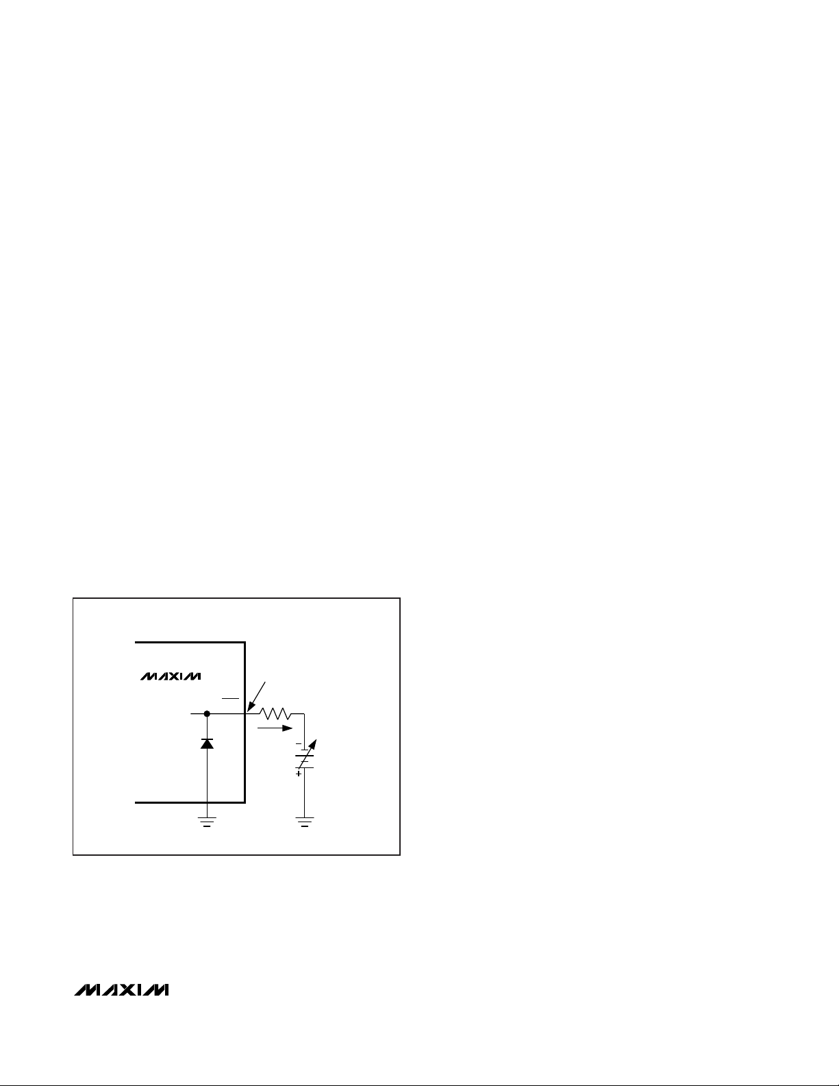
No-Fault Test Mode
The over/undervoltage protection features can complicate the process of debugging prototype breadboards
since there are (at most) a few milliseconds in which to
determine what went wrong. Therefore, a test mode is
provided to totally disable the OVP, UVP, and thermal
shutdown features, and clear the fault latch if it has
been set. The PWM operates as if SKIP were grounded
(PFM/PWM mode).
The no-fault test mode is entered by sinking 1.5mA
from SKIP through an external negative voltage source
in series with a resistor (Figure 7). SKIP is clamped to
AGND with a silicon diode, so choose the resistor value
equal to (V
FORCE
- 0.65V) / 1.5mA.
__________________Design Procedure
Firmly establish the input voltage range and maximum
load current before choosing a switching frequency
and inductor operating point (ripple-current ratio). The
primary design trade-off lies in choosing a good switching frequency and inductor operating point, and the following four factors dictate the rest of the design:
1) Input voltage range. The maximum value (V
IN(MAX)
)
must accommodate the worst-case high AC adapter
voltage. The minimum value (V
IN(MIN)
) must account
for the lowest battery voltage after drops due to connectors, fuses, and battery selector switches. If
there is a choice at all, lower input voltages result in
better efficiency.
2) Maximum load current. There are two values to
consider. The peak load current (I
LOAD(MAX)
) determines the instantaneous component stresses and filtering requirements, and thus drives output
capacitor selection, inductor saturation rating, and
the design of the current-limit circuit. The continuous
load current (I
LOAD
) determines the thermal stresses
and thus drives the selection of input capacitors,
MOSFETs, and other critical heat-contributing components. Modern notebook CPUs generally exhibit
I
LOAD
= I
LOAD(MAX)
· 80%.
3) Switching frequency. This choice determines the
basic trade-off between size and efficiency. The
optimal frequency is largely a function of maximum
input voltage, due to MOSFET switching losses that
are proportional to frequency and V
IN
2
. The optimum frequency is also a moving target, due to rapid
improvements in MOSFET technology that are making higher frequencies more practical (Table 4).
4) Inductor operating point. This choice provides
trade-offs between size vs. efficiency. Low inductor
values cause large ripple currents, resulting in the
smallest size, but poor efficiency and high output
noise. The minimum practical inductor value is one
that causes the circuit to operate at the edge of critical conduction (where the inductor current just
touches zero with every cycle at maximum load).
Inductor values lower than this grant no further sizereduction benefit.
The MAX1715’s pulse-skipping algorithm initiates
skip mode at the critical conduction point. So, the
inductor operating point also determines the loadcurrent value at which PFM/PWM switchover occurs.
The optimum point is usually found between 20%
and 50% ripple current.
APPROXIMATELY
-0.65V
1.5mA
V
FORCE
SKIP
AGND
MAX1715
Figure 7. Disabling Over/Undervoltage Protection (Test Mode)
Page 18

MAX1715
Ultra-High Efficiency, Dual Step-Down
Controller for Notebook Computers
18 ______________________________________________________________________________________
The inductor ripple current also impacts transientresponse performance, especially at low VIN- V
OUT
differentials. Low inductor values allow the inductor
current to slew faster, replenishing charge removed
from the output filter capacitors by a sudden load step.
The amount of output sag is also a function of the maximum duty factor, which can be calculated from the ontime and minimum off-time:
where
where minimum off-time = 400ns typ (see Table 5).
Inductor Selection
The switching frequency (on-time) and operating point
(% ripple or LIR) determine the inductor value as follows:
Example: I
LOAD(MAX)
= 8A, VIN= 7V, V
OUT
= 1.6V, f =
300kHz, 35% ripple current or LIR = 0.35:
Find a low-loss inductor having the lowest possible DC
resistance that fits in the allotted dimensions. Ferrite
cores are often the best choice; although powdered
iron is inexpensive and can work well at 200kHz. The
core must be large enough not to saturate at the peak
inductor current (I
PEAK
):
I
PEAK
= I
LOAD(MAX)
+ [(LIR / 2) ✕I
LOAD(MAX)
]
Determining the Current Limit
The minimum current-limit threshold must be great
enough to support the maximum load current when the
current limit is at the minimum tolerance value. The valley of the inductor current occurs at I
LOAD(MAX)
minus
half of the ripple current; therefore:
I
LIMIT(LOW)
> I
LOAD(MAX)
- (LIR / 2) I
LOAD(MAX)
where I
LIMIT(LOW)
= minimum current-limit threshold
voltage divided by the R
DS(ON)
of Q2. For the
MAX1715, the minimum current-limit threshold (100mV
default setting) is 90mV. Use the worst-case maximum
value for R
DS(ON)
from the MOSFET Q2 data sheet, and
add some margin for the rise in R
DS(ON)
with tempera-
ture. A good general rule is to allow 0.5% additional
resistance for each °C of temperature rise.
Examining the 8A circuit example with a maximum
R
DS(ON)
= 12mΩ at high temperature reveals the fol-
lowing:
I
LIMIT(LOW)
= 90mV / 12mΩ = 7.5A
7.5A is greater than the valley current of 6.6A, so the
circuit can easily deliver the full-rated 8A using the
default 100mV nominal ILIM threshold.
Output Capacitor Selection
The output filter capacitor must have low enough effective series resistance (ESR) to meet output ripple and
load-transient requirements, yet have high enough ESR
to satisfy stability requirements. Also, the capacitance
value must be high enough to absorb the inductor
energy going from a full-load to no-load condition without tripping the overvoltage protection circuit.
In CPU V
CORE
converters and other applications where
the output is subject to violent load transients, the output capacitor’s size depends on how much ESR is
needed to prevent the output from dipping too low
under a load transient. Ignoring the sag due to finite
capacitance:
In non-CPU applications, the output capacitor’s size
depends on how much ESR is needed to maintain an
acceptable level of output voltage ripple:
The actual microfarad capacitance value required
relates to the physical size needed to achieve low ESR,
as well as to the chemistry of the capacitor technology.
Thus, the capacitor is usually selected by ESR and voltage rating rather than by capacitance value (this is true
of tantalums, OS-CONs, and other electrolytics).
When using low-capacity filter capacitors such as
ceramic or polymer types, capacitor size is usually
determined by the capacity needed to prevent VSAG
and VSOAR from causing problems during load transients. Also, the capacitance must be great enough to
prevent the inductor’s stored energy from launching the
output above the overvoltage protection threshold.
Generally, once enough capacitance is added to meet
the overshoot requirement, undershoot at the rising
load edge is no longer a problem (see the VSAG equation in the Design Procedure).
R
Vp p
LIR I
ESR
LOAD MAX
≤
×-
()
R
V
I
ESR
DIP
LOAD MAX
≤
()
L
1.6V (7 - 1 6)
7 300kHz 0.33 8A
1.6 H =
×
×××
=μ
L =
V(V- V)
V f LIR I
OUT IN OUT
IN LOAD(MAX)
×× ×
DUTY
K (V + 0.075V) V
K (V + 0.075V) V + min off -time
OUT IN
OUT OUT
=
V
IL
C DUTY V V
SAG
LOAD MAX
F IN MIN OUT
=
×
××
()
()
()
()
Δ
-
2
2
Page 19

MAX1715
Ultra-High Efficiency, Dual Step-Down
Controller for Notebook Computers
______________________________________________________________________________________ 19
The amount of overshoot due to stored inductor energy
can be calculated as:
where I
PEAK
is the peak inductor current.
Output Capacitor Stability Considerations
Stability is determined by the value of the ESR zero relative to the switching frequency. The point of instability
is given by the following equation:
where:
For a typical 300kHz application, the ESR zero frequency must be well below 95kHz, preferably below 50kHz.
Tantalum and OS-CON capacitors in widespread use
at the time of publication have typical ESR zero frequencies of 15kHz. In the design example used for
inductor selection, the ESR needed to support 50mVp-p
ripple is 50mV/3.5A = 14.2mΩ. Three 470µF/4V Kemet
T510 low-ESR tantalum capacitors in parallel provide
15mΩ max ESR. Their typical combined ESR results in
a zero at 14.1kHz, well within the bounds of stability.
Don’t put high-value ceramic capacitors directly across
the fast feedback inputs (FB_ to AGND) without taking
precautions to ensure stability. Large ceramic capacitors can have a high-ESR zero frequency and cause
erratic, unstable operation. However, it’s easy to add
enough series resistance by placing the capacitors a
couple of inches downstream from the junction of the
inductor and FB_ pin (see the All-Ceramic-Capacitor
Application section).
Unstable operation manifests itself in two related but
distinctly different ways: double-pulsing and fast-feedback loop instability.
Double-pulsing occurs due to noise on the output or
because the ESR is so low that there isn’t enough voltage ramp in the output voltage signal. This “fools” the
error comparator into triggering a new cycle immediately after the 400ns minimum off-time period has
expired. Double-pulsing is more annoying than harmful,
resulting in nothing worse than increased output ripple.
However, it can indicate the possible presence of loop
instability, which is caused by insufficient ESR.
Loop instability can result in oscillations at the output
after line or load perturbations that can trip the overvoltage protection latch or cause the output voltage to fall
below the tolerance limit.
The easiest method for checking stability is to apply a
very fast zero-to-max load transient (refer to the
MAX1715 EV kit manual) and carefully observe the output voltage ripple envelope for overshoot and ringing. It
can help to simultaneously monitor the inductor current
with an AC current probe. Don’t allow more than one
cycle of ringing after the initial step-response under- or
overshoot.
Input Capacitor Selection
The input capacitor must meet the ripple current
requirement (IRMS) imposed by the switching currents.
Nontantalum chemistries (ceramic, aluminum, or OSCON) are preferred due to their resistance to power up
surge currents.
Power MOSFET Selection
Most of the following MOSFET guidelines focus on the
challenge of obtaining high load-current capability
(>5A) when using high-voltage (>20V) AC adapters.
Low-current applications usually require less attention.
For maximum efficiency, choose a high-side MOSFET
(Q1) that has conduction losses equal to the switching
losses at the optimum battery voltage (15V). Check to
ensure that the conduction losses at the minimum
input voltage don’t exceed the package thermal limits
or violate the overall thermal budget. Check to ensure
that conduction losses plus switching losses at the
maximum input voltage don’t exceed the package ratings or violate the overall thermal budget.
Choose a low-side MOSFET (Q2) that has the lowest
possible R
DS(ON)
, comes in a moderate to small package (i.e., SO-8), and is reasonably priced. Ensure that
the MAX1715 DL gate driver can drive Q2; in other
words, check that the gate isn’t pulled up by the highside switch turning on due to parasitic drain-to-gate
capacitance, causing cross-conduction problems.
Switching losses aren’t an issue for the low-side MOSFET since it’s a zero-voltage switched device when
used in the buck topology.
MOSFET Power Dissipation
Worst-case conduction losses occur at the duty factor
extremes. For the high-side MOSFET, the worst-case-
I I
VV-V
V
RMS LOAD
OUT IN OUT
IN
=
()
⎛
⎝
⎜
⎜
⎞
⎠
⎟
⎟
f
RC
ESR
ESR F
=
×× ×
1
2 π
f
f
ESR
=
π
ΔV
LI
2
2CV
PEAK
OUT
≈
Page 20

MAX1715
Ultra-High Efficiency, Dual Step-Down
Controller for Notebook Computers
20 ______________________________________________________________________________________
power dissipation (PD) due to resistance occurs at
minimum battery voltage:
Generally, a small high-side MOSFET is desired in
order to reduce switching losses at high input voltages.
However, the R
DS(ON)
required to stay within package
power-dissipation limits often limits how small the MOSFET can be. Again, the optimum occurs when the
switching (AC) losses equal the conduction (R
DS(ON)
)
losses. High-side switching losses don’t usually
become an issue until the input is greater than approximately 15V.
Switching losses in the high-side MOSFET can become
an insidious heat problem when maximum AC adapter
voltages are applied, due to the squared term in the
CV2F switching loss equation. If the high-side MOSFET
you’ve chosen for adequate R
DS(ON)
at low battery
voltages becomes extraordinarily hot when subjected
to V
IN(MAX)
, reconsider your choice of MOSFET.
Calculating the power dissipation in Q1 due to switching losses is difficult since it must allow for difficult
quantifying factors that influence the turn-on and turnoff times. These factors include the internal gate resistance, gate charge, threshold voltage, source
inductance, and PC board layout characteristics. The
following switching loss calculation provides only a
very rough estimate and is no substitute for breadboard evaluation, preferably including a verification
using a thermocouple mounted on Q1:
where C
RSS
is the reverse transfer capacitance of Q1
and I
GATE
is the peak gate-drive source/sink current
(1A typ).
For the low-side MOSFET, Q2, the worst-case power
dissipation always occurs at maximum battery voltage:
The absolute worst case for MOSFET power dissipation
occurs under heavy overloads that are greater than
I
LOAD(MAX)
but are not quite high enough to exceed
the current limit and cause the fault latch to trip. To protect against this possibility, you must “overdesign” the
circuit to tolerate:
I
LOAD
= I
LIMIT(HIGH)
+ (LIR / 2) ✕I
LOAD(MAX)
where I
LIMIT(HIGH)
is the maximum valley current
allowed by the current-limit circuit, including threshold
tolerance and on-resistance variation. This means that
the MOSFETs must be very well heatsinked. If short-circuit protection without overload protection is enough, a
normal I
LOAD
value can be used for calculating com-
ponent stresses.
Choose a Schottky diode (D1) having a forward voltage
low enough to prevent the Q2 MOSFET body diode
from turning on during the dead time. As a general
rule, a diode having a DC current rating equal to 1/3 of
the load current is sufficient. This diode is optional and
can be removed if efficiency isn’t critical.
_________________Application Issues
Dropout Performance
The output voltage adjust range for continuous-conduction operation is restricted by the nonadjustable
500ns (max) minimum off-time one-shot. For best
dropout performance, use the slowest (200kHz) ontime setting. When working with low input voltages, the
duty-factor limit must be calculated using worst-case
values for on- and off-times. Manufacturing tolerances
and internal propagation delays introduce an error to
the TON K-factor. This error is greater at higher frequencies (Table 5). Also, keep in mind that transient
response performance of buck regulators operated
close to dropout is poor, and bulk output capacitance
must often be added (see the VSAG equation in the
Design Procedure).
Dropout design example: VIN= 3V min, V
OUT
= 2V, f
= 300kHz. The required duty is (V
OUT
+ VSW) / (VINVSW) = (2V + 0.1V) / (3.0V - 0.1V) = 72.4%. The worstcase on-time is (V
OUT
+ 0.075) / V
IN
✕
K = 2.075V / 3V
✕
3.35µs-V ✕90% = 2.08µs. The IC duty-factor limitation
is:
which meets the required duty.
Remember to include inductor resistance and MOSFET
on-state voltage drops (VSW) when doing worst-case
dropout duty-factor calculations.
All-Ceramic-Capacitor Application
Ceramic capacitors have advantages and disadvantages. They have ultra-low ESR and are noncombustible, relatively small, and nonpolarized. They are
also expensive and brittle, and their ultra-low ESR characteristic can result in excessively high ESR zero frequencies (affecting stability). In addition, their relatively
low capacitance value can cause output overshoot
DUTY
t
tt
2.08 s
2.08 s 500ns
80.6%
ON(MIN)
ON(MIN) OFF(MAX)
=
+
=
+
=
μ
μ
PD(Q2)
1 - V
V
I R
OUT
IN MAX
LOAD
2
DS ON
=
⎛
⎝
⎜
⎜
⎞
⎠
⎟
⎟
×
()
()
PD(Q1 switching)
CV fI
I
RSS IN(MAX)
2
LOAD
GATE
=
×××
PD(Q1 resistance)
V
V
I R
OUT
IN MIN
LOAD
2
DS ON
=
⎛
⎝
⎜
⎜
⎞
⎠
⎟
⎟
×
()
()
Page 21

MAX1715
Ultra-High Efficiency, Dual Step-Down
Controller for Notebook Computers
______________________________________________________________________________________ 21
when going abruptly from full-load to no-load conditions, unless there are some bulk tantalum or electrolytic capacitors in parallel to absorb the stored energy in
the inductor. In some cases, there may be no room for
electrolytics, creating a need for a DC-DC design that
uses nothing but ceramics.
The all-ceramic-capacitor application of Figure 8
replaces the standard tantalum output capacitors with
ceramics. This design relies on having a minimum of
5mΩ parasitic PC board trace resistance in series with
the capacitor to reduce the ESR zero frequency. This
small amount of resistance is easily obtained by locating the MAX1714A circuit 2 or 3 inches away from the
CPU, and placing all the ceramic capacitors close to
the CPU. Resistance values higher than 5mΩ just
improve the stability (which can be observed by examining the load-transient response characteristic as
shown in the Typical Operating Characteristics). Avoid
adding excess PC board trace resistance, as there’s an
efficiency penalty; 5mΩ is sufficient for a 7A circuit:
Output overshoot (ΔV) determines the minimum output
capacitance requirement. In this example, the switching frequency has been increased to 600kHz and the
inductor value has been reduced to 0.5µH (compared
to 300kHz and 2µH for the standard 8A circuit) to minimize the energy transferred from inductor to capacitor
during load-step recovery. The overshoot must be calculated to avoid tripping the OVP latch. The efficiency
penalty for operating at 540kHz is about 2% to 3%,
depending on the input voltage.
An optional 1Ω resistor is placed in series with OUT.
This resistor attenuates high-frequency noise in some
bands, which causes double pulsing.
Fixed Output Voltages
The MAX1715’s Dual Mode™ operation allows the
selection of common voltages without requiring external
components (Figure 9). Connect FB to AGND for a
fixed +2.5V output or to VCCfor a +3.3V output, or connect FB directly to OUT for a fixed +1.0V output.
Setting V
OUT
with a Resistor-Divider
The output voltage can be adjusted with a resistordivider if desired (Figure 8). The equation for adjusting
the output voltage is:
where VFBis 1.0V and R2 is about 10kΩ.
Two-Stage (5V-Powered) Notebook
CPU Buck Regulator
The most efficient and overall cost-effective solution for
stepping down a high-voltage battery to a very low output voltage is to use a single-stage buck regulator
that’s powered directly from the battery. However, there
may be situations where the battery bus can’t be routed
near the CPU, or where space constraints dictate the
smallest possible local DC-DC converter. In such
cases, the 5V-powered circuit of Figure 10 may be
appropriate. The reduced input voltage allows a higher
V V 1
R1
R2
OUT FB
=+
⎛
⎝
⎜
⎞
⎠
⎟
R
1
2FC
ESR
OUT
≥
MAX1715
TO ERROR
AMP1
TO ERROR
AMP2
OUT2
FB2
0.2V
0.2V
2V
FB1
FIXED
2.5V
FIXED
1.8V
FIXED
3.3V
OUT1
Figure 9. Feedback Mux
DL
AGND
OUT
PGND
DH
1/2
FB
V
BATT
V
OUT
R1
R2
MAX1715
Figure 8. Setting V
OUT
with a Resistor-Divider
Dual Mode is a trademark of Maxim Integrated Products.
Page 22

MAX1715
Ultra-High Efficiency, Dual Step-Down
Controller for Notebook Computers
22 ______________________________________________________________________________________
switching frequency and a much smaller inductor
value.
PC Board Layout Guidelines
Careful PC board layout is critical to achieving low
switching losses and clean, stable operation. This is
especially true for dual converters, where one channel
can affect the other. The switching power stages require
particular attention (Figure 11). Refer to the MAX1715
EV kit data sheet for a specific layout example.
If possible, mount all of the power components on the
top side of the board with their ground terminals flush
against one another. Follow these guidelines for good
PC board layout:
• Isolate the power components on the top side from
the sensitive analog components on the bottom side
with a ground shield. Use a separate PGND plane
under the OUT1 and OUT2 sides (called PGND1 and
PGND2). Avoid the introduction of AC currents into
the PGND1 and PGND2 ground planes. Run the
power plane ground currents on the top side only, if
possible.
• Use a star ground connection on the power plane to
minimize the crosstalk between OUT1 and OUT2.
• Keep the high-current paths short, especially at the
ground terminals. This practice is essential for stable, jitter-free operation.
• Tie AGND and PGND together close to the IC. Do
not connect them together anywhere else. Carefully
follow the grounding instructions under Step 4 of the
Layout Procedure.
• Keep the power traces and load connections short.
This practice is essential for high efficiency. Using
thick copper PC boards (2oz vs. 1oz) can enhance
full-load efficiency by 1% or more. Correctly routing
PC board traces is a difficult task that must be
approached in terms of fractions of centimeters,
where a single milliohm of excess trace resistance
causes a measurable efficiency penalty.
• LX_ and PGND connections to the synchronous rectifiers for current limiting must be made using Kelvin
sense connections to guarantee the current-limit
accuracy. With SO-8 MOSFETs, this is best done by
routing power to the MOSFETs from outside using
the top copper layer, while tying in PGND and LX_
inside (underneath) the SO-8 package.
• When trade-offs in trace lengths must be made, it’s
preferable to allow the inductor charging path to be
ILIM V
CC
V
IN
4.5V TO 5.5V
L1
0.5μH
V
OUT
2.5V AT 7A
ON2
1μF
0.1μF
0.22μF
C2
3 x 470μF
KEMET T510
IRF7805
IRF7805
1μF20Ω
C1
4 x 10μF/25V
ON/OFF
DL2
LX2
BST2
DH2
PGND
OUT2
FB2
AGND
V
DD
V
CC
V+
MAX1715
REF
TON
SKIP
100k
PGOOD
Figure 10. 5V-Powered, 8A CPU Buck Regulator
Page 23

MAX1715
Ultra-High Efficiency, Dual Step-Down
Controller for Notebook Computers
______________________________________________________________________________________ 23
made longer than the discharge path. For example,
it’s better to allow some extra distance between the
input capacitors and the high-side MOSFET than to
allow distance between the inductor and the lowside MOSFET or between the inductor and the output filter capacitor.
• Ensure that the OUT connection to C
OUT
is short and
direct. However, in some cases it may be desirable
to deliberately introduce some trace length between
the OUT inductor node and the output filter capacitor
(see the All-Ceramic-Capacitor Application section).
• Route high-speed switching nodes (BST_, LX_, DH_,
and DL_) away from sensitive analog areas (REF,
ILIM, FB). Use PGND1 and PGND2 as EMI shields to
keep radiated switching noise away from the IC,
feedback dividers, and analog bypass capacitors.
• Make all pin-strap control input connections (SKIP,
ILIM, etc.) to AGND or VCCrather than PGND_or
VDD.
Layout Procedure
1) Place the power components first, with ground terminals adjacent (Q2 source, C
IN
-, C
OUT
-, D1 anode). If
possible, make all these connections on the top
layer with wide, copper-filled areas.
2) Mount the controller IC adjacent to the synchronous
rectifiers MOSFETs, preferably on the back side in
order to keep LX_, PGND_, and the DL_ gate-drive
line short and wide. The DL_ gate trace must be
short and wide, measuring 10 to 20 squares (50mils
to 100mils wide if the MOSFET is 1 inch from the
controller IC).
3) Group the gate-drive components (BST_ diode and
capacitor, VDDbypass capacitor) together near the
controller IC.
4) Make the DC-DC controller ground connections as
follows: near the IC, create a small analog ground
plane. Connect this plane to AGND and use this
plane for the ground connection for the REF and
V
CC
bypass capacitors, FB dividers, and I
LIM
resistors (if any). Create another small ground island for
PGND, and use it for the VDDbypass capacitor,
placed very close to the IC. Connect the AGND and
the PGND pins together under the IC (this is the only
connection between AGND and PGND).
5) On the board’s top side (power planes), make a star
ground to minimize crosstalk between the two sides.
The top-side star ground is a star connection of the
input capacitors, side 1 low-side MOSFET, and side
2 low-side MOSFET. Keep the resistance low
between the star ground and the source of the lowside MOSFETs for accurate current limit. Connect
the top-side star ground (used for MOSFET, input,
and output capacitors) to the small PGND island with
a short, wide connection (preferably just a via).
If multiple layers are available (highly recommended), create PGND1 and PGND2 islands on the layer
just below the top-side layer (refer to the MAX1715
EV kit for an example) to act as an EMI shield.
Connect each of these individually to the star ground
via, which connects the top side to the PGND plane.
Add one more solid ground plane under the IC to act
as an additional shield, and also connect that to the
star ground via.
6) Connect the output power planes (V
CORE
and system ground planes) directly to the output filter
capacitor positive and negative terminals with multiple vias.
AGND
PGND
VIA TO OUT1
GROUND
OUT2OUT1
VIA TO OUT2
VIA TO PGND
VIA TO LX1
V
IN
VIA TO LX2
USE AGND PLANE TO:
- BYPASS V
CC
AND REF
- TERMINATE EXTERNAL FB
DIVIDER (IF USED)
- TERMINATE R
ILIM
(IF USED)
- PIN-STRAP CONTROL
INPUTS
USE PGND PLANE TO:
- BYPASS V
DD
- CONNECT PGND TO THE TOPSIDE STAR GROUND
VIA TO GROUND
NOTE: EXAMPLE SHOWN IS FOR DUAL N-CHANNEL MOSFET.
CONNECT PGND TO AGND
BENEATH THE MAX1715 AT
ONE POINT ONLY AS SHOWN.
C4
C3
C1
N1
D1
D2
N2
C2
L1
L2
Figure 11. PC Board Layout Example
Page 24

MAX1715
Ultra-High Efficiency, Dual Step-Down
Controller for Notebook Computers
24 ______________________________________________________________________________________
Pin Configuration
28
27
26
25
24
23
22
21
20
19
18
17
16
15
1
2
3
4
5
6
7
8
9
10
11
12
13
14
N.C.
LX1
DH1
BST1
DL1
N.C.
N.C.
PGND
V
CC
V
DD
DL2
BST2
DH2
LX2
OUT2
FB2
ILIM2
ON2
ON1
REF
AGND
PGOOD
SKIP
TON
V+
ILIM1
FB1
OUT1
QSOP
TOP VIEW
MAX1715
Page 25

Ultra-High Efficiency, Dual Step-Down
Controller for Notebook Computers
MAX1715
Maxim cannot assume responsibility for use of any circuitry other than circuitry entirely embodied in a Maxim product. No circuit patent licenses are
implied. Maxim reserves the right to change the circuitry and specifications without notice at any time.
25 ____________________Maxim Integrated Products, 120 San Gabriel Drive, Sunnyvale, CA 94086 408-737-7600
© 2005 Maxim Integrated Products Printed USA is a registered trademark of Maxim Integrated Products, Inc.
QSOP.EPS
Package Information
(The package drawing(s) in this data sheet may not reflect the most current specifications. For the latest package outline information
go to www.maxim-ic.com/packages
.)
 Loading...