

For free samples & the latest literature: http://www.maxim-ic.com, or phone 1-800-998-8800
For small orders, phone 1-800-835-8769.
General Description
The MAX1710/MAX1711 step-down controllers are
intended for core CPU DC-DC converters in notebook
computers. They feature a triple-threat combination of
ultra-fast transient response, high DC accuracy, and
high efficiency needed for leading-edge CPU core
power supplies. Maxim’s proprietary QUICK-PWM™
quick-response, constant-on-time PWM control scheme
handles wide input/output voltage ratios with ease and
provides 100ns “instant-on” response to load transients
while maintaining a relatively constant switching frequency.
High DC precision is ensured by a 2-wire remote-sensing scheme that compensates for voltage drops in both
ground bus and the supply rail. An on-board, digital-toanalog converter (DAC) sets the output voltage in compliance with Mobile Pentium II®CPU specifications.
The MAX1710 achieves high efficiency at a reduced
cost by eliminating the current-sense resistor found in
traditional current-mode PWMs. Efficiency is further
enhanced by an ability to drive very large synchronousrectifier MOSFETs.
Single-stage buck conversion allows these devices to
directly step down high-voltage batteries for the highest
possible efficiency. Alternatively, 2-stage conversion
(stepping down the +5V system supply instead of the
battery) at a higher switching frequency allows the minimum possible physical size.
The MAX1710 and MAX1711 are identical except that
the MAX1711 has a 5-bit DAC rather than a 4-bit DAC.
Also, the MAX1711 has a fixed overvoltage protection
threshold at V
OUT
= 2.25V and undervoltage protection
at V
OUT
= 0.8V, whereas the MAX1710 has variable
thresholds that track V
OUT
. The MAX1711 is intended
for applications where the DAC code may change
dynamically.
Applications
Notebook Computers
Docking Stations
CPU Core DC-DC Converters
Single-Stage (BATT to V
CORE)
Converters
Two-Stage (+5V to V
CORE
) Converters
Features
♦ Ultra-High Efficiency
♦ No Current-Sense Resistor (Lossless I
LIMIT
)
♦ QUICK-PWM with 100ns Load-Step Response
♦ ±1% V
OUT
Accuracy over Line and Load
♦ 4-Bit On-Board DAC (MAX1710)
♦ 5-Bit On-Board DAC (MAX1711)
♦ 0.925V to 2V Output Adjust Range (MAX1711)
♦ 2V to 28V Battery Input Range
♦ 200/300/400/550kHz Switching Frequency
♦ Remote GND and V
OUT
Sensing
♦ Over/Undervoltage Protection
♦ 1.7ms Digital Soft-Start
♦ Drives Large Synchronous-Rectifier FETs
♦ 2V ±1% Reference Output
♦ Power-Good Indicator
♦ Small 24-Pin QSOP Package
MAX1710/MAX1711
High-Speed, Digitally Adjusted
Step-Down Controllers for Notebook CPUs
________________________________________________________________
Maxim Integrated Products
1
19-4781; Rev 0; 11/98
Pin Configuration appears at end of data sheet.
QUICK-PWM is a trademark of Maxim Integrated Products.
Mobile Pentium II is a registered trademark of Intel Corp.
-40°C to +85°C
PART
MAX1710EEG
TEMP. RANGE PIN-PACKAGE
24 QSOP
Ordering Information
MAX1711EEG -40°C to +85°C 24 QSOP
EVALUATION KIT MANUAL
FOLLOWS DATA SHEET
SKIP
GND
DH
LX
DL
BST
+5V INPUT
ILIM
GNDS
FBS
D0
D1
D2
D3
D4**
*MAX1710 ONLY
**MAX1711 ONLY
REF
CC
PGND
FB
MAX1710
MAX1711
V+
V
CC
OVP* V
DD
SHDN
OUTPUT
0.925V TO 2V
(MAX1711)
D/A
INPUTS
BATTERY
4.5V TO 28V
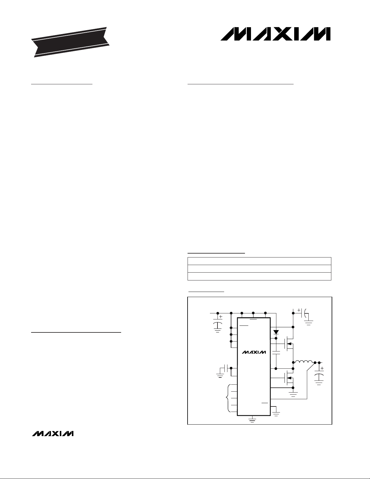
Minimal Operating Circuit
MAX1710/MAX1711
High-Speed, Digitally Adjusted
Step-Down Controllers for Notebook CPUs
2 _______________________________________________________________________________________
ABSOLUTE MAXIMUM RATINGS
Stresses beyond those listed under “Absolute Maximum Ratings” may cause permanent damage to the device. These are stress ratings only, and functional
operation of the device at these or any other conditions beyond those indicated in the operational sections of the specifications is not implied. Exposure to
absolute maximum rating conditions for extended periods may affect device reliability.
V+ to GND..............................................................-0.3V to +30V
V
CC
, VDDto GND.....................................................-0.3V to +6V
PGND to GND.....................................................................±0.3V
SHDN, PGOOD to GND ...........................................-0.3V to +6V
OVP, ILIM, FB, FBS, CC, REF, D0–D4,
GNDS, TON to GND..............................-0.3V to (V
CC
+ 0.3V)
SKIP to GND (Note 1).................................-0.3V to (V
CC
+ 0.3V)
DL to PGND................................................-0.3V to (V
DD
+ 0.3V)
BST to GND............................................................-0.3V to +36V
DH to LX.....................................................-0.3V to (BST + 0.3V)
LX to BST..................................................................-6V to +0.3V
REF Short Circuit to GND...........................................Continuous
Continuous Power Dissipation (T
A
= +70°C)
24-Pin QSOP (derate 9.5mW/°C above +70°C)..........762mW
Operating Temperature Range ...........................-40°C to +85°C
Junction Temperature......................................................+150°C
Storage Temperature Range.............................-65°C to +165°C
Lead Temperature (soldering, 10sec).............................+300°C
V
BATT
= 4.5V to 28V, includes
load regulation error
SHDN = 0, measured at V+ = 28V, VCC= VDD= 0 or 5V
SHDN = 0
V
CC,VDD
SHDN = 0
Battery voltage, V+
Measured at V+
Measured at VDD, FB forced above the regulation point
Measured at VCC, FB forced above the regulation point
Rising edge of SHDN to full I
LIM
(Note 2)
V
BATT
= 24V,
FB = 2V
(Note 2)
FB (MAX1710 only) or FBS
FB-FBS or GNDS-GND = 0 to 25mV
VCC= 4.5V to 5.5V, V
BATT
= 4.5V to 28V
CONDITIONS
µA<1 5
Shutdown Battery Supply
Current
µA<1 5Shutdown Supply Current (VDD)
µA<1 5Shutdown Supply Current (VCC)
µA25 40Quiescent Battery Supply Current
µA<1 5Quiescent Supply Current (VDD)
µA600 950Quiescent Supply Current (VCC)
ns400 500Minimum Off-Time
380 425 470
260 290 320
175 200 225
%
-1 1
DC Output Voltage Accuracy
TON = REF (400kHz)
4.5 5.5
V
2 28
Input Voltage Range
TON = GND (550kHz)
ns
140 160 180
On-Time
ms1.7Soft-Start Ramp Time
µA-1 1GNDS Input Bias Current
µA-0.2 0.2FB Input Bias Current
TON = open (300kHz)
mV3Remote Sense Voltage Error
mV5Line Regulation Error
UNITMIN TYP MAXPARAMETER
Falling edge, hysteresis = 40mV
REF in regulation
I
REF
= 0 to 50µA
VCC= 4.5V to 5.5V, no external REF load
V1.6REF Fault Lockout Voltage
µA10REF Sink Current
V0.01Reference Load Regulation
V1.98 2 2.02Reference Voltage
TON = VCC(200kHz)
Note 1: SKIP may be forced below -0.3V, temporarily exceeding the absolute maximum rating, for the purpose of debugging proto-
type breadboards using the no-fault test mode. Limit the current drawn to -5mA maximum.
ELECTRICAL CHARACTERISTICS
(Circuit of Figure 1, V
BATT
= 15V, VCC= VDD= 5V, SKIP = GND, TA= 0°C to +85°C, unless otherwise noted.)
kΩ130 180 240FB Input Resistance (MAX1711)
DAC codes from 1.3V to 2V
-1.2 1.2
I
LOAD
= 0 to 7A mV9Load Regulation Error
DAC codes from 0.925V
to 1.275V
With respect to unloaded output voltage
MAX1710/MAX1711
High-Speed, Digitally Adjusted
Step-Down Controllers for Notebook CPUs
_______________________________________________________________________________________
3
ELECTRICAL CHARACTERISTICS (continued)
(Circuit of Figure 1, V
BATT
= 15V, VCC= VDD= 5V, SKIP = GND, TA= 0°C to +85°C, unless otherwise noted.)
CONDITIONS UNITMIN TYP MAXPARAMETER
LX to PGND
LX to PGND, ILIM tied to V
CC
From SHDN signal going high
mV
40 50 60
Current-Limit Threshold
(Positive Direction, Adjustable)
mV90 100 110
Current-Limit Threshold
(Positive Direction, Fixed)
ms10 30
Output Undervoltage Protection
Time
%65 70 75
Output Undervoltage Protection
Threshold
LX to PGND, TA= +25°C mV-150 -120 -80
Current-Limit Threshold
(Negative Direction)
R
LIM
= 100kΩ
R
LIM
= 400kΩ 170 200 230
Rising edge, hysteresis = 20mV,
PWM disabled below this level
V4.1 4.4
VCCUndervoltage Lockout
Threshold
BST-LX forced to 5V Ω5DH Gate-Driver On-Resistance
DL, high state Ω5
DL Gate-Driver On-Resistance
(Pull-Up)
DL, low state Ω0.5 1.7
DL Gate-Driver On-Resistance
(Pull-Down)
DH forced to 2.5V, BST-LX forced to 5V A1
DH Gate-Driver Source/Sink
Current
DL forced to 2.5V A3DL Gate-Driver Sink Current
DL forced to 2.5V A1DL Gate-Driver Source Current
FB forced 2% above trip threshold µs1.5
Overvoltage Fault Propagation
Delay
%10.5 12.5 14.5
Overvoltage Trip Threshold
FB forced 2% below PGOOD trip threshold, falling edge µs1.5PGOOD Propagation Delay
LX to PGND mV3
Current-Limit Threshold
(Zero Crossing)
I
SINK
= 1mA V0.4PGOOD Output Low Voltage
High state, forced to 5.5V µA1PGOOD Leakage Current
Hysteresis = 10°C °C150Thermal Shutdown Threshold
V2.21 2.25 2.29
0.76 0.8 0.84
With respect to unloaded output voltage (MAX1710)
With respect to unloaded output voltage (MAX1710)
(MAX1711) V
DL rising
ns
35
Dead Time
DH rising 26
mA
SKIP Input Current Logic
Threshold
To enable no-fault mode, TA= +25°C -1.5 -0.1
%PGOOD Trip Threshold
Measured at FB with respect to unloaded output voltage,
falling edge, hysteresis = 1%
-8 -5 -3
VLogic Input High Voltage
D0–D4, SHDN, SKIP, OVP
2.4
VLogic Input Low Voltage
D0–D4, SHDN, SKIP, OVP
0.8
µALogic Input Current
SHDN, SKIP, OVP
-1 1
µALogic Input Pull-Up Current D0–D4, each forced to GND 3 5 10
(MAX1711)
MAX1710/MAX1711
High-Speed, Digitally Adjusted
Step-Down Controllers for Notebook CPUs
4 _______________________________________________________________________________________
%10 15
V
BATT
= 4.5V to 28V, for all
D/A codes, includes load
regulation error
V
CC,VDD
Battery voltage, V+
Measured at VCC, FB forced above the regulation point
Overvoltage Trip Threshold
(Note 2)
V
BATT
= 24V,
FB = 2V
(Note 2)
With respect to unloaded output voltage (MAX1710) %
CONDITIONS
65 75
Output Undervoltage
Protection Threshold
µA950Quiescent Supply Current (VCC)
ns500Minimum Off-Time
380 470
260 320
175 225
%-1.5 1.5
DC Output Voltage Accuracy
TON = REF (400kHz)
4.5 5.5
V
2 28
Input Voltage Range
TON = GND (550kHz)
ns
140 180
On-Time
TON = open (300kHz)
UNITMIN TYP MAXPARAMETER
VCC= 4.5V to 5.5V, no external REF load V1.98 2.02Reference Voltage
TON = VCC(200kHz)
LX to PGND, ILIM tied to V
CC
mV85 115
Current-Limit Threshold
(Positive Direction, Fixed)
LX to PGND mV
35 65
Current-Limit Threshold
(Positive Direction, Adjustable)
R
LIM
= 100kΩ
R
LIM
= 400kΩ 160 240
Rising edge, hysteresis = 20mV, PWM disabled below
this level
4.1 4.4
VCCUndervoltage Lockout
Threshold
V
D0–D4, SHDN, SKIP, OVP
V2.4Logic Input High Voltage
D0–D4, SHDN, SKIP, OVP
V0.8Logic Input Low Voltage
SHDN, SKIP, OVP
µA-1 1Logic Input Current
D0–D4, each forced to GND µA3 10Logic Input Pull-Up Current
ELECTRICAL CHARACTERISTICS
(Circuit of Figure 1, V
BATT
=15V, V
CC
= VDD= 5V, SKIP = GND, TA= -40°C to +85°C, unless otherwise noted.) (Note 3)
V2.20 2.30
0.75 0.85 V
ELECTRICAL CHARACTERISTICS (continued)
(Circuit of Figure 1, V
BATT
= 15V, VCC= VDD= 5V, SKIP = GND, TA= 0°C to +85°C, unless otherwise noted.)
CONDITIONS
TON logic input high level VVCC- 0.4TON VCCLevel
TON logic input upper-mid-range level V3.15 3.85TON Float Voltage
TON logic input lower-mid-range level V1.65 2.35TON Reference Level
TON logic input low level V0.5TON GND Level
TON only, forced to GND or V
CC
µA-3 3TON Logic Input Current
UNITMIN TYP MAXPARAMETER
With respect to unloaded output voltage (MAX1710)
(MAX1711)
(MAX1711)
%-1.7 1.7
DAC codes from 1.32V to 2V
DAC codes from 0.925V to
1.275V
MAX1710/MAX1711
High-Speed, Digitally Adjusted
Step-Down Controllers for Notebook CPUs
_______________________________________________________________________________________
5
40
60
50
80
70
90
100
0.01 0.1 1 10
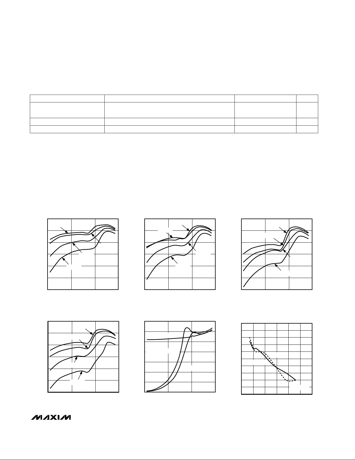
EFFICIENCY vs. LOAD CURRENT
(V
O
= 2.0V, f = 300kHz)
MAX1710-01
LOAD CURRENT (A)
EFFICIENCY (%)
VIN = 4.5V
VIN = 7V
VIN = 15V
VIN = 24V
40
60
50
80
70
90
100
0.01 0.1 1 10
EFFICIENCY vs. LOAD CURRENT
(V
O
= 1.6V, f = 300kHz)
MAX1710-02
LOAD CURRENT (A)
EFFICIENCY (%)
VIN = 4.5V
VIN = 24V
VIN = 7V
VIN = 15V
40
60
50
80
70
90
100
0.01 0.1 1 10
EFFICIENCY vs. LOAD CURRENT
(V
O
= 1.3V, f = 300kHz)
MAX1710-03
LOAD CURRENT (A)
EFFICIENCY (%)
VIN = 4.5V
VIN = 24V
VIN = 15V
VIN = 7V
40
60
50
80
70
90
100
0.01 0.1 1 10
EFFICIENCY vs. LOAD CURRENT
(V
O
= 1.6V, f = 550kHz)
MAX1710-04
LOAD CURRENT (A)
EFFICIENCY (%)
VIN = 4.5V
VIN = 15V
VIN = 7V
VIN = 24V
0
100
50
200
150
300
250
350
0.01 0.1 1 10
FREQUENCY vs. LOAD CURRENT
(V
O
= 1.6V)
MAX1710-05
LOAD CURRENT (A)
FREQUENCY (kHz)
VIN = 15V, PWM MODE
VIN = 4.5V, SKIP MODE
VIN = 15V, SKIP MODE
TON = OPEN
300
306
304
302
308
310
312
314
316
318
320
0 105 15 20 25 30
FREQUENCY vs. INPUT VOLTAGE
(I
O
= 7A)
MAX1710-06
INPUT VOLTAGE (V)
FREQUENCY (kHz)
VO = 2.0V
VO = 1.6V
TON = OPEN
Note 2: On-Time and Off-Time specifications are measured from 50% point to 50% point at the DH pin with LX forced to 0V, BST
forced to 5V, and a 250pF capacitor connected from DH to LX. Actual in-circuit times may differ due to MOSFET switching
speeds.
Note 3: Specifications from -40°C to 0°C are guaranteed but not production tested.
__________________________________________Typical Operating Characteristics
(7A CPU supply circuit of Figure 1, TA= +25°C, unless otherwise noted.)
CONDITIONS
Measured at FB with respect to unloaded output voltage,
falling edge, hysteresis = 1%
%-8.5 -2.5PGOOD Trip Threshold
I
SINK
= 1mA V0.4PGOOD Output Low Voltage
High state, forced to 5.5V µA1PGOOD Leakage Current
UNITMIN TYP MAXPARAMETER
ELECTRICAL CHARACTERISTICS (continued)
(Circuit of Figure 1, V
BATT
=15V, V
CC
= VDD= 5V, SKIP = GND, TA= -40°C to +85°C, unless otherwise noted.) (Note 3)
MAX1710/MAX1711
High-Speed, Digitally Adjusted
Step-Down Controllers for Notebook CPUs
6 _______________________________________________________________________________________
_____________________________Typical Operating Characteristics (continued)
(7A CPU supply circuit of Figure 1, TA= +25°C, unless otherwise noted.)
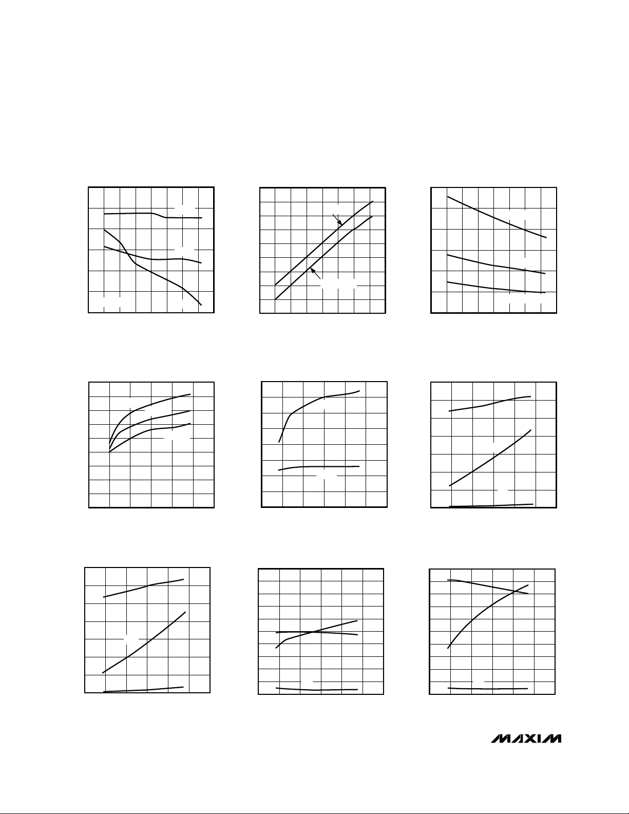
0
0.2
0.1
0.5
0.4
0.3
0.8
0.7
0.6
0.9
0 105 15 20 25 30
CONTINUOUS TO DISCONTINUOUS
INDUCTOR CURRENT POINT
vs. INPUT VOLTAGE
MAX1710-10
INPUT VOLTAGE (V)
LOAD CURRENT (A)
VO = 2.0V
VO = 1.6V
VO = 1.3V
10.0
10.5
11.0
11.5
12.0
12.5
13.0
13.5
14.0
0 105 15 20 25 30
INDUCTOR CURRENT PEAKS AND
VALLEYS vs. INPUT VOLTAGE
(AT CURRENT-LIMIT POINT)
MAX1710-11
INPUT VOLTAGE (V)
INDUCTOR CURRENT (A)
I
PEAK
I
VALLEY
0
0.2
0.1
0.4
0.3
0.6
0.5
0.7
0 5 15 2510 20 30
NO-LOAD SUPPLY CURRENTS
vs. INPUT VOLTAGE
(SKIP MODE, f = 300kHz)
MAX1710-12
INPUT VOLTAGE (V)
SUPPLY CURRENT (mA)
I
CC
I
BATT
I
DD
0
0.2
0.1
0.4
0.3
0.6
0.5
0.7
0 10 20 305 15 25
NO-LOAD SUPPLY CURRENTS
vs. INPUT VOLTAGE
(SKIP MODE, f = 550kHz)
MAX1710-13
INPUT VOLTAGE (V)
SUPPLY CURRENT (mA)
I
CC
I
BATT
I
DD
0
6
4
2
8
10
12
14
16
18
20
0 105 15 20 25 30
NO-LOAD SUPPLY CURRENTS
vs. INPUT VOLTAGE
(PWM MODE, f = 300kHz)
MAX1710-14
INPUT VOLTAGE (V)
SUPPLY CURRENT (mA)
I
DD
I
BAT
I
CC
0
6
4
2
8
10
12
14
16
18
20
0 105 15 20 25 30
NO-LOAD SUPPLY CURRENTS
vs. INPUT VOLTAGE
(PWM MODE, f = 550kHz)
MAX1710-15
INPUT VOLTAGE (V)
SUPPLY CURRENT (mA)
I
DD
I
BAT
I
CC
285
290
295
300
305
310
315
-60 -20-40 0 20 40 60 80 100
FREQUENCY vs. TEMPERATURE
(V
IN
= 15V, VO = 2.0V)
MAX1710-07
TEMPERATURE (°C)
FREQUENCY (kHz)
IO = 7A
IO = 4A
IO = 1A
TON = OPEN
456
460
458
466
464
462
472
470
468
474
-60 0 20-40 -20 40 60 80 100
ON-TIME vs. TEMPERATURE
MAX1710-08
TEMPERATURE (°C)
ON TIME (ns)
IO = 1A
IO = 4A OR 7A
0
5
10
15
20
25
30
-60 -20-40 0 20 40 60 80 100
CURRENT-LIMIT TRIP POINT
vs. TEMPERATURE
MAX1710-09
TEMPERATURE (°C)
CURRENT TRIP POINT (A)
I
LIM
= 400kΩ
I
LIM
= V
CC
I
LIM
= 100kΩ
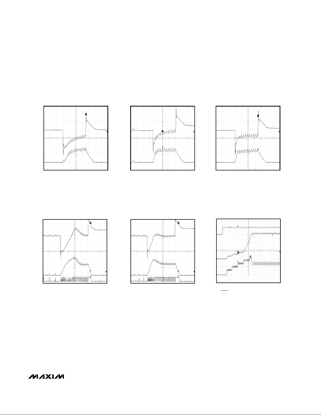
10µs/div
LOAD-TRANSIENT RESPONSE
(WITH INTEGRATOR)
VIN = 15V, VO = 1.6V, IO = 0A TO 7A
A = V
OUT
, AC COUPLED, 50mV/div
B = INDUCTOR CURRENT, 5A/div
A
B
MAX1710-16
10µs/div
LOAD-TRANSIENT RESPONSE
(WITH INTEGRATOR)
VIN = 15V, VO = 1.6V, IO = 30mA, TO 7A
A = V
OUT
, AC COUPLED, 50mV/div
B = INDUCTOR CURRENT, 5A/div
A
B
MAX1710-17
MAX1710/MAX1711
High-Speed, Digitally Adjusted
Step-Down Controllers for Notebook CPUs
_______________________________________________________________________________________ 7
_____________________________Typical Operating Characteristics (continued)
(7A CPU supply circuit of Figure 1, TA= +25°C, unless otherwise noted.)
20µs/div
LOAD-TRANSIENT RESPONSE
(WITH INTEGRATOR)
VIN = 4.5V, VO = 2V, IO = 30mA TO 7A
A = V
OUT
, AC COUPLED, 50mV/div
B = INDUCTOR CURRENT, 5A/div
C = DL, 10V/div
A
B
C
MAX1710-19
20µs/div
LOAD-TRANSIENT RESPONSE
(WITH INTEGRATOR)
VIN = 4.5V, VO = 1.3V, IO = 30mA TO 7A
A = V
OUT
, AC COUPLED, 50mV/div
B = INDUCTOR CURRENT, 5A/div
C = DL, 10V/div
A
B
C
MAX1710-20
500µs/div
START-UP WAVEFORM
A = SHDN
B = V
OUT
, 0.5V/div
C = INDUCTOR CURRENT, 5A/div
A
B
C
MAX1710-21
10µs/div
LOAD-TRANSIENT RESPONSE
(WITHOUT INTEGRATOR)
VIN = 15V, VO = 1.6V, IO = 30mA TO 7A
A = V
OUT
, AC COUPLED, 50mV/div
B = INDUCTOR CURRENT, 5A/div
A
B
MAX1710-18
MAX1710/MAX1711
High-Speed, Digitally Adjusted
Step-Down Controllers for Notebook CPUs
8 _______________________________________________________________________________________
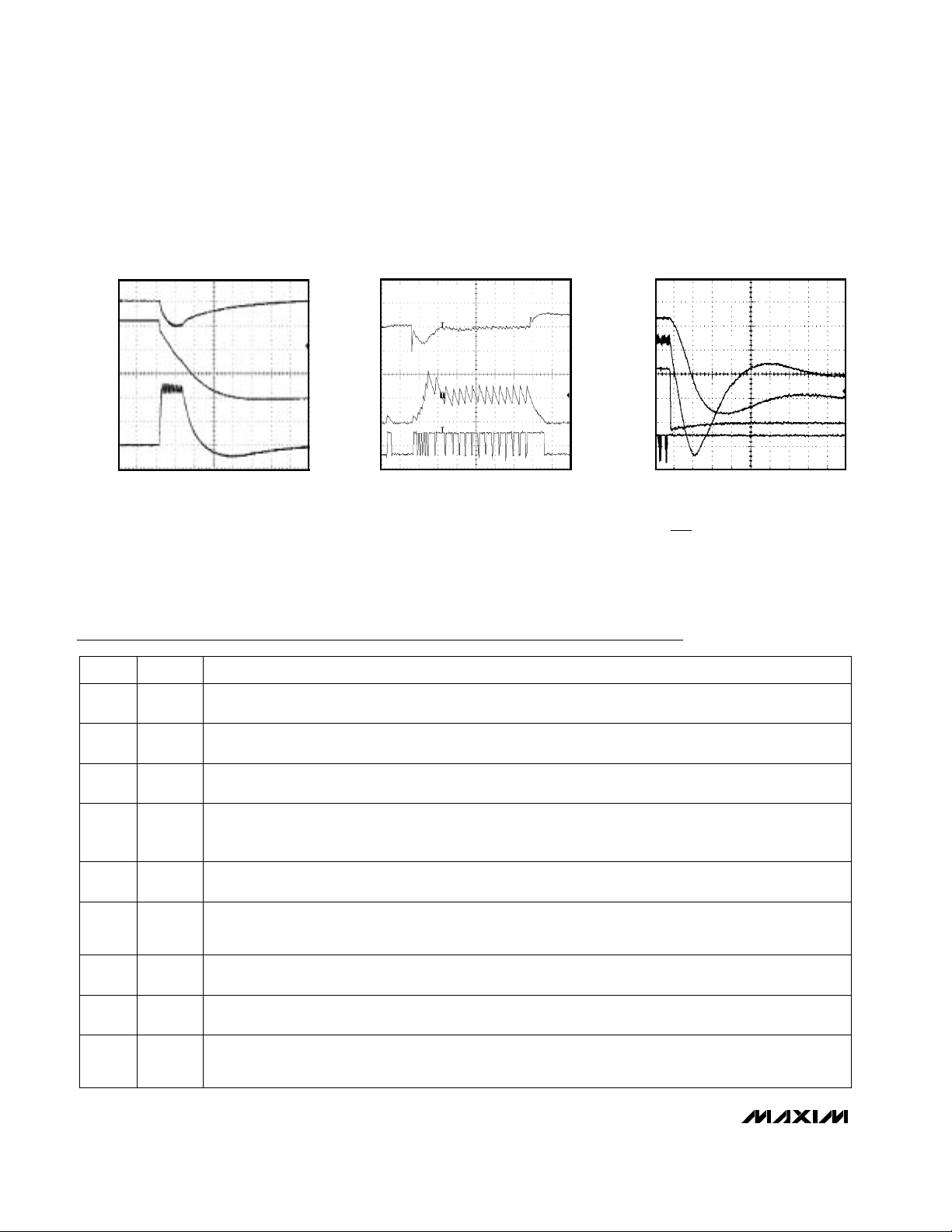
50µs/div
OUTPUT OVERLOAD WAVEFORM
V
OUT
= 1.6V
A = V
IN
, AC COUPLED, 2V/div
B = V
OUT
, 0.5V/div
C = INDUCTOR CURRENT, 5A/div
A
B
C
MAX1710-22
5µs/div
LOAD-TRANSIENT RESPONSE
L = 0.7µH, V
OUT
= 1.6V, VIN = 15V, C
OUT
= 47µF (x4), f = 550kHz
A = V
OUT
, AC COUPLED, 100mV/div
B = INDUCTOR CURRENT, 5A/div
C = DL, 5V/div
A
B
C
MAX1710-23
CERAMIC C
OUT
5µs/div
SHUTDOWN WAVEFORM
VIN = 15V, V0 = 1.6V, I0 = 7A
A = V
OUT
, 0.5V/div
B = INDUCTOR CURRENT, 5A/div
C = SHDN, 2V/div
D = DL, 5V/div
A
B
C
D
MAX1710-24
_____________________________Typical Operating Characteristics (continued)
(7A CPU supply circuit of Figure 1, TA= +25°C, unless otherwise noted.)
Pin Description
NAME FUNCTION
5 CC
Integrator Capacitor Connection. Connect a 100pF to 1000pF (470pF typical) capacitor to GND to set the
integration time constant.
PIN
4 FBS
Feedback Remote-Sense Input, normally connected to V
OUT
directly at the load. FBS internally connects to
the integrator that fine-tunes the DC output voltage. Tie FBS to VCCto disable all three integrator amplifiers.
Tie FBS to FB (or disable the integrators) when externally adjusting the output voltage with a resistor-divider.
3 FB
Fast Feedback Input, normally connected to V
OUT
. FB is connected to the bulk output filter capacitors local-
ly at the power supply. An external resistor-divider can optionally set the output voltage.
8 TON
On-Time Selection Control Input. This is a four-level input that sets the K factor to determine DH on-time.
GND = 550kHz, REF = 400kHz, open = 300kHz, V
CC
= 200kHz.
7 V
CC
Analog Supply Voltage Input for PWM Core, 4.5V to 5.5V. Bypass VCCto GND with a 0.1µF minimum
capacitor.
6 ILIM
Current-Limit Threshold Adjustment. Connects to an external resistor to GND. The LX-PGND current-limit
threshold defaults to +100mV if ILIM is tied to VCC. The current-limit threshold is 1/10 of the voltage forced at
ILIM. In adjustable mode the threshold is V
TH
= R
LIM
· 5µA/10.
1 CC
Battery Voltage Sense Connection. V+ is used only for PWM one-shot timing. DH on-time is inversely proportional to V+ input voltage over a range of 2V to 28V.
9 REF
2.0V Reference Output. Bypass REF to GND with a 0.22µF minimum capacitor. REF can source 50µA for
external loads. Loading REF degrades FB accuracy according to the REF load-regulation error
(see
Electrical Characteristics
).
2
SHDN
Shutdown Control Input, active low. SHDN cannot withstand the battery voltage. In shutdown mode, DL is
forced to V
DD
in order to enforce overvoltage protection, even when powered down (unless OVP is high).
MAX1710/MAX1711
High-Speed, Digitally Adjusted
Step-Down Controllers for Notebook CPUs
_______________________________________________________________________________________ 9
Standard Application Circuit
The standard application circuit (Figure 1) generates a
low-voltage, high-power rail for supplying up to 7A to the
core CPU VCCin a notebook computer. This DC-DC
converter steps down a battery or AC adapter voltage to
sub-2V levels with high efficiency and accuracy, and
represents a good compromise between size, efficiency,
and cost.
See the MAX1710 EV kit manual for a list of components
and suppliers.
Detailed Description
The MAX1710/MAX1711 buck controllers are targeted
for low-voltage, high-current CPU power supplies for
notebook computers. CPU cores typically exhibit 0 to
10A or greater load steps when the clock is throttled.
The proprietary QUICK-PWM pulse-width modulator in
the MAX1710/MAX1711 is specifically designed for handling these fast load steps while maintaining a relatively
constant operating frequency and inductor operating
point over a wide range of input voltages. The QUICKPWM architecture circumvents the poor load-transient
timing problems of fixed-frequency current-mode PWMs
Pin Description (continued)
NAME FUNCTION
16
(MAX1711)
D4 DAC Code Input, MSB, 5µA internal pull-up to VCC(Tables 1 and 2).
PIN
13 DL Low-Side Gate-Driver Output, swings 0 to VDD.
12 PGOOD Open-Drain Power-Good Output.
11 GNDS
Ground Remote-Sense Input, normally connected to ground directly at the load. GNDS internally connects to the integrator that fine-tunes the ground offset voltage.
10 GND Analog Ground
14 PGND Power Ground. Also used as the inverting input for the current-limit comparator.
15 V
DD
Supply Voltage Input for the DL gate driver, 4.5V to 5.5V
17 D3 DAC Code Input. 5µA internal pull-up to VCC.
16
(MAX1710)
OVP
Overvoltage-Protection Disable Control Input (Table 3). GND = normal operation and overvoltage
protection active, V
CC
= overvoltage protection disabled.
22 BST
Boost Flying-Capacitor Connection. An optional resistor in series with BST allows the DH pull-up
current to be adjusted (Figure 5). This technique of slowing the LX rise time can be used to prevent
accidental turn-on of the low-side MOSFET due to excessive gate-drain capacitance.
21
SKIP
Low-Noise-Mode Selection Control Input. Low-noise forced-PWM mode causes inductor current
recirculation at light loads and suppresses pulse-skipping operation. Normal operation prevents
current recirculation. SKIP can also be used to disable both overvoltage and undervoltage protection
circuits and clear the fault latch (Figure 6). GND = normal operation, V
CC
= low-noise mode. Do not
leave
SKIP floating.
20 D0 DAC Code Input LSB. 5µA internal pull-up.
19 D1 DAC Code Input. 5µA internal pull-up.
18 D2 DAC Code Input. 5µA internal pull-up.
24 DH High-Side Gate-Driver Output. Swings LX to BST.
23 LX
Inductor Connection. LX serves as the lower supply rail for the DH high-side gate driver. Also used
for the noninverting input to the current-limit comparator as well as the skip-mode zero-crossing comparator.

MAX1710/MAX1711
while also avoiding the problems caused by widely varying switching frequencies in conventional constant-ontime and constant-off-time PWM schemes.
+5V Bias Supply (VCCand VDD)
The MAX1710/MAX1711 requires an external +5V bias
supply in addition to the battery. Typically, this +5V bias
supply is the notebook’s 95% efficient 5V system supply.
Keeping the bias supply external to the IC improves efficiency and eliminates the cost associated with the +5V
linear regulator that would otherwise be needed to supply the PWM circuit and gate drivers. If stand-alone
capability is needed, the +5V supply can be generated
with an external linear regulator such as the MAX1615.
The battery and +5V bias inputs can be tied together if
the input source is a fixed 4.5V to 5.5V supply. If the +5V
bias supply is powered up prior to the battery supply, the
enable signal (SHDN) must be delayed until the battery
voltage is present in order to ensure start-up. The +5V
bias supply must provide V
CC
and gate-drive power, so
the maximum current drawn is:
I
BIAS
= ICC+ f · (QG1+ QG2) = 15mA to 30mA (typ)
High-Speed, Digitally Adjusted
Step-Down Controllers for Notebook CPUs
10 ______________________________________________________________________________________
V
CC
V
BATT
4.5V TO 28V
+5V
BIAS SUPPLY
C2
3 x 470µF
KEMET T510
PANASONIC
ETQP6F2R0HFA
POWER-GOOD
INDICATOR
* MAX1710 ONLY
** MAX1711 ONLY
L1
2µH
V
OUT
1.25V TO 2V AT 7A (MAX1710)
0.925V TO 2V AT 7A (MAX1711)
SHDN
V+
221
2
21
20
19
18
17
24
23
13
14
3
4
11
R4
1k
12
7
15
D2
CMPSH-3
C6
1µF
C7
0.1µF
C4
1µF
C3
470pF
TO V
CC
Q1
D1
R2
100k
D3
(OPTIONAL OVP
REVERSE-POLARITY
CLAMP)
Q2
C5
1µF
R1
20Ω
C1 3 x 10µF/30V
SKIP
D0
D1
D2
DAC
INPUTS
ON/OFF
CONTROL
LOW-NOISE
CONTROL
DL
LX
BST
DH
PGND
FB
FBS
GNDS
Q1 = IRF7807
Q2 = IRF7805
D1, D3 = MBRS130T3 (OPTIONAL)
C1 = Sanyo OS-CON (30SC10M)
PGOOD
V
DD
MAX1710
MAX1711
8
9
5
6
16
+5V
10
D3
16
D4**
TON
REF
CC
GND
R3
(OPTIONAL)
ILIM OVP*
Figure 1. Standard Application Circuit

where ICCis 600µA typical, f is the switching frequency,
and QG1and QG2are the MOSFET data sheet total
gate-charge specification limits at VGS= 5V.
Free-Running, Constant-On-Time PWM
Controller with Input Feed-Forward
The QUICK-PWM control architecture is an almost fixedfrequency, constant-on-time current-mode type with voltage feed-forward (Figure 2). This architecture relies on
the filter capacitor’s ESR to act as the current-sense
resistor, so the output ripple voltage provides the PWM
ramp signal. The control algorithm is simple: the highside switch on-time is determined solely by a one-shot
whose period is inversely proportional to input voltage
and directly proportional to output voltage. Another oneshot sets a minimum off-time (400ns typical). The on-time
one-shot is triggered if the error comparator is low, the
MAX1710/MAX1711
High-Speed, Digitally Adjusted
Step-Down Controllers for Notebook CPUs
______________________________________________________________________________________ 11
REF
-5%
FROM
D/A
REF
REF
D0 D1 D2 D3
10k
ERROR
AMP
TOFF
TON
REF
+12%
FB
REF
-30%
R-2R
D/A CONVERTER
CHIP SUPPLY
g
m
g
m
g
m
GNDS
CC
SHDN
FBS
PGOOD
OVP/UVLO
LATCH
ON-TIME
COMPUTE
TON
1-SHOT
1-SHOT
TRIG
V
BATT
2V TO 28V
TRIG
Q
Q
S
R
2V
REF
GND
REF
FB
PGND
+5V
OUTPUT
DL
V
CC
V
CC
V
DD
LX
ZERO CROSSING
CURRENT
LIMIT
DH
BST
I
LIM
R
LIM
+5V
5µA
+5V
Q
S1
Q
S2 TIMER
SKIP
OVP
TON
V+
70k
Σ
MAX1710
S
R
Q
Figure 2. MAX1710 Functional Diagram

MAX1710/MAX1711
High-Speed, Digitally Adjusted
Step-Down Controllers for Notebook CPUs
12 ______________________________________________________________________________________
low-side switch current is below the current-limit threshold, and the minimum off-time one-shot has timed out.
On-Time One-Shot (TON)
The heart of the PWM core is the one-shot that sets the
high-side switch on-time. This fast, low-jitter, adjustable
one-shot includes circuitry that varies the on-time in
response to battery and output voltage. The high-side
switch on-time is inversely proportional to the battery
voltage as measured by the V+ input, and directly proportional to the output voltage as set by the DAC code.
This algorithm results in a nearly constant switching frequency despite the lack of a fixed-frequency clock generator. The benefits of a constant switching frequency
are twofold: first, the frequency can be selected to avoid
noise-sensitive regions such as the 455kHz IF band;
second, the inductor ripple-current operating point
remains relatively constant, resulting in easy design
methodology and predictable output voltage ripple.
On-Time = K (V
OUT
+ 0.075V) / V
IN
where K is set by the TON pin-strap connection and
0.075V is an approximation to accommodate for the
expected drop across the low-side MOSFET switch.
One-shot timing error increases for the shorter on-time
settings due to fixed propagation delays and is approximately ±12.5% at 550kHz and 400kHz, and ±10% at the
two slower settings. This translates to reduced switching-frequency accuracy at higher frequencies. (see
Table 5). Switching frequency increases as a function of
load current due to the increasing drop across the low-
Table 1. MAX1710 FB Output Voltage
DAC Codes
D3 D2 D1 D0
OUTPUT
VOLTAGE (V)
1 0 0 0 1.60
0 0 0 0 2.00
0 0 0 1 1.95
0 0 1 0 1.90
0 0 1 1 1.85
0 1 0 0 1.80
0 1 0 1 1.75
0 1 1 0 1.70
0 1 1 1 1.65
1 0 0 1 1.55
1 0 1 0 1.50
1 0 1 1 1.45
1 1 0 0 1.40
1 1 0 1 1.35
1 1 1 0 1.30
1 1 1 1 1.25
Table 2. MAX1711 FB Output Voltage
DAC Codes
D4 D3 D2 D1
OUTPUT
VOLTAGE (V)
0 1 0 0 1.60
0 0 0 0 2.00
0 0 0 0 1.95
0 0 0 1 1.90
0 0 0 1 1.85
0 0 1 0 1.80
0 0 1 0 1.75
0 0 1 1 1.70
0 0 1 1 1.65
0 1 0 0 1.55
0 1 0 1 1.50
0 1 0 1 1.45
0 1 1 0 1.40
0 1 1 0 1.35
0 1 1 1 1.30
0 1 1 1 Shutdown 3*
1 1 0 0 1.075
1 0 0 0 1.275
1 0 0 0 1.250
1 0 0 1 1.225
1 0 0 1 1.200
1 0 1 0 1.175
1 0 1 0 1.150
1 0 1 1 1.125
1 0 1 1 1.100
1 1 0 0 1.050
1 1 0 1 1.025
1 1 0 1 1.000
1 1 1 0 0.975
1 1 1 0 0.950
1 1 1 1 0.925
1 1 1 1 Shutdown 3*
D0
0
0
1
0
1
0
1
0
1
1
0
1
0
1
0
1
0
0
1
0
1
0
1
0
1
1
0
1
0
1
0
1
* See Table 3

MAX1710/MAX1711
High-Speed, Digitally Adjusted
Step-Down Controllers for Notebook CPUs
______________________________________________________________________________________ 13
side MOSFET, which causes a faster inductor-current
discharge ramp. The on-times guaranteed in the
Electrical Characteristics
are influenced by switching
delays in the external high-side power MOSFET. The
exact switching frequency will depend on gate charge,
internal gate resistance, source inductance, and DH output drive characteristics.
Two external factors that can influence switching-frequency accuracy are resistive drops in the two conduction loops (including inductor and PC board resistance)
and the dead-time effect. These effects are the largest
contributors to the change of frequency with changing
load current. The dead-time effect is a notable discontinuity in the switching frequency as the load current is
varied (see
Typical Operating Characteristics
). It occurs
whenever the inductor current reverses, most commonly
at light loads with SKIP high. With reversed inductor current, the inductor’s EMF causes LX to go high earlier
than normal, extending the on-time by a period equal to
the low-to-high dead time. For loads above the critical
conduction point, the actual switching frequency is:
where V
DROP1
is the sum of the parasitic voltage drops
in the inductor discharge path, including synchronous
rectifier, inductor, and PC board resistances; V
DROP2
is
the sum of the resistances in the charging path, and t
ON
is the on-time calculated by the MAX1710/MAX1711.
Integrator Amplifiers (CC)
There are three integrator amplifiers that provide a fine
adjustment to the output regulation point. One amplifier
monitors the difference between GNDS and GND, while
another monitors the difference between FBS and FB.
The third amplifier integrates the difference between REF
and the DAC output. These three transconductance
amplifiers’ outputs are directly summed inside the chip,
so the integration time constant can be set easily with a
capacitor. The gmof each amplifier is 160µmho (typical).
The integrator block has an ability to move and correct
the output voltage by about -2%, +4%. For each amplifier, the differential input voltage range is about ±50mV
total, including DC offset and AC ripple. The voltage
gain of each integrator is about 80V/V.
The FBS amplifier corrects for DC voltage drops in PC
board traces and connectors in the output bus path
between the DC-DC converter and the load. The GNDS
amplifier performs a similar DC correction task for the
output ground bus. The third amplifier provides an averaging function that forces V
OUT
to be regulated at the
average value of the output ripple waveform. If the integrator amplifiers are disabled, V
OUT
is regulated at the
valleys of the output ripple waveform. This creates a
slight load-regulation characteristic in which the output
voltage rises approximately 1% (up to 1/2 the peak
amplitude of the ripple waveform as a limit) when under
light loads.
Integrators have both beneficial and detrimental characteristics. While they do correct for drops due to DC bus
resistance and tighten the DC output voltage tolerance
limits by averaging the peak-to-peak output
ripple, they can interfere with achieving the fastest possible load-transient response. The fastest transient
response is achieved when all three integrators are disabled. This works very well when the MAX1710/
MAX1711 circuit can be placed very close to the CPU.
There is often a connector, or at least many milliohms of
PC board trace resistance, between the DC-DC converter and the CPU. In these cases, the best strategy is to
place most of the bulk bypass capacitors close to the
CPU, with just one capacitor on the other side of the
connector near the MAX1710/MAX1711 to control ripple
if the CPU card is unplugged. In this situation, the
remote-sense lines and integrators provide a real benefit.
When both GNDS and FBS are tied to VCCso that all
three integrators are disabled, CC can be left unconnected, which eliminates a component.
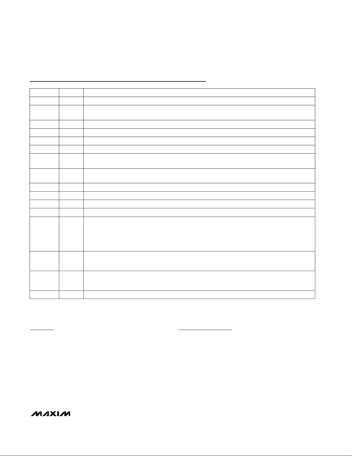
Automatic Pulse-Skipping Switchover
At light loads, an inherent automatic switchover to PFM
takes place. This switchover is effected by a comparator
that truncates the low-side switch on-time at the inductor
current’s zero crossing. This mechanism causes the
threshold between pulse-skipping PFM and non-skipping PWM operation to coincide with the boundary
between continuous and discontinuous inductor-current
operation (also known as the “critical conduction” point;
see Continuous to Discontinuous Inductor Current Point
vs. Input Voltage graphs in the
Typical Operating
Characteristics
). For a battery range of 7V to 24V this
threshold is relatively constant, with only a minor dependence on battery voltage.
where K is the On-Time Scale factor (see Table 5). The
load-current level at which PFM/PWM crossover occurs,
I
LOAD(SKIP)
, is equal to 1/2 the peak-to-peak ripple current, which is a function of the inductor value (Figure 3).
For example, in the standard application circuit with t
ON
= 300ns at 24V, V
OUT
= 2V, and L = 2µH, switchover to
pulse-skipping operation occurs at I
LOAD
= 1.65A or
I
K
L
LOAD SKIP
( )
≈
2
f
V V
t V V
OUT DROP
ON IN DROP
=
+
+
( )
1
2
MAX1710/MAX1711
High-Speed, Digitally Adjusted
Step-Down Controllers for Notebook CPUs
14 ______________________________________________________________________________________
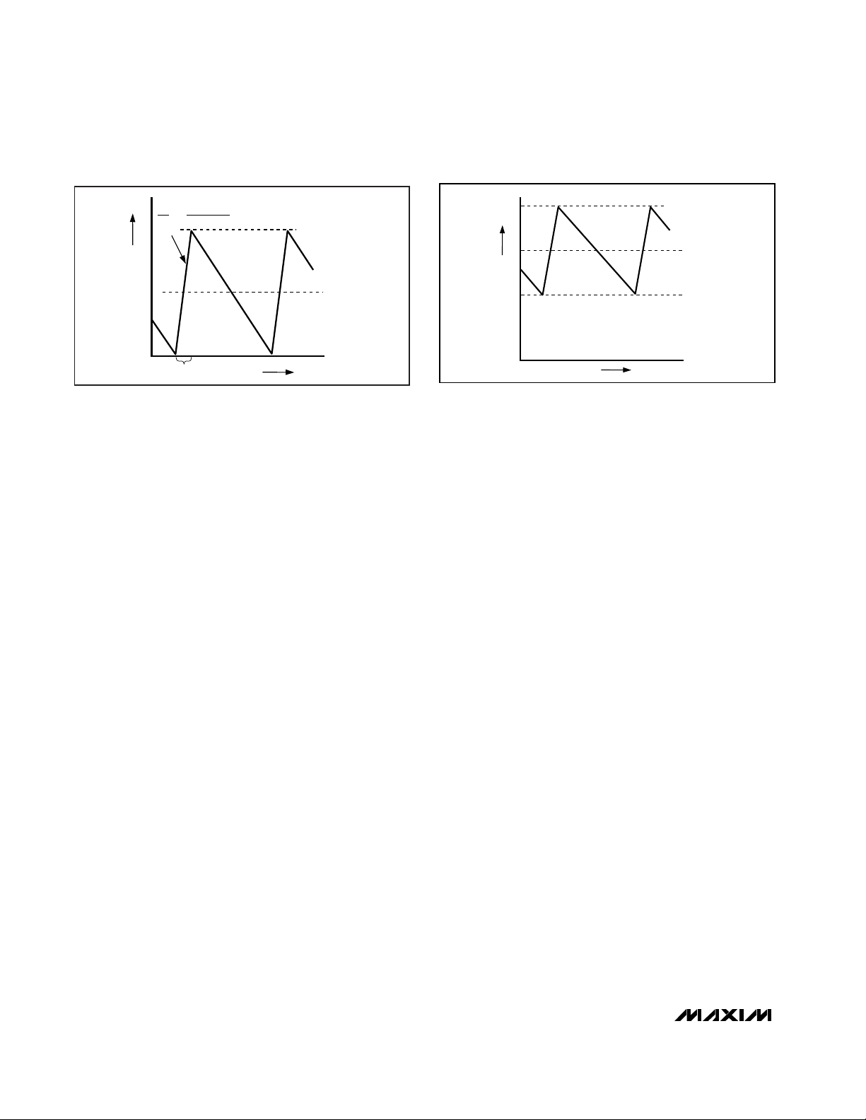
Figure 4. ‘‘Valley’’ Current-Limit Threshold Point
INDUCTOR CURRENT
I
LIMIT
I
LOAD
0 TIME
LX-PGND I
LIMIT
THRESHOLD = 100mV (NOMINAL, DEFAULT)
VOLTAGE DROP ACROSS Q2
-I
PEAK
about 1/4 full load. The crossover point occurs at an
even lower value if a swinging (soft-saturation) inductor
is used.
The switching waveforms may appear noisy and asynchronous when light loading causes pulse-skipping
operation, but this is a normal operating condition that
results in high light-load efficiency. Trade-offs in PFM
noise vs. light-load efficiency can be made by varying
the inductor value. Generally, low inductor values produce a broader efficiency vs. load curve, while higher
values result in higher full-load efficiency (assuming that
the coil resistance remains fixed) and less output voltage
ripple. Penalties for using higher inductor values include
larger physical size and degraded load-transient
response (especially at low input voltage levels).
Forced-PWM Mode (
SSKKIIPP
= High)
The low-noise, forced-PWM mode (SKIP driven high) disables the zero-crossing comparator, which controls the
low-side switch on-time. This causes the low-side gatedrive waveform to become the complement of the highside gate-drive waveform. This in turn causes the
inductor current to reverse at light loads, as the PWM
loop strives to maintain a duty ratio of V
OUT/VIN
. The
benefit of forced-PWM mode is to keep the switching frequency fairly constant, but it comes at a cost: the noload battery current can be as high as 40mA or more.
Forced-PWM mode is most useful for reducing audio-frequency noise, improving load-transient response, providing sink-current capability for dynamic output voltage
adjustment, and improving the cross-regulation of multiple-output applications that use a flyback transformer or
coupled inductor.
Current-Limit Circuit (ILIM)
The current-limit circuit employs a unique “valley” current-sensing algorithm that uses the on-state resistance
of the low-side MOSFET as a current-sensing element. If
the current-sense signal is above the current-limit
threshold, the PWM is not allowed to initiate a new cycle
(Figure 4). The actual peak current is greater than the
current-limit threshold by an amount equal to the inductor ripple current. Therefore the exact current-limit characteristic and maximum load capability are a function of
the MOSFET on-resistance, inductor value, and battery
voltage. The reward for this uncertainty is robust, lossless overcurrent sensing. When combined with the UVP
protection circuit, this current-limit method is effective in
almost every circumstance.
There is also a negative current limit that prevents excessive reverse inductor currents when V
OUT
is sinking current. The negative current-limit threshold is set to
approximately 120% of the positive current limit, and
therefore tracks the positive current limit when ILIM is
adjusted.
The current-limit threshold can be adjusted with an external resistor (R
LIM
) at ILIM. A precision 5µA pull-up current source at ILIM sets a voltage drop on this resistor,
adjusting the current-limit threshold from 50mV to
200mV. In the adjustable mode, the current-limit threshold voltage is precisely 1/10th the voltage seen at ILIM.
Therefore, choose R
LIM
equal to 2kΩ/mV of the currentlimit threshold. The threshold defaults to 100mV when
ILIM is tied to VCC. The logic threshold for switchover to
the 100mV default value is approximately VCC- 1V.
The adjustable current limit can accommodate
MOSFETs with atypical on-resistance characteristics
(see
Design Procedure
).
A capacitor in parallel with R
LIM
can provide a variable
soft-start function.
Carefully observe the PC board layout guidelines to
ensure that noise and DC errors don’t corrupt the current-sense signals seen by LX and PGND. The IC must
be mounted close to the low-side MOSFET with short,
Figure 3. Pulse-Skipping/Discontinuous Crossover Point
INDUCTOR CURRENT
I
LOAD
= I
PEAK
/2
ON-TIME0 TIME
-I
PEAK
L
V
BATT -VOUT
∆i
∆t
=

MAX1710/MAX1711
High-Speed, Digitally Adjusted
Step-Down Controllers for Notebook CPUs
______________________________________________________________________________________ 15
direct traces making a Kelvin sense connection to the
source and drain terminals.
MOSFET Gate Drivers (DH, DL)
The DH and DL drivers are optimized for driving moderate-size, high-side and larger, low-side power MOSFETs.
This is consistent with the low duty factor seen in the
notebook CPU environment, where a large V
BATT
- V
OUT
differential exists. An adaptive dead-time circuit monitors
the DL output and prevents the high-side FET from turning on until DL is fully off. There must be a low-resistance, low-inductance path from the DL driver to the
MOSFET gate in order for the adaptive dead-time circuit
to work properly. Otherwise, the sense circuitry in the
MAX1710/MAX1711 will interpret the MOSFET gate as
“off” while there is actually still charge left on the gate.
Use very short, wide traces measuring 10 to 20 squares
(50 to 100 mils wide if the MOSFET is 1 inch from the
MAX1710/MAX1711).
The dead time at the other edge (DH turning off) is determined by a fixed 35ns (typical) internal delay.
The internal pull-down transistor that drives DL low is
robust, with a 0.5Ω typical on-resistance. This helps prevent DL from being pulled up during the fast rise-time of
the inductor node, due to capacitive coupling from the
drain to the gate of the massive low-side synchronousrectifier MOSFET. However, you might still encounter
some combinations of high- and low-side FETs that will
cause excessive gate-drain coupling, which can lead to
efficiency-killing, EMI-producing shoot-through currents.
This can often be remedied by adding a resistor in series
with BST, which increases the turn-on time of the highside FET without degrading the turn-off time.
DAC Converter (D0–D4)
The digital-to-analog converter (DAC) programs the output voltage. It receives a digital code from pins on the
CPU module that are either hard-wired to GND or left
open-circuit. Note that the codes don’t match any desktop VRM codes. The MAX1710/MAX1711 contain weak
internal pull-ups on each input in order to eliminate external resistors.
When changing MAX1710 DAC codes while powered
up, the over/undervoltage protection features can be
activated if the code is changed more than 1LSB at a
time. For applications needing the capability of changing
DAC codes “on-the-fly,” use the MAX1711.
POR, UVLO, and Soft-Start
Power-on reset (POR) occurs when VCCrises above
approximately 2V, resetting the fault latch and soft-start
counter, and preparing the PWM for operation. V
CC
undervoltage lockout (UVLO) circuitry inhibits switching
and forces the DL gate driver high (in order to enforce
output overvoltage protection) until V
CC
rises above
4.2V, whereupon an internal digital soft-start timer begins
to ramp up the maximum allowed current limit. The ramp
occurs in five steps: 20%, 40%, 60%, 80%, and 100%,
with 100% current available after 1.7ms ±50%.
A continuously adjustable, analog soft-start function can
be realized by adding a capacitor in parallel with R
LIM
at
ILIM. This soft-start method requires a minimum interval
between power-down and power-up to allow R
LIM
to dis-
charge the capacitor.
Power-Good Output (PGOOD)
The output (FB) is continuously monitored for undervoltage by the PGOOD comparator, except in shutdown or
standby mode. The -5% undervoltage trip threshold is
measured with respect to the nominal unloaded output
voltage, as set by the DAC. If the DAC code increases in
steps greater than 1LSB, it is likely that PGOOD will
momentarily go low. In shutdown and standby modes,
PGOOD is actively held low. The PGOOD output is a true
open-drain type with no parasitic ESD diodes. Note that
the PGOOD undervoltage detector is completely independent of the output UVP fault detector.
Output Overvoltage Protection (OVP)
The overvoltage protection circuit is designed to protect
against a shorted high-side MOSFET by drawing high
current and blowing the battery fuse. The FB node is
continuously monitored for overvoltage. The overvoltage
trip threshold tracks the DAC code setting. If the output
is more than 12.5% above the nominal regulation point
for the MAX1710 (2.25V absolute for the MAX1711),
overvoltage protection (OVP) is triggered and the circuit
shuts down. The DL low-side gate-driver output is then
latched high until SHDN is toggled or VCCpower is
cycled below 1V. This action turns on the synchronousrectifier MOSFET with 100% duty and, in turn, rapidly discharges the output filter capacitor and forces the output
to ground.
If the condition that caused the overvoltage (such as a
shorted high-side MOSFET) persists, the battery fuse will
blow. Note that DL going high can have the effect of
causing output polarity reversal, due to energy stored in
the output LC at the instant OVP activates. If the load
can’t tolerate being forced to a negative voltage, it may
be desirable to place a power Schottky diode across the
output to act as a reverse-polarity clamp (Figure 1). The
MAX1710/MAX1711 itself can be affected by the FB pin
going below ground, with the negative voltage coupling
into SHDN. It may be necessary to add 1kΩ resistors in
series with FB and FBS (Figure 7).

MAX1710/MAX1711
High-Speed, Digitally Adjusted
Step-Down Controllers for Notebook CPUs
16 ______________________________________________________________________________________
DL is also kept high continuously when VCCUVLO is
active as well as in Shutdown1 mode (Table 3).
Overvoltage protection can be defeated via the OVP
input (MAX1710 only) or via a SKIP test mode (see
Pin
Description
).
Output Undervoltage Protection (UVP)
The output undervoltage protection function is similar to
foldback current limiting, but employs a timer rather than
a variable current limit. If the MAX1710 output (FB) is
under 70% of the nominal value 20ms after coming out of
shutdown, the PWM is latched off and won’t restart until
V
CC
power is cycled or SHDN is toggled. For the
MAX1711, the nominal UVP trip threshold is fixed at 0.8V.
No-Fault Test Mode
The over/undervoltage protection features can complicate the process of debugging prototype breadboards,
since there are (at most) a few milliseconds in which to
determine what went wrong. Therefore, a test mode is
provided to totally disable the OVP, UVP, and thermal
shutdown features, and clear to the fault latch if it has
been previously set. The PWM operates as if SKIP were
grounded (PFM/PWM mode).
The no-fault test mode is entered by sinking 1.5mA
from SKIP via an external negative voltage source in
series with a resistor (Figure 6). SKIP is clamped to
GND with a silicon diode, so choose the resistor value
equal to (V
FORCE
- 0.65V) / 1.5mA.
Design Procedure
Firmly establish the input voltage range and maximum
load current before choosing a switching frequency and
inductor operating point (ripple current ratio). The prima-
SHDN SKIP OVP
DL MODE COMMENTS
1 X
0 X 0 High Shutdown1 Low-power shutdown state. DL is forced to VDD, enforcing OVP. ICC< 1µA typ.
X Low
0 X 1 Low Shutdown2
Low-power shutdown state. DL is forced to GND, disabling OVP. ICC< 1µA typ.
Exiting shutdown triggers a soft-start cycle.
Shutdown3
(MAX1711
only)
DAC code = X1111 (see Table 2) DL is forced to PGND, DH is forced to LX. The
MAX1711 eventually goes into UVP fault mode as the load current discharges the
output.
1
Below
GND
X Switching No Fault
Test mode with OVP, UVP, and thermal faults disabled and latches cleared.
Otherwise normal operation, with automatic PWM/PFM switchover for pulse
skipping at light loads (Figure 6).
1 X 1 Switching No OVP
OVP faults disabled and OVP latch cleared. Otherwise normal operation,
with SKIP controlling PWM/PFM switchover.
1 V
CC
X Switching
Run (PWM),
Low Noise
Low-noise operation with no automatic switchover. Fixed-frequency PWM action
is forced regardless of load. Inductor current reverses at light load levels.
ICCdraw = 750µA typ. IDDdraw = 15mA typ.
1 GND X Switching
Run
(PFM/PWM)
Normal operation with automatic PWM/PFM switchover for pulse skipping at light
loads. ICC= 600µA typ. IDDdraw = load dependent.
1 X X High Fault
Fault latch has been set by OVP, output UVLO, or thermal shutdown. Device will
remain in FAULT mode until V
CC
power is cycled, SKIP is forced below ground,
or SHDN is toggled.
Table 3. Operating Mode Truth Table
Good operating point for
compound buck designs
or desktop circuits.
+5V-input notebook
CPU core
550
400
3-cell Li+ notebook
CPU core
Useful in 4-cell systems
for lighter loads than the
CPU or where size is key.
Considered mainstream
by current standards.
4-cell Li+ notebook
CPU core
300
200
4-cell Li+ notebook
CPU core
Use for absolute best
efficiency.
COMMENT
TYPICAL
APPLICATION
FREQUENCY
(kHz)
Table 4. Frequency Selection Guidelines

MAX1710/MAX1711
______________________________________________________________________________________ 17
High-Speed, Digitally Adjusted
Step-Down Controllers for Notebook CPUs
ry design trade-off lies in choosing a good switching frequency and inductor operating point, and the following
four factors dictate the rest of the design:
1) Input voltage range. The maximum value
(V
BATT(MAX)
) must accommodate the worst-case high
AC adapter voltage. The minimum value (V
BATT(MIN)
)
must account for the lowest battery voltage after
drops due to connectors, fuses, and battery selector
switches. If there is a choice at all, lower input voltages result in better efficiency.
2) Maximum load current. There are two values to con-
sider. The
peak load current
(I
LOAD(MAX)
) determines
the instantaneous component stresses and filtering
requirements, and thus drives output capacitor
selection, inductor saturation rating, and the design
of the current-limit circuit. The
continuous load cur-
rent
(I
LOAD
) determines the thermal stresses and
thus drives the selection of input capacitors,
MOSFETs, and other critical heat-contributing components. Modern notebook CPUs generally exhibit
I
LOAD
= I
LOAD(MAX)
· 80%.
3) Switching frequency. This choice determines the
basic trade-off between size and efficiency. The optimal frequency is largely a function of maximum input
voltage, due to MOSFET switching losses that are
proportional to frequency and VBATT2. The optimum
frequency is also a moving target, due to rapid
improvements in MOSFET technology that are making
higher frequencies more practical (Table 4).
4) Inductor operating point. This choice provides
trade-offs between size vs. efficiency. Low inductor
values cause large ripple currents, resulting in the
smallest size, but poor efficiency and high output
noise. The minimum practical inductor value is one
that causes the circuit to operate at the edge of critical conduction (where the inductor current just touch-
es zero with every cycle at maximum load). Inductor
values lower than this grant no further size-reduction
benefit.
The MAX1710/MAX1711’s pulse-skipping algorithm
initiates skip mode at the critical-conduction point. So,
the inductor operating point also determines the loadcurrent value at which PFM/PWM switchover occurs.
The optimum point is usually found between 20% and
50% ripple current.
The inductor ripple current also impacts transientresponse performance, especially at low V
BATT
- V
OUT
differentials. Low inductor values allow the inductor current to slew faster, replenishing charge removed from the
output filter capacitors by a sudden load step. The
amount of output sag is also a function of the maximum
duty factor, which can be calculated from the on-time
and minimum off-time:
Inductor Selection
The switching frequency (on-time) and operating point
(% ripple or LIR) determine the inductor value as follows:
Example: I
LOAD(MAX)
= 7A, V
OUT
= 2V, f = 300kHz, 50%
ripple current or LIR = 0.5.
Find a low-loss inductor having the lowest possible DC
resistance that fits in the allotted dimensions. Ferrite
cores are often the best choice, although powdered iron
L
V
kHz A
= = µ µ
⋅ ⋅
2
300 0 5 7
1 9 2
.
. ( )H H
L
V
f LIR I
OUT
LOAD MAX
=
⋅ ⋅
( )
V
I L
C DUTY V V
SAG
LOAD MAX
F BATT MIN OUT
=
−
⋅
⋅ ⋅
( )
( )
( )
( )
∆
2
2
BST
+5V
V
BATT
5Ω
DH
LX
MAX1710
MAX1711
Figure 5. Reducing the Switching-Node Rise Time
APPROXIMATELY
-0.65V
1.5mA
V
FORCE
SKIP
GND
MAX1710
MAX1711
Figure 6. Disabling Over/Undervoltage Protection (Test Mode)
MAX1710/MAX1711
High-Speed, Digitally Adjusted
Step-Down Controllers for Notebook CPUs
18 ______________________________________________________________________________________
is cheap and can work well at 200kHz. The core must be
large enough not to saturate at the peak inductor current
(I
PEAK
).
I
PEAK
= I
LOAD(MAX)
+ (LIR / 2) · I
LOAD(MAX)
Setting the Current Limit
The minimum current-limit threshold must be great
enough to support the maximum load current when the
current limit is at the minimum tolerance value. The valley
of the inductor current occurs at I
LOAD(MAX)
minus half
of the ripple current, therefore:
I
LIMIT(LOW)
> I
LOAD(MAX)
- (LIR / 2) · I
LOAD(MAX)
where I
LIMIT(LOW)
= minimum current-limit threshold volt-
age divided by the R
DS(ON)
of Q2. For the MAX1710, the
minimum current-limit threshold (100mV default setting)
is 90mV. Use the worst-case maximum value for R
DS(ON)
from the MOSFET Q2 data sheet, and add some margin
for the rise in R
DS(ON)
with temperature. A good general
rule is to allow 0.5% additional resistance for each °C of
temperature rise.
Examining the 7A notebook CPU circuit example with a
maximum R
DS(ON)
= 15mΩ at high temperature reveals
the following:
I
LIMIT(LOW)
= 90mV / 15mΩ = 6A
6A is greater than the valley current of 5.25A, so the circuit can easily deliver the full rated 7A using the default
100mV nominal ILIM threshold.
When adjusting the current limit, use a 1% tolerance R
LIM
resistor to prevent a significant increase of errors in the
current-limit tolerance.
Output Capacitor Selection
The output filter capacitor must have low enough effective
series resistance (ESR) to meet output ripple and loadtransient requirements, yet have high enough ESR to satisfy stability requirements. Also, the capacitance value
must be high enough to absorb the inductor energy
going from a full-load to no-load condition without tripping
the overvoltage protection circuit.
In CPU V
CORE
converters and other applications where
the output is subject to violent load transients, the output
capacitor’s size depends on how much ESR is needed to
prevent the output from dipping too low under a load
transient. Ignoring the sag due to finite capacitance:
In non-CPU applications, the output capacitor’s size
depends on how much ESR is needed to maintain an
acceptable level of output voltage ripple:
The actual microfarad capacitance value required relates
to the physical size needed to achieve low ESR, as well
as to the chemistry of the capacitor technology. Thus, the
capacitor is usually selected by ESR and voltage rating
rather than by capacitance value (this is true of tantalums,
OS-CONs, and other electrolytics).
When using low-capacity filter capacitors such as ceramic or polymer types, capacitor size is usually determined
by the capacity needed to prevent the overvoltage protection circuit from being tripped when transitioning from
a full-load to a no-load condition. The capacitor must be
large enough to prevent the inductor’s stored energy from
launching the output above the overvoltage protection
threshold. Generally, once enough capacitance is added
to meet the overshoot requirement, undershoot at the rising load edge is no longer a problem (see also V
SAG
equation under
Design Procedure
).
With integrators disabled, the amount of overshoot due to
stored inductor energy can be calculated as:
where I
PEAK
is the peak inductor current. To absolutely
minimize the overshoot, disable the integrator first, since
the inherent delay of the integrator can cause extra “runon” switching cycles to occur after the load change.
Output Capacitor Stability Considerations
Stability is determined by the value of the ESR zero relative to the switching frequency. The point of instability is
given by the following equation:
For a typical 300kHz application, the ESR zero frequency
must be well below 95kHz, preferably below 50kHz.
Tantalum and OS-CON capacitors in widespread use at
the time of publication have typical ESR zero frequencies
of 15kHz. In the design example used for inductor selection, the ESR needed to support 50mVp-p ripple is
50mV/3.5A = 14.2mΩ. Three 470µF/4V Kemet T510 lowESR tantalum capacitors in parallel provide 15mΩ max
ESR. Their typical combined ESR results in a zero at
14.1kHz, well within the bounds of stability.
f
f
where f
R C
ESR
ESR
ESR F
=
=
⋅ ⋅ ⋅
π
π12
∆V
C V L I
C
V
OUT OUT
2
PEAK
2
OUT
OUT
=
+
−
⋅ ⋅
R
Vp p
LIR I
ESR
LOAD MAX
≤
⋅
-
( )
R
V
I
ESR
DIP
LOAD MAX
≤
( )

MAX1710/MAX1711
High-Speed, Digitally Adjusted
Step-Down Controllers for Notebook CPUs
______________________________________________________________________________________ 19
Don’t put high-value ceramic capacitors directly across
the fast feedback inputs (FB to GND) without taking precautions to ensure stability. Large ceramic capacitors
can have a high ESR zero frequency and cause erratic,
unstable operation. However, it’s easy to add enough
series resistance simply by placing the capacitors a couple of inches downstream from the junction of the inductor and FB pin (see the
All-Ceramic-Capacitor
Application
section).
Unstable operation manifests itself in two related but distinctly different ways: double-pulsing and fast-feedback
loop instability.
Double-pulsing occurs due to noise on FB or because
the ESR is so low that there isn’t enough voltage ramp in
the output voltage (FB) signal. This “fools” the error comparator into triggering a new cycle immediately after the
400ns minimum off-time period has expired. Doublepulsing is more annoying than harmful, resulting in nothing worse than increased output ripple. However, it can
indicate the possible presence of loop instability, which
is caused by insufficient ESR.
Loop instability can result in oscillations at the output
after line or load perturbations that can trip the overvoltage protection latch or cause the output voltage to fall
below the tolerance limit.
The easiest method for checking stability is to apply a
very fast zero-to-max load transient (see MAX1710
Evaluation Kit manual) and carefully observe the output
voltage ripple envelope for overshoot and ringing. It
can help to simultaneously monitor the inductor current
with an AC current probe. Don’t allow more than one
cycle of ringing after the initial step-response under- or
overshoot.
Input Capacitor Selection
The input capacitor must meet the ripple current
requirement (I
RMS
) imposed by the switching currents.
Non-tantalum chemistries (ceramic, aluminum, or OSCON) are preferred due to their resistance to power-up
surge currents.
Power MOSFET Selection
Most of the following MOSFET guidelines focus on the
challenge of obtaining high load-current capability (>5A)
when using high-voltage (>20V) AC adapters. Low-current applications usually require less attention.
For maximum efficiency, choose a high-side MOSFET
(Q1) that has conduction losses equal to the switching
losses at the optimum battery voltage (15V). Check to
ensure that the conduction losses at minimum input voltage don’t exceed the package thermal limits or violate
the overall thermal budget. Check to ensure that conduction losses plus switching losses at the maximum
input voltage don’t exceed the package ratings or violate
the overall thermal budget.
Choose a low-side MOSFET (Q2) that has the lowest
possible R
DS(ON)
, comes in a moderate to small package (i.e., SO-8), and is reasonably priced. Ensure that
the MAX1710/MAX1711 DL gate driver can drive Q2; in
other words, check that the gate isn’t pulled up by the
high-side switch turning on due to parasitic drain-to-gate
capacitance, causing cross-conduction problems.
Switching losses aren’t an issue for the low-side MOSFET, since it’s a zero-voltage switched device when
used in the buck topology.
MOSFET Power Dissipation
Worst-case conduction losses occur at the duty factor
extremes. For the high-side MOSFET, the worst-case
power dissipation due to resistance occurs at minimum
battery voltage:
PD(Q1) = (V
OUT
/ V
BATT(MIN)
) · I
LOAD
2
· R
DS(ON)
Generally, a small high-side MOSFET is desired in order
to reduce switching losses at high input voltages.
However, the R
DS(ON)
required to stay within package
power-dissipation limits often limits how small the MOSFET can be. Again, the optimum occurs when the switching (AC) losses equal the conduction (R
DS(ON)
) losses.
High-side switching losses don’t usually become an
issue until the input is greater than approximately 15V.
Switching losses in the high-side MOSFET can become
an insidious heat problem when maximum AC adapter
voltages are applied, due to the squared term in the
CV2F switching loss equation. If the high-side MOSFET
you’ve chosen for adequate R
DS(ON)
at low battery voltages becomes extraordinarily hot when subjected to
V
BATT(MAX)
, you must reconsider your choice of MOS-
FET.
Calculating the power dissipation in Q1 due to switching
losses is difficult, since it must allow for difficult to quantify factors that influence the turn-on and turn-off times.
These factors include the internal gate resistance, gate
charge, threshold voltage, source inductance, and PC
board layout characteristics. The following switching loss
calculation provides only a very rough estimate and is no
substitute for breadboard evaluation, preferably including
a sanity check using a thermocouple mounted on Q1.
I I
V (V V )
V
RMS LOAD
OUT BATT OUT
BATT
=
−

MAX1710/MAX1711
High-Speed, Digitally Adjusted
Step-Down Controllers for Notebook CPUs
20 ______________________________________________________________________________________
where C
RSS
is the reverse transfer capacitance of Q1
and I
GATE
is the peak gate-drive source/sink current (1A
typical).
For the low-side MOSFET, Q2, the worst-case power dis-
sipation always occurs at maximum battery voltage:
PD(Q2) = (1 - V
OUT
/ V
BATT(MAX)
) · I
LOAD
2
· R
DS(ON)
The absolute worst case for MOSFET power dissipation
occurs under heavy overloads that are greater than
I
LOAD(MAX)
but are not quite high enough to exceed the
current limit and cause the fault latch to trip. To protect
against this possibility, you must “overdesign” the circuit
to tolerate I
LOAD
= I
LIMIT(HIGH)
+ (LIR / 2) · I
LOAD(MAX)
,
where I
LIMIT(HIGH)
is the maximum valley current allowed
by the current-limit circuit, including threshold tolerance
and on-resistance variation. This means that the
MOSFETs must be very well heatsinked. If short-circuit
protection without overload protection is enough, a normal I
LOAD
value can be used for calculating component
stresses.
Choose a Schottky diode D1 having a forward voltage
low enough to prevent the Q2 MOSFET body diode from
turning on during the dead time. As a general rule, a
diode having a DC current rating equal to 1/3 of the load
current is sufficient. This diode is optional, and if efficiency isn’t critical it can be removed.
Application Issues
Dropout Performance
The output voltage adjust range for continuous-conduction operation is restricted by the non-adjustable 500ns
(max) minimum off-time one-shot. For best dropout performance, use the slowest (200kHz) on-time setting.
When working with low input voltages, the duty-factor
limit must be calculated using worst-case values for on
and off-times. Manufacturing tolerances and internal
( )
( )
PD switching
C V f I
I
RSS BATT MAX LOAD
GATE
=
⋅ ⋅ ⋅
2
V+ V
CC
V
IN
= 7V TO 24V*
SHDN
SKIP
REF
DAC
INPUTS
ON/OFF
CC
0.22µF
470pF
DL
D0
LX
BST
5Ω
DH
PGND
GND
FB
Q1
+5V
20Ω
0.1µF
1µF
Q2
0.5µH
0.1µF
1nF
C1
1k
R1
C2 CPU
1.6V AT 7A
1k
1k
V
DD
FBS
GNDS
MAX1711
R2
C1 = 4 x 4.7µF/25V TAIYO YUDEN (TMK325BJ475K)
C2 = 6 x 47µF/10V TAIYO YUDEN (LMK550BJ476KM)
R1 + R2 = 5mΩ MINIMUM OF PCB TRACE RESISTANCE (TOTAL)
D1
D2
D3
D4
TON
* FOR HIGHER MINIMUM INPUT VOLTAGE,
* LESS OUTPUT CAPACITANCE IS REQUIRED.
Figure 7. All-Ceramic-Capacitor Application
TON
SETTING
(kHz)
APPROXIMATE
K-FACTOR
ERROR (%)
MIN V
BATT
AT V
OUT
= 2V
(V)
200 ±10 2.6
300 ±10 2.9
400 ±12.5 3.2
550 ±12.5 3.6
K
FACTOR
(µs-V)
5
3.3
2.5
1.8
Table 5. Approximate K-Factors Errors

propagation delays introduce an error to the TON K-factor. This error is higher at higher frequencies (Table 5).
Also, keep in mind that transient response performance
of buck regulators operated close to dropout is poor,
and bulk output capacitance must often be added (see
V
SAG
equation in the
Design Procedure
).
Dropout Design Example: V
BATT
= 3V min, V
OUT
=
2V, f = 300kHz. The required duty is (V
OUT
+ VSW) /
(V
BATT
- VSW) = (2V + 0.1V) / (3.0V - 0.1V) = 72.4%. The
worst-case on-time is (V
OUT
+ 0.075) / V
BATT
· K =
2.075V / 3V · 3.35 µs-V · 90% = 2.08µs. The IC duty-factor limitation is:
which meets the required duty.
Remember to include inductor resistance and MOSFET
on-state voltage drops (VSW) when doing worst-case
dropout duty-factor calculations.
All-Ceramic-Capacitor Application
Ceramic capacitors have advantages and disadvantages. They have ultra-low ESR, are non-combustible,
are relatively small, and are nonpolarized. On the other
hand, they’re expensive and brittle, and their ultra-low
ESR characteristic can result in excessively high ESR
zero frequencies (affecting stability). In addition, they
can cause output overshoot when going abruptly from
full-load to no-load conditions, unless there are some
bulk tantalum or electrolytic capacitors in parallel to
absorb the stored energy in the induc-
tor. In some cases, there may be no room for electrolytics, creating a need for a DC-DC design that uses nothing but ceramics.
The all-ceramic-capacitor application of Figure 7 has the
same basic performance as the 7A Standard Application
Circuit, but replaces the tantalum output capacitors with
ceramics. This design relies on having a minimum of
5mΩ parasitic PC board trace resistance in series with
the capacitor in order to reduce the ESR zero frequency.
This small amount of resistance is easily obtained by
locating the MAX1710/MAX1711 circuit two or three inches away from the CPU, and placing all the ceramic
capacitors close to the CPU. Resistance values higher
than 5mΩ just improve the stability (which can be
observed by examining the load-transient response
characteristic as shown in the
Typical Operating
Characteristics
). Avoid adding excess PC board trace
resistance, as there’s an efficiency penalty. 5mΩ is sufficient for the 7A circuit.
Output overshoot determines the minimum output
capacitance requirement. In this example, the switching
frequency has been increased to 550kHz and the inductor value has been reduced to 0.5µH (compared to
300kHz and 2µH for the standard 7A circuit) in order to
minimize the energy transferred from inductor to capacitor during load-step recovery. Even so, the amount of
overshoot is high enough (80mV) that for the MAX1710,
it’s wise to disable OVP or use the MAX1711 with its fixed
2.25V overvoltage protection threshold to avoid tripping
the fault latch (see the overshoot equation in the
Output
Capacitor Selection
section). The efficiency penalty for
operating at 550kHz is about 2% to 3%, depending on
the input voltage.
Two optional 1kΩ resistors are placed in series with FB
and FBS. These resistors prevent the negative output
voltage spike (that results from tripping OVP) from
pulling SHDN low via its internal ESD diode, which tends
to clear the fault latch, causing “hiccup” restarts.
Setting V
OUT
with a Resistor-Divider
The output voltage can be adjusted with a resistordivider rather than the DAC if desired (Figure 8). The
drawback of this practice is that the on-time doesn’t
automatically receive correct compensation for changing
output voltage levels. This can result in variable switching frequency as the resistor ratio is changed and/or
excessive switching frequency. The equation for adjusting the output voltage is:
V V
R
R
OUT FB
= −
( )
+
1 1
1
2
%
DUTY
t
t t
s ns
ON MIN
ON MIN OFF MAX
=
+
= µ + =
( )
( ) ( )
. . %2 08 500 80 6
MAX1710/MAX1711
High-Speed, Digitally Adjusted
Step-Down Controllers for Notebook CPUs
______________________________________________________________________________________ 21
DL
DH
FB
FBS
GNDS
V
BATT
V
OUT
R1
1k
R2
MAX1710
Figure 8. Setting V
OUT
with a Resistor-Divider

MAX1710/MAX1711
High-Speed, Digitally Adjusted
Step-Down Controllers for Notebook CPUs
22 ______________________________________________________________________________________
I
LIMVCC
V
IN
4.5V TO 5.5V
TO REMOTE
LOAD
L1
0.5µH
V
OUT
1.6V AT 7A
SHDN
1µF
0.1µF
0.22µF
470pF
C2
3 x 470µF
KEMET
T510
IRF7805
IRF7805
1µF 20Ω
C1
4 x 10µF/25V
D0
D1
D2
D/A
INPUTS
ON/OFF
DL
LX
BST
DH
PGND
FB
1k
1k
GND
GNDS
FBS
V
DD
V
CC
V+
MAX1710
MAX1711
D4**
D3
REF
CC
TON
SKIP OVP*
100k
PGOOD
* MAX1710 ONLY
** MAX1711 ONLY
Figure 9. 5V-Powered, 7A CPU Buck Regulator
where VFBis the currently selected DAC value. When
using external resistors, FBS remote sensing is not recommended, but GNDS remote sensing is still possible.
Connect FBS to FB and GNDS to remote ground location. In resistor-adjusted circuits, the DAC code should
be set as close as possible to the actual output voltage
so that the switching frequency doesn’t become excessive. For highest accuracy, use the MAX1710 when
adjusting V
OUT
with external resistors. The MAX1710 FB
node has very high impedance, while the MAX1711 has
a 180kΩ ±35% FB impedance, which degrades V
OUT
accuracy.
Adjusting V
OUT
Above 2V
The feed-forward circuit that makes the on-time dependent on battery voltage maintains a nearly constant
switching frequency as VIN, I
LOAD
, and the DAC code
are changed. This works extremely well as long as FB is
connected directly to the output.
When the output is adjusted higher than 2V with a resistor-divider, the switching frequency can be increased to
relatively unreasonable levels as the actual off-time
decreases and isn’t compensated for by a change in ontime. 3.3V is about the maximum limit to the practical
adjustment range; even at the slowest TON setting and
with the DAC set to 2V, the switching rate will exceed
600kHz.
The trip threshold for output overvoltage protection
scales with the nominal output voltage setting.
2-Stage (5V-Powered) Notebook CPU
Buck Regulator
The most efficient and overall cost-effective solution for
stepping down a high-voltage battery to very low output
voltage is to use a single-stage buck regulator that’s
powered directly from the battery. However, there may
be situations where the battery bus can’t be routed near
the CPU, or where space constraints dictate the smallest
possible local DC-DC converter. In such cases, the 5Vpowered circuit of Figure 9 may be appropriate. The
reduced input voltage allows a higher switching frequency and a much smaller inductor value.

MAX1710/MAX1711
High-Speed, Digitally Adjusted
Step-Down Controllers for Notebook CPUs
______________________________________________________________________________________ 23
Dynamic DAC Code Changes
(MAX1711)
Changing the output voltage dynamically by switching
DAC codes “on-the-fly” can be used to help make
power-savings/performance trade-offs in the host system. Several important design issues arise from this
practice.
First, know that attempting to slew the output upward
quickly causes large current surges at the battery as the
IC goes into output current limiting during the transition.
Surge currents can be controlled either by counting the
DAC code slowly (50kHz or slower rate suggested), or
by modulating the I
LIM
current-limit threshold.
The DAC inputs must be driven quickly to the new value
so the device doesn’t wrongly interpret a disallowed
DAC code from the transitory value. Use 100ns maximum rise and fall times.
Selecting the output capacitors in dynamically adjusted
V
CORE
applications can be tricky due to trade-offs
between capacitor capacity and ESR. In other words, if
the capacitor has sufficiently low ESR to meet the loadtransient response specification, its large capacity may
cause excessive input surge currents. On the other
hand, a purely ceramic capacitor may not have enough
capacity to prevent overvoltage during the transition from
full- to no-load condition (see the overshoot equation
under
Output Capacitor Selection
). It may be necessary
to mix capacitor types or use specialized capacitors
such as those shown in Figure 7 in order to achieve the
required ESR while staying within the min/max capacitance value window.
If the minimum load is very light, it may be necessary to
assert forced PWM mode (via SKIP) during the transition
period to guarantee some output sink current capability.
Otherwise, the output voltage won’t ramp downwards
until pulled down by external load current.
Using forced PWM mode repeatedly to ensure sink current capability can have side effects, however. The energy taken from the output by the synchronous rectifier
isn’t lost, but is instead returned to the input. If the frequency of the high-to-low output voltage transition is high
enough, efficiency will be degraded by the resistive “friction” losses associated with shuttling energy between
input and output capacitors. Also, if the output is being
overdriven by an external source (such as an external
docking-station power supply), forced PWM mode may
cause the battery voltage to become pumped up, possibly overvoltaging the battery.
High-Power, Dynamically
Adjustable CPU Application
The MAX1711 V
CORE
regulator of Figure 10 is designed
to have its output voltage switched between 1.3V and
1.45V in less than 100µs, while causing a minimum level
of input surge current. To this end, the output capacitors
were selected for having the correct value to a) support
the needed ESR, b) prevent excess load-recovery overshoot, and c) minimize input surge currents.
The optional 74HC86 exclusive-OR gate detects code
transitions on each of the four most-significant DAC
inputs. The transition detector output goes to a precision
pulse stretcher, a timer which extends the pulse for 75µs
(nominal). This signal then feeds three circuits: the
power-good detector, the SKIP input, and the ILIM current-limit control input, thus reducing the current-limit
threshold during the transition interval (in order to reduce
battery current surges). Likewise, SKIP going high
asserts forced PWM mode in order to drag the output
voltage down to the new value. Forced PWM mode is
incompatible with good light-load efficiency due to
inductor-current recirculation losses and gate-drive losses. Therefore, SKIP is driven high only during the 100µs
max transition interval.
The power-good output signal is the logical OR of the
75µs timer signal and the MAX1711 PGOOD signal. The
internal PGOOD detector circuit monitors only output
undervoltage; PGOOD will probably go low during
upward transitions, but not downward. The final powergood output will always go low for at least 75µs due to
the timer signal.
Load current capability is 15A peak and 12A continuous
over a 10V to 22V input range. All three MOSFETs
require good heatsinking. See the MAX1711 EV Kit
Manual for a complete bill of materials.
PC Board Layout Guidelines
Careful PC board layout is critical to achieving low
switching losses and clean, stable operation. The switching power stage requires particular attention (Figure 11).
If possible, mount all of the power components on the
top side of the board with their ground terminals flush
against one another. Follow these guidelines for good
PC board layout:
• Keep the high-current paths short, especially at the
ground terminals. This practice is essential for stable,
jitter-free operation.
• Tie GND and PGND together close to the IC. Carefully
follow the grounding instructions under step 4 of the
Layout Procedure
.

MAX1710/MAX1711
High-Speed, Digitally Adjusted
Step-Down Controllers for Notebook CPUs
24 ______________________________________________________________________________________
IRF7805
OUTPUT
+1.5V AT 15A
10X
220µF
4V
OS-CON
2 x IRF7805
CMPSH3
6 x 10µF/25V CERAMIC
0.1µF
1µH/20A
1k
2
7
1
5
4
10
9
13
12
+3.3V
3M
1N4148
1N4148
1N4148
TRANSITION DETECTOR
1N4148
100k
1%
100k
1%
820pF
5%+3.3V
30k
100k 100k
2N7002
2N7002
POWERGOOD
2N7002
40k
1%
200k
1%
2N7002
TIMER BLOCK
2N7002
30k
49.9k
1%
0.1µF
REF
CC
GND
SHDN
D0
D1
D2
D3
D4
TON
N.C.
5
9
10
2
20
19
18
17
16
8
6
21
12
11
1k
4
3
14
13
23
24
22
1157
+5V INPUT
V
BATT
10V TO 22V
I
LIM
SKIP
PGOOD
GNDS
FBS
FB
PGND
DL
LX
DH
BST
V
CC
V
DD
V+
0.22µF
0.1µF
1µF
2Ω
20µF
CERAMIC
20Ω
470pF
1000pF
1k
1000pF
1k
1000pF
1k
1000pF
GND
B1
A1
B2
A2
B3
A3
B4
A4
3
6
8
11
14
Y1
Y2
Y3
Y4
V
CC
MAX1711
MAX986
74HC86
ON/OFF
LSB
MSB
DAC
INPUTS
Figure 10. 15A Dynamically Adjustable Notebook CPU Supply with Battery-Surge Current Limiting

MAX1710/MAX1711
High-Speed, Digitally Adjusted
Step-Down Controllers for Notebook CPUs
______________________________________________________________________________________ 25
D1 Q2
V
BATT
GND IN
COUT
VIA TO FB
NEAR COUT+
VIA TO LX
VIA TO SOURCE
OF Q2
VIA TO PGND
NEAR Q2 SOURCE
INDUCTOR DISCHARGE PATH HAS LOW DC RESISTANCE
VIA TO FBS
VIA TO GNDS
GND
OUT
V
OUT
L1
Q1
CC
V
CC
V
DD
REF
GND
ALL ANALOG GROUNDS
CONNECT TO GND ONLY
NOTES: "STAR" GROUND IS USED.
D1 IS DIRECTLY ACROSS Q2.
CONNECT GND TO PGND
BENEATH IC, 1 POINT ONLY.
SPLIT ANALOG GND PLANE AS SHOWN.
I
LIM
MAX1710
MAX1711
CIN
Figure 11. Power-Stage PC Board Layout Example
• Keep the power traces and load connections short.
This practice is essential for high efficiency. The use
of thick copper PC boards (2 oz. vs. 1 oz.) can enhance full-load efficiency by 1% or more. Correctly
routing PC board traces is a difficult task that must be
approached in terms of fractions of centimeters,
where a single milliohm of excess trace resistance
causes a measurable efficiency penalty.
• LX and PGND connections to Q2 for current limiting
must be made using Kelvin sense connections in
order to guarantee the current-limit accuracy. With
SO-8 MOSFETs, this is best done by routing power to
the MOSFETs from outside using the top copper
layer, while tying in PGND and LX
inside
(underneath)
the SO-8 package.
• When trade-offs in trace lengths must be made, it’s
preferable to allow the inductor charging path to be
made longer than the discharge path. For example,
it’s better to allow some extra distance between the
input capacitors and the high-side MOSFET than to
allow distance between the inductor and the low-side
MOSFET or between the inductor and the output filter
capacitor.
• Ensure that the FB connection to C
OUT
is short and
direct. However, in some cases it may be desirable to
deliberately introduce some trace length between the
FB inductor node and the output filter capacitor (see
the
All-Ceramic-Capacitor Application
section).
• Route high-speed switching nodes away from sensitive analog areas (CC, REF, ILIM).
• Make all pin-strap control input connections (SKIP,
ILIM, etc.) to GND or VCCrather than PGND or VDD.

MAX1710/MAX1711
High-Speed, Digitally Adjusted
Step-Down Controllers for Notebook CPUs
26 ______________________________________________________________________________________
24
23
22
21
20
19
18
17
1
2
3
4
5
6
7
8
DH
LX
BST
SKIPFBS
FB
SHDN
V+
TOP VIEW
D0
D1
D2
D3TON
V
CC
ILIM
CC
16
15
14
13
9
10
11
12
OVP
V
DD
PGND
DLPGOOD
GNDS
GND
REF
QSOP
MAX1710
Pin Configurations
Layout Procedure
1) Place the power components first, with ground terminals adjacent (Q2 source, CIN-, COUT-, D1 anode). If
possible, make all these connections on the top layer
with wide, copper-filled areas.
2) Mount the controller IC adjacent to MOSFET Q2,
preferably on the back side opposite Q2 in order to
keep LX-PGND current-sense lines and the DL gatedrive line short and wide. The DL gate trace must be
short and wide, measuring 10 to 20 squares (50 to
100 mils wide if the MOSFET is 1 inch from the controller IC).
3) Group the gate-drive components (BST diode and
capacitor, VDDbypass capacitor) together near the
controller IC.
4) Make the DC-DC controller ground connections as
shown in Figure 11. This diagram can be viewed as
having three separate ground planes: output ground,
where all the high-power components go; the PGND
plane, where the PGND pin and V
DD
bypass capacitor go; and an analog GND plane, where sensitive
analog components go. The analog ground plane
and PGND plane must meet only at a single point
directly beneath the IC. These two planes are then
connected to the high-power output ground with a
short connection from VDDcap/PGND to the source
of the low-side MOSFET, Q2 (the middle of the star
ground). This point must also be very close to the output capacitor ground terminal.
5) Connect the output power planes (V
CORE
and system
ground planes) directly to the output filter capacitor
positive and negative terminals with multiple vias.
Place the entire DC-DC converter circuit as close to
the CPU as is practical.
TOP VIEW
1
V+
2
SHDN
3
FB
4
5
CC
6
ILIM
7
V
CC
8
9
REF
10
GND
11
GNDS
12
MAX1711
QSOP
24
DH
23
LX
22
BST
21
SKIPFBS
20
D0
19
D1
18
D2
17
D3TON
16
D4
15
V
DD
14
PGND
13
DLPGOOD

MAX1710/MAX1711
High-Speed, Digitally Adjusted
Step-Down Controllers for Notebook CPUs
______________________________________________________________________________________ 27
Package Information
QSOP.EPS

MAX1710/MAX1711
High-Speed, Digitally Adjusted
Step-Down Controllers for Notebook CPUs
28 ______________________________________________________________________________________
NOTES
 Loading...