

Page 1
General Description
The MAX1707 provides complete light management for
main display backlight, subdisplay backlight (or RGB
indicator), and white LED camera flash with regulated
constant current up to 610mA total. By utilizing adaptive 1x/1.5x/2x charge-pump modes and very-lowdropout current regulators, it achieves high efficiency
over the full 1-cell Li+ battery input voltage range. The
1MHz fixed-frequency switching allows for tiny external
components while the regulation scheme is optimized
to ensure low EMI and low input ripple. An integrated
derating function protects the LEDs from overheating
during high ambient temperatures.
The MAX1707 features an internally trimmed reference
to set the maximum LED current. An I2C†serial port is
used for on/off control and setting the LED currents in
32 linear steps. When using the RGB indicator, the I2C
port provides 32k colors and programmable rampup/down rates. The camera flash may be turned on/off
by the I2C port or a separate digital logic input.
Applications
Cell Phones and Smartphones
PDAs, Digital Cameras, Camcorders
Displays with Up to 11 LEDs
Features
♦ Guaranteed 610mA Continuous Drive Capability
4 LEDs at 30mA Each for Main Display
3 LEDs at 30mA Each for Sub or RGB
400mA Total for Flash
♦ 2-Wire I2C Serial Port
5-Bit (32-Step) Linear Dimming
32k Colors
Ramp-Up/Down Rates
♦ 92% Peak/83% Avg Efficiency (P
LED/PBATT
)
♦ Adaptive 1x/1.5x/2x Mode Switchover
♦ 0.3% (typ) LED Current Accuracy and Matching
♦ Low Input Ripple and EMI
♦ Low 0.1µA Shutdown Current
♦ Output Overvoltage Protection
♦ Thermal Derating Function Protects LEDs
♦ 24-Pin 4mm x 4mm Thin QFN Package
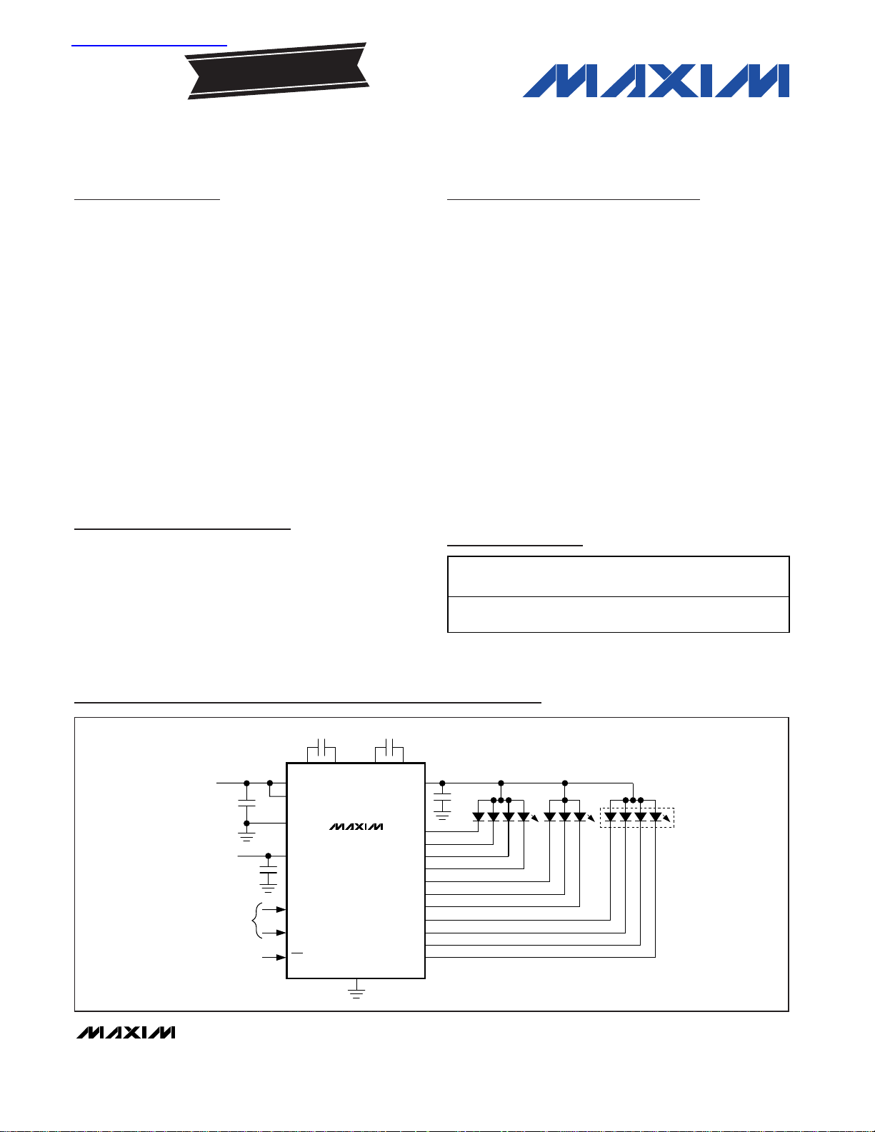
MAX1707
Light-Management IC with Efficient 1x/1.5x/2x
Charge Pump for Backlight/Flash/RGB LEDs
________________________________________________________________ Maxim Integrated Products 1
Ordering Information
MAX1707
1µF1µF
10µF
0.1µF
IN
PIN
SDA
SCK
STB
GND
OUT
C1P C1N
PGND
C2P
FLASH
MAIN
C2N
4.7µF
I
2
C PORT
ON/OFF AND
BRIGHTNESS
INPUT
2.7V TO 5.5V
OUTPUT
UP TO 610mA
M1
M2
M3
M4
S1
S2
S3
F1
F2
F3
F4
STROBE
ON/OFF
V
LOGIC
V
DD
SUB OR RGB
Typical Operating Circuit
19-3744; Rev 0; 7/05
For pricing, delivery, and ordering information, please contact Maxim/Dallas Direct! at
1-888-629-4642, or visit Maxim’s website at www.maxim-ic.com.
Pin Configuration appears at end of data sheet.
EVALUATION KIT
AVAILABLE
PART
PINPACKAGE
PKG
CODE
MAX1707ETG
24 Thin QFN
4mm x 4mm
T2444-4
†
Purchase of I2C components from Maxim Integrated Products,
Inc., or one of its sublicensed Associated Companies, conveys
a license under the Philips I
2
C Patent Rights to use these com-
ponents in an I
2
C system, provided that the system conforms to
the I
2
C Standard Specification as defined by Philips.
查询MAX1707供应商
TEMP RANGE
-40°C to +85°C
Page 2
MAX1707
Light-Management IC with Efficient 1x/1.5x/2x
Charge Pump for Backlight/Flash/RGB LEDs
2 _______________________________________________________________________________________
ABSOLUTE MAXIMUM RATINGS
ELECTRICAL CHARACTERISTICS
(VIN= V
PIN
= VDD= 3.6V, V
GND
= V
PGND
= 0V, temperature derating disabled, TA= -40°C to +85°C, typical values are at TA=
+25°C, unless otherwise noted.) (Note 1)
Stresses beyond those listed under “Absolute Maximum Ratings” may cause permanent damage to the device. These are stress ratings only, and functional
operation of the device at these or any other conditions beyond those indicated in the operational sections of the specifications is not implied. Exposure to
absolute maximum rating conditions for extended periods may affect device reliability.
VDD, IN, PIN, SCK, SDA, STB, OUT to GND .........-0.3V to +6.0V
M_, S_, F_ to GND ....................................-0.3V to (V
OUT
+ 0.3V)
C1N, C2N to GND .......................................-0.3V to (V
IN
+ 0.3V)
C1P, C2P to GND ..-0.3V to greater of (V
OUT
+ 0.3V) or (VIN+ 0.3V)
PGND to GND .......................................................-0.3V to +0.3V
OUT Short Circuit to GND ..........................................Continuous
Continuous Power Dissipation (T
A
= +70°C)
24-Pin Thin QFN (derate 20.8mW/°C above +70°C)...1666mW
Operating Temperature Range ...........................-40°C to +85°C
Junction Temperature......................................................+150°C
Storage Temperature Range .............................-65°C to +150°C
Lead Temperature (soldering, 10s) .................................+300°C
PARAMETER CONDITIONS
UNIT
IN Operating Voltage 2.7 5.5 V
VDD Operating Range 2.7 5.5 V
Undervoltage-Lockout Threshold VIN rising or falling
V
Undervoltage-Lockout Hysteresis 50 mV
Output Overvoltage-Protection Threshold
V
OUT
rising
V
1.5x or 2x mode 4.0 6.5
IN + PIN No-Load Supply Current
10% setting, 1x mode, flash off
mA
TA = +25°C 0.7 5
IN + PIN Shutdown Supply Current
All LEDs off, STB = SDA =
SCK = V
DD
, I2C ready
T
A
= +85°C 0.8
µA
TA = +25°C 0.1 1
VDD Quiescent Current
All LEDs off, STB = SDA =
SCK = V
DD
, I2C ready
T
A
= +85°C 0.1
µA
Startup into 1x mode 0.5
Startup into 1.5x mode 1.0
Soft-Start Time
Startup into 2x mode 1.5
ms
LED Current Derating Function Start
Temperature
Temperature derating enabled
°C
LED Current Derating Function Slope
T
A
= +40°C to +85°C, temperature derating
enabled
%/°C
Default current setting, TA = +25°C -2
+2
LED Current SUB Output Accuracy
(Note 2)
D efaul t cur r ent setti ng , T
A
= - 40°C to + 85°C -5 +5
%
LED Current FLASH and MAIN Output
Accuracy
Default current setting (Note 2) -5
+5 %
M_, S_
Maximum M_, S_, F_ Sink Current
F_ 95
mA
M_, S_ 40 90
LED Dropout Voltage
F_ 40 90
mV
1.5x and 2x Mode Regulation Voltage
mV
1x to 1.5x and 1.5x to 2x Mode Transition
Threshold
V
M_
, VS_, V
F_
falling
mV
MIN TYP MAX
2.25 2.60
4.75 5.00 5.25
100% LED setting (Note 3)
28.5 30.0
0.35
+40
-1.7
±0.3
±0.3
100
150
100
Page 3
MAX1707
Light-Management IC with Efficient 1x/1.5x/2x
Charge Pump for Backlight/Flash/RGB LEDs
_______________________________________________________________________________________ 3
Note 1: All devices are 100% production tested at TA= +25°C. Limits over the operating temperature range are guaranteed
by design.
Note 2: LED current specification includes both accuracy and matching tolerance.
Note 3: Dropout voltage is defined as the M2 or F3 to GND voltage at which current into M2 or F3 drops 10% from the value at 0.2V.
All other current regulators are tested functionally by the accuracy test and guaranteed for low dropout by design.
ELECTRICAL CHARACTERISTICS (continued)
(VIN= V
PIN
= VDD= 3.6V, V
GND
= V
PGND
= 0V, temperature derating disabled, TA= -40°C to +85°C, typical values are at TA=
+25°C, unless otherwise noted.) (Note 1)
PARAMETER CONDITIONS
UNIT
Input Voltage Mode Transition Hysteresis
mV
TA = +25°C
1
M_, S_, F_ Leakage in Shutdown
All LEDs off, STB =
V
DD T
A
= +85°C 0.1
µA
OUT Pulldown Resistance in Shutdown All LEDs off, STB = V
DD
5kΩ
Maximum OUT Current VIN ≥ 3.2V, V
OUT
= 3.9V
mA
1x mode (VIN - V
OUT
) / I
OUT
0.5 2.5
1.5x mode (1.5 x VIN - V
OUT
) / I
OUT
1.5 3.5Open-Loop OUT Resistance
2x mode (2 x V
IN
- V
OUT
) / I
OUT
2.0 4.1
Ω
Switching Frequency 1
MHz
SDA = 111xxx00 2
9
SDA = 111xxx01 2
18
SDA = 111xxx10 2
19
S1, S2, S3 (RGB) Full-Scale Ramp Time
SDA = 111xxx11 2
20
µs
Logic-Input High Voltage VDD = 2.7V to 5.5V
V
Logic-Input Low Voltage VDD = 2.7V to 5.5V 0.4 V
TA = +25°C
1
Logic-Input Current
V
IL
= 0V or VIH =
5.5V
T
A
= +85°C 0.1
µA
SDA Output Low Voltage I
SDA
= 3mA
0.4 V
I2C Clock Frequency 400 kHz
Bus- Fr ee Ti m e Betw een S TART and S TOP
t
BUF
1.3 µs
Hold Time Repeated START Condition t
HD_STA
0.6 0.1 µs
SCK Low Period t
LOW
1.3 0.2 µs
SCK High Period t
HIGH
0.6 0.2 µs
Setup Time Repeated START Condition t
SU_STA
0.6 0.1 µs
SDA Hold Time t
HD_DAT
0
µs
SDA Setup Time t
SU_DAT
50 ns
Setup Time for STOP Condition t
SU_STO
0.6 0.1 µs
Thermal Shutdown
°C
Thermal-Shutdown Hysteresis 20 °C
MIN TYP MAX
150
0.01
610
VDD / 2
0.01
0.03
100
-0.01
+160
Page 4
MAX1707
Light-Management IC with Efficient 1x/1.5x/2x
Charge Pump for Backlight/Flash/RGB LEDs
4 _______________________________________________________________________________________
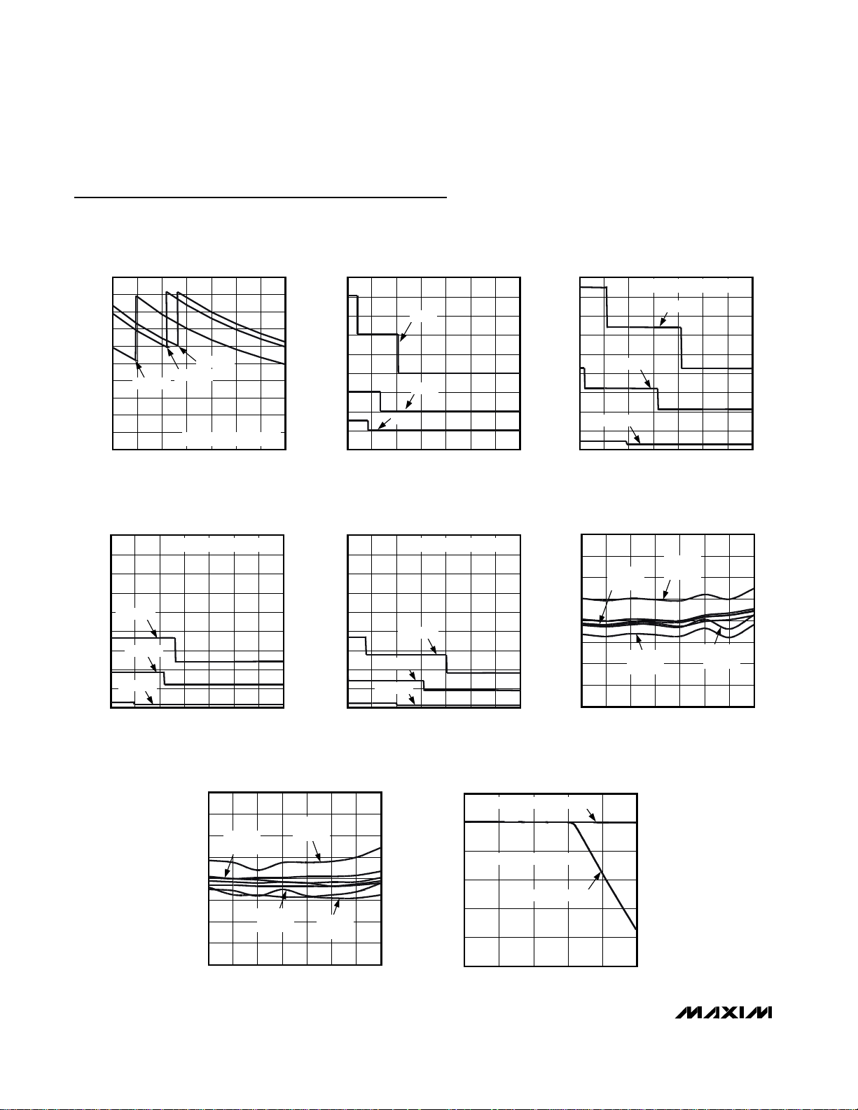
Typical Operating Characteristics
(TA = +25°C, unless otherwise noted.)
MAX1707 toc01
EFFICIENCY vs. SUPPLY VOLTAGE
DRIVING 4 MAIN LEDs
SUPPLY VOLTAGE (V)
EFFICIENCY (%)
4.33.93.53.1
20
10
0
30
40
50
60
70
80
90
100
2.7 5.55.14.7
SUPPLY VOLTAGE FALLING
30mA/LED
15mA/LED
1.9mA/LED
0
200
100
500
400
300
800
700
600
900
2.7 3.9 4.33.1 3.5 4.7 5.1 5.5
INPUT CURRENT vs. SUPPLY VOLTAGE
DRIVING LUMILEDS LXCL-PWF1 FLASH
MAX1707 toc02
SUPPLY VOLTAGE (V)
INPUT CURRENT (mA)
400mA
100mA
200mA
0
100
50
250
200
150
400
350
300
450
2.7 3.9 4.33.1 3.5 4.7 5.1 5.5
INPUT CURRENT vs. SUPPLY VOLTAGE
DRIVING 4 MAIN LEDs AND RGB LEDs
MAX1707 toc03
SUPPLY VOLTAGE (V)
INPUT CURRENT (mA)
SUPPLY VOLTAGE FALLING
30mA/LED
15mA/LED
1.9mA/LED
0
100
50
250
200
150
400
350
300
450
2.7 3.9 4.33.1 3.5 4.7 5.1 5.5
INPUT CURRENT vs. SUPPLY VOLTAGE
DRIVING 4 MAIN LEDs
MAX1707 toc04
SUPPLY VOLTAGE (V)
INPUT CURRENT (mA)
1.9mA/LED
SUPPLY VOLTAGE FALLING
30mA/LED
15mA/LED
0
100
50
250
200
150
400
350
300
450
2.7 3.9 4.33.1 3.5 4.7 5.1 5.5
INPUT CURRENT vs. SUPPLY VOLTAGE
DRIVING RGB LEDs
MAX1707 toc05
SUPPLY VOLTAGE (V)
INPUT CURRENT (mA)
SUPPLY VOLTAGE FALLING
30mA/LED
15mA/LED
1.9mA/LED
LED CURRENT MATCHING
vs. SUPPLY VOLTAGE
(MAIN AND RGB AT FULL CURRENT)
MAX1707 toc06
28.8
29.4
29.1
30.6
30.9
30.3
30.0
29.7
31.2
LED CURRENT (mA)
2.7 3.9 4.33.1 3.5 4.7 5.1 5.5
SUPPLY VOLTAGE (V)
4 WHITE
V
F
= 3.4V
RED
V
F
= 1.9V
GREEN
V
F
= 2V
BLUE
V
F
= 4.2V
LED CURRENT MATCHING
vs. SUPPLY VOLTAGE
(MAIN AND RGB AT 1.9mA/LED)
MAX1707 toc07
1.80
1.84
1.82
1.92
1.94
1.90
1.88
1.86
1.96
LED CURRENT (mA)
2.7 3.9 4.33.1 3.5 4.7 5.1 5.5
SUPPLY VOLTAGE (V)
4 WHITE
V
F
= 2.9V
RED
V
F
= 1.7V
GREEN
V
F
= 1.9V
BLUE
V
F
= 3.4V
0
10
5
20
15
25
30
-40 85
LED CURRENT vs. TEMPERATURE
MAX1707 toc08
TEMPERATURE (°C)
LED CURRENT (mA)
10-15 35 60
THERMAL DERATING OFF
THERMAL DERATING ON
4 MAIN OR 4 FLASH LEDs
Page 5
MAX1707
Light-Management IC with Efficient 1x/1.5x/2x
Charge Pump for Backlight/Flash/RGB LEDs
_______________________________________________________________________________________ 5
50mV/div
(AC-COUPLED)
100mA/div
0
I
IN
50mV/div
(AC-COUPLED)
V
OUT
V
IN
1µs/div
OPERATING WAVEFORMS 1X MODE
MAX1707 toc09
50mV/div
(AC-COUPLED)
100mA/div
0
I
IN
50mV/div
(AC-COUPLED)
V
OUT
V
IN
1µs/div
OPERATING WAVEFORMS 1.5X MODE
MAX1707 toc10
50mV/div
(AC-COUPLED)
100mA/div
0
I
IN
50mV/div
(AC-COUPLED)
V
OUT
V
IN
1µs/div
OPERATING WAVEFORMS 2X MODE
MAX1707 toc11
200mA/div
0
0
I
IN
5V/div
1V/div
V
OUT
V
SDA
1ms/div
MAIN BACKLIGHT STARTUP WAVEFORM
MAX1707 toc12
200mA/div
0
0
I
IN
5V/div
1V/div
V
OUT
V
SDA
1ms/div
MAIN STARTUP WITH RGB ALREADY ON
MAX1707 toc13
200mA/div
0
0
I
IN
5V/div
1V/div
V
OUT
V
SDA
1ms/div
FLASH STARTUP WAVEFORM
MAX1707 toc14
Typical Operating Characteristics (continued)
(TA = +25°C, unless otherwise noted.)
Page 6

MAX1707
Light-Management IC with Efficient 1x/1.5x/2x
Charge Pump for Backlight/Flash/RGB LEDs
6 _______________________________________________________________________________________
200mA/div
0
0
I
IN
5V/div
1V/div
V
OUT
V
STB
1ms/div
STROBE STARTUP WAVEFORM
WITH MAIN ALREADY ON
MAX1707 toc15
100mA/div
0
0
I
OUT
5V/div
1V/div
V
OUT
V
SDA
1ms/div
MAIN BRIGHTNESS CHANGE
(1.9mA/LED TO 30mA/LED)
MAX1707 toc16
200mA/div
0
I
OUT
1V/div
4V
1V/div
V
OUT
V
IN
100µs/div
LINE-TRANSIENT RESPONSE
(4V TO 3.3V TO 4V)
MAX1707 toc17
200mA/div
0
I
OUT
1V/div
4V
1V/div
V
OUT
V
IN
100µs/div
LINE-TRANSIENT RESPONSE WITH
MODE TRANSITION (3.3V TO 2.7V TO 3.3V)
MAX1707 toc18
20mA/div
0
0
I
BLUE
20mA/div
0
20mA/div
I
GREEN
I
RED
200ms/div
RGB RAMP WAVEFORMS
(BLUE-TO-YELLOW TRANSITION)
MAX1707 toc19
FULL-BRIGHTNESS
1048ms RAMP TIME
10mA/div
0
0
I
BLUE
10mA/div
0
10mA/div
I
GREEN
I
RED
40ms/div
RGB RAMP WAVEFORMS
(BLUE-TO-YELLOW TRANSITION)
MAX1707 toc20
HALF-BRIGHTNESS
DEFAULT RAMP TIME
Typical Operating Characteristics (continued)
(TA = +25°C, unless otherwise noted.)
Page 7

MAX1707
Light-Management IC with Efficient 1x/1.5x/2x
Charge Pump for Backlight/Flash/RGB LEDs
_______________________________________________________________________________________ 7
Pin Description
PIN NAME FUNCTION
1PIN
Power-Supply Voltage Input. Connect PIN to IN. Connect a 4.7µF ceramic capacitor from PIN to
PGND. The input voltage range is 2.7V to 5.5V. PIN is high impedance during shutdown.
2IN
Analog Supply Voltage Input. Connect IN to PIN. The input voltage range is 2.7V to 5.5V. IN is high
impedance during shutdown.
3 GND
Ground. Connect GND to system ground and the ground side of the input bypass capacitor as close
to the IC as possible.
4V
DD
Logic-Input Supply Voltage. Connect VDD to the logic supply driving SDA, SCK, and STB. Connect a
0.1µF ceramic capacitor from V
DD
to GND.
5M4
6M3
7M2
8M1
9F4
10 F3
11 F2
12 F1
13 S3
14 S2
15 S1
LED Cathode Connections. Current flowing into these pins is based on the internal I
2
C dimming
registers. The charge pump regulates the lowest LED cathode voltage to 0.15V. Grounding any of
these pins forces output overvoltage protection mode causing OUT to pulse on and off at
approximately 5V. To avoid constantly operating in overvoltage protection mode, any unused LED
cathode connection (M_, S_, or F_) must be connected to OUT. This disables the corresponding
current regulator. These pins are high impedance in shutdown.
M1 through M4 are for main display backlights.
S1 through S3 are for subdisplay backlights or one RGB LED indicator.
F1 through F4 are for LED flash.
Any combination of M_, S_, and F_ can be connected together to drive higher current LEDs.
16 STB
Strobe Logic Input. Drive STB low to turn on the flash LEDs (F1, F2, F3, F4) at the current specified in
the internal strobe register. Drive STB high to turn off the flash LEDs. Connect to V
DD
if the flash LEDs
are turned on/off only by the I
2
C interface.
17 SCK I2C Clock Input. Data is read on the rising edge of SCK.
18 SDA I2C Data Input. Data is read on the rising edge of SCK.
19 C1N
Transfer Capacitor 1 Negative Connection. Connect a 1µF ceramic capacitor from C1N to C1P. C1N
is shorted to IN during shutdown.
20 C1P
Transfer Capacitor 1 Positive Connection. Connect a 1µF ceramic capacitor from C1N to C1P. During
shutdown, if V
OUT
> V
IN
, C1P is shorted to OUT. If V
OUT
< V
IN
, C1P is shorted to IN.
21 PGND
Power Ground. Charge-pump switching ground. Connect to GND and EP as close to the IC as
possible.
22 OUT
Output. Connect a 10µF ceramic capacitor from OUT to PGND. The anodes of all the LEDs connect
to OUT. OUT is pulled to ground through an internal 5kΩ resistor in
shutdown.
23 C2P
Transfer Capacitor 2 Positive Connection. Connect a 1µF ceramic capacitor from C2N to C2P. During
shutdown, if V
OUT
> VIN, C2P is shorted to OUT. If V
OUT
< VIN, C2P is shorted to IN.
24 C2N
Transfer Capacitor 2 Negative Connection. Connect a 1µF ceramic capacitor from C2N to C2P. C2N
is shorted to IN during shutdown.
—EPExposed Paddle. Connect to GND and PGND directly under the IC.
Page 8

MAX1707
Light-Management IC with Efficient 1x/1.5x/2x
Charge Pump for Backlight/Flash/RGB LEDs
8 _______________________________________________________________________________________
BRIGHTNESS CONTROL
STB CONTROL
SELECT
MIN
ERROR
AMP 1
I2C AND
CONTROL
MAX1707
SCK
S1
D1
S2
D2
S3
D3
+
–
+
–
+
–
INPUT
2.7V TO 5.5V
2.7V TO 5.5V
1.25V
OUT
OUT
OVP
C
IN
4.7µF
C
VDD
0.1µF
C
OUT
10µF
ERROR
AMP 2
R
SET
M1
D4
M2
D5
M3
D6
M4
D7
+
–
+
–
+
–
+
–
SDA
STB
V
DD
C1
1µF
C1P
PIN
PGND
IN
C1N C2P C2N
C2
1µF
1x/1.5x/2x REGULATING
CHARGE PUMP
GND
REFERENCE
0.15V
0.6V
F1
D8
F2
D9
F3
D10
F4
D11
+
–
+
–
+
–
+
–
Figure 1. Functional Diagram
Page 9

Detailed Description
The MAX1707 charge pump operates in three modes to
maintain high efficiency over a wide supply voltage
range. The IC automatically selects between these
three modes as described in the 1x/1.5x/2x Mode
Switchover section.
Current-sinking LED cathode connections are provided
to drive four main (M_) and three sub (S_) LEDs at a
regulated current up to 30mA each. The sub LED connections can be used for either subdisplay backlighting
or one RGB indicator. The IC also contains four flash
LED connections (F_) that sink up to 100mA each.
These LED connections can be connected together in
any combination to provide increased current up to
610mA total.
An I2C serial port is used for on/off control and setting
the LED currents in 32 linear steps. When using the
RGB indicator, the I2C port provides 32k colors and
programmable ramp-up/down rates. The camera flash
can be turned on/off by the I2C port or a separate digital logic input with either method programmed to its
own brightness level.
1x/1.5x/2x Mode Switchover
When the input voltage is higher than the required output voltage needed to drive the LEDs, the MAX1707
pulls OUT up to the input voltage (in 1x mode), while
still regulating the LED current with the current regulators. As the input voltage drops, the lowest LED cathode voltage falls below the 100mV switchover
threshold, and the MAX1707 starts switching in 1.5x
mode. When the input voltage is rising, the transition
from 1.5x to 1x is made when VINis greater than V
OUT
.
When the MAX1707 is running in 1.5x mode and the
input voltage is decreased, the lowest LED cathode
voltage crosses the 100mV switchover threshold again.
At this point, the MAX1707 changes to the 2x chargepump mode. With the input voltage rising and the
MAX1707 in 2x mode, the IC changes to 1.5x mode
once VINis greater than 2/3 of the output voltage.
Soft-Start
The MAX1707 includes soft-start circuitry to limit inrush
current at turn-on and mode transitions. When starting
up, the output capacitor is charged directly from the
input with a ramped current source (with no chargepump action) until the output voltage is near the input
voltage. After 512µs, if all the LED cathodes are not
above 100mV, the MAX1707 switches to 1.5x mode
with the LED output current ramped from 1/32 to the
programmed current in 1/32 steps. After another 512µs,
if all the LED cathodes are not above 100mV, the
MAX1707 switches to 2x mode, once again ramping
the LED current from 1/32 to the programmed current in
1/32 steps. Any time the output voltage is less than
1.25V, the soft-start routine is reset to the 1x state. Thus,
the startup time is 512µs, 1024µs, or 1536µs, depending
on what mode is required after the completion of startup.
Output-Current Settings
The output currents for the main, sub, and flash current
regulators are set using the I2C serial interface (see the
I2C Interface section). The current for the four main
LEDs is always equal and set with a single command.
The currents for the three sub LEDs are set independently, allowing them to drive an RGB LED. The current-level settings for both the main and sub LEDs
range from 0.9mA to 30mA, defaulting to 15mA each
(see Tables 1, 2, and 3).
MAX1707
Light-Management IC with Efficient 1x/1.5x/2x
Charge Pump for Backlight/Flash/RGB LEDs
_______________________________________________________________________________________ 9
Table 1. Control Data Byte
SDA CONTROL BYTE
COMMAND DATA
FUNCTION
C2 C1 C0 D4 D3 D2 D1 D0
On/Off Control 0 0 0 Main Sub3 Sub2 Sub1 Flash
Main Brightness 0 0 1 32 steps, 30mA/LED max
Sub1 Brightness 0 1 0 32 steps, 30mA max
Sub2 Brightness 0 1 1 32 steps, 30mA max
Sub3 Brightness 1 0 0 32 steps, 30mA max
Flash Brightness 1 0 1 32 steps, 100mA/LED max, I2C enable
Strobe Brightness 1 1 0 32 steps, 100mA/LED max, STB enable
Other Functions 1 1 1 X X
Temp
Derate
RGB Ramp Rate
Note: C2 is MSB and D0 is LSB. X = Don’t care.
Page 10

MAX1707
Light-Management IC with Efficient 1x/1.5x/2x
Charge Pump for Backlight/Flash/RGB LEDs
10 ______________________________________________________________________________________
Table 2. Data and LED Currents
DATA LED CURRENT (mA)
D4 D3 D2 D1 D0 MAIN SUB1 SUB2 SUB3
STROBE
000000.90.9 0.9 0.9 3.3 3.3
000011.91.9 1.9 1.9 6.5 6.5
000102.82.8 2.8 2.8 9.7 9.7
000113.8 3.8 3.8 3.8 12.9 12.9
001004.7 4.7 4.7 4.7 16.2 16.2
001015.6 5.6 5.6 5.6 19.4 19.4
001106.6 6.6 6.6 6.6 22.6 22.6
001117.57.5 7.5 7.5 25.8 25.8
010008.4 8.4 8.4 8.4 28.9 28.9
010019.4 9.4 9.4 9.4 32.1 32.1
0101010.3 10.3 10.3 10.3 35.4 35.4
0101111.3 11.3 11.3 11.3 38.6 38.6
0110012.2 12.2 12.2 12.2 41.6 41.6
0110113.1 13.1 13.1 13.1 44.7 44.7
0111014.1 14.1 14.1 14.1 47.9 47.9
0111115.0 15.0 15.0 15.0 51.0 51.0
1000015.9 15.9 15.9 15.9 54.1 54.1
1000116.9 16.9 16.9 16.9 57.2 57.2
1001017.8 17.8 17.8 17.8 60.3 60.3
1001118.8 18.8 18.8 18.8 63.4 63.4
1010019.7 19.7 19.7 19.7 66.3 66.3
1010120.6 20.6 20.6 20.6 69.6 69.6
1011021.6 21.6 21.6 21.6 72.7 72.7
1011122.5 22.5 22.5 22.5 75.8 75.8
1100023.4 23.4 23.4 23.4 78.8 78.8
1100124.4 24.4 24.4 24.4 81.9 81.9
1101025.3 25.3 25.3 25.3 84.9 84.9
1101126.3 26.3 26.3 26.3 87.9 87.9
1110027.2 27.2 27.2 27.2 91.0 91.0
1110128.1 28.1 28.1 28.1 94.0 94.0
1111029.1 29.1 29.1 29.1 97.0 97.0
1111130.0 30.0 30.0 30.0 100.0 100.0
Note: Defaults in bold.
FLASH
Page 11

MAX1707
Light-Management IC with Efficient 1x/1.5x/2x
Charge Pump for Backlight/Flash/RGB LEDs
______________________________________________________________________________________ 11
Table 3. Control Data Byte (Hexadecimal)
CONTROL BYTE (HEXADECIMAL) LED CURRENT (mA)
MAIN
STROBE
20 40 60 80 A0 C0 0.9 0.9 0.9 0.9 3.3 3.3
21 41 61 81 A1 C1 1.9 1.9 1.9 1.9 6.5 6.5
22 42 62 82 A2 C2 2.8 2.8 2.8 2.8 9.7 9.7
23 43 63 83 A3 C3 3.8 3.8 3.8 3.8 12.9 12.9
24 44 64 84 A4 C4 4.7 4.7 4.7 4.7 16.2 16.2
25 45 65 85 A5 C5 5.6 5.6 5.6 5.6 19.4 19.4
26 46 66 86 A6 C6 6.6 6.6 6.6 6.6 22.6 22.6
27 47 67 87 A7 C7 7.5 7.5 7.5 7.5 25.8 25.8
28 48 68 88 A8 C8 8.4 8.4 8.4 8.4 28.9 28.9
29 49 69 89 A9 C9 9.4 9.4 9.4 9.4 32.1 32.1
2A 4A 6A 8A AA CA 10.3 10.3 10.3 10.3 35.4 35.4
2B 4B 6B 8B AB CB 11.3 11.3 11.3 11.3 38.6 38.6
2C 4C 6C 8C AC CC 12.2 12.2 12.2 12.2 41.6 41.6
2D 4D 6D 8D AD CD 13.1 13.1 13.1 13.1 44.7 44.7
2E 4E 6E 8E AE CE 14.1 14.1 14.1 14.1 47.9 47.9
2F 4F 6F 8F AF CF 15.0 15.0 15.0 15.0 51.0 51.0
30 50 70 90 B0 D0 15.9 15.9 15.9 15.9 54.1 54.1
31 51 71 91 B1 D1 16.9 16.9 16.9 16.9 57.2 57.2
32 52 72 92 B2 D2 17.8 17.8 17.8 17.8 60.3 60.3
33 53 73 93 B3 D3 18.8 18.8 18.8 18.8 63.4 63.4
34 54 74 94 B4 D4 19.7 19.7 19.7 19.7 66.3 66.3
35 55 75 95 B5 D5 20.6 20.6 20.6 20.6 69.6 69.6
36 56 76 96 B6 D6 21.6 21.6 21.6 21.6 72.7 72.7
37 57 77 97 B7 D7 22.5 22.5 22.5 22.5 75.8 75.8
38 58 78 98 B8 D8 23.4 23.4 23.4 23.4 78.8 78.8
39 59 79 99 B9 D9 24.4 24.4 24.4 24.4 81.9 81.9
3A 5A 7A 9A BA DA 25.3 25.3 25.3 25.3 84.9 84.9
3B 5B 7B 9B BB DB 26.3 26.3 26.3 26.3 87.9 87.9
3C 5C 7C 9C BC DC 27.2 27.2 27.2 27.2 91.0 91.0
3D 5D 7D 9D BD DD 28.1 28.1 28.1 28.1 94.0 94.0
3E 5E 7E 9E BE DE 29.1 29.1 29.1 29.1 97.0 97.0
3F 5F 7F 9F BF DF 30.0 30.0 30.0 30.0
100.0
Note: Defaults in bold.
SUB1 SUB2 SUB3 FLASH STROBE MAIN SUB1 SUB2 SUB3 FLASH
100.0
Page 12

MAX1707
The flash LEDs are controlled either using the I2C interface or by pulsing the STB input low. There are two registers in the MAX1707 to set the flash current level. The
FLASH register sets the LED current when the I2C interface is used to pulse the flash LEDs, and the STROBE
register sets the LED current when the STB input is
pulsed. The current-level settings for the flash LEDs
range from 3.3mA to 100mA, with a default of 25.8mA
(see Tables 1, 2, and 3). The strobe register has priority
over the flash register when both strobe and flash are on.
The LED cathode connections (M_, S_, and F_) can be
connected together in any combination to allow the use
of higher current LEDs. For example, to drive a single
flash LED at up to 400mA, connect F1, F2, F3, and F4
together to the cathode of the flash LED.
To avoid constantly operating in overvoltage protection
mode, any unused LED cathode connection (M_, S_, or
F_) must be connected to OUT. This disables the corresponding current regulator.
RGB Color and Ramp-Rate Settings
The three sub LED currents are controlled independently by the I
2
C interface, allowing for use of a com-
mon anode RGB LED. Thirty-two programmable brightness levels (5 bits) per LED provide a total of 32k colors. To smooth the transition between different
color/brightness settings, a controlled ramp is used
when the sub LED current level is changed, when the
sub LEDs are enabled, and when the LEDs are disabled. The ramp rate is set to one of four settings with
the I
2
C interface (see Table 4).
Temperature-Derating Function
The MAX1707 contains a temperature-derating function
that automatically limits the LED current at high temperatures in accordance with the recommended derating
curve of popular white LEDs. The derating function
enables the safe usage of higher LED current at room
temperature, thus reducing the number of LEDs required
to backlight the display. In camera-light applications, the
derating circuit protects the LEDs and PC board from
overheating. The derating circuit limits the LED current
by reducing the LED current above +40°C by approximately 1.7%/°C. The typical derating function characteristic is shown in the Typical Operating Characteristics.
The temperature derating function is enabled/disabled
using the I
2
C interface and is off by default.
I2C Interface
An I2C 2-wire serial interface is provided on the
MAX1707 to control LED brightness, flash, temperature
deration, and RGB ramp rate. The serial interface consists of a serial data line (SDA) and a serial clock line
(SCK). Standard I2C write-byte commands are used.
Figure 2 shows a timing diagram for the I2C protocol.
The MAX1707 is a slave-only device, relying upon a
master to generate a clock signal. The master (typically
a microprocessor) initiates data transfer on the bus and
Light-Management IC with Efficient 1x/1.5x/2x
Charge Pump for Backlight/Flash/RGB LEDs
12 ______________________________________________________________________________________
Table 4. RGB Ramp Rate
CONTROL BYTE
(HEXADECIMAL)
RGB RAMP
R A M P TI M E FR O M OF F T O
F U L L BR I G H T N ESS ( m s )
E0 58.6 0.512
E1 0.114 262
E2 0.0572 524
E3 0.0286 1048
Figure 2. I2C Timing Diagram
*Default in bold.
RATE (A/s)
AB CDEFG HIJK
SCK
SDA
t
t
SU:STA
HD:STA
A = START CONDITION
B = MSB OF ADDRESS CLOCKED INTO SLAVE
C = LSB OF ADDRESS CLOCKED INTO SLAVE
D = R/W BIT CLOCKED INTO SLAVE
E = SLAVE PULLS SMBDATA LINE LOW
t
t
LOW
HIGH
t
SU:DAT
F = ACKNOWLEDGE BIT CLOCKED INTO MASTER
G = MSB OF DATA CLOCKED INTO SLAVE (OP/SUS BIT)
H = LSB OF DATA CLOCKED INTO SLAVE
I = SLAVE PULLS SMBDATA LINE LOW
t
HD:DAT
L M
t
t
SU:STO
BUF
J = ACKNOWLEDGE CLOCKED INTO MASTER
K = ACKNOWLEDGE CLOCK PULSE
L = STOP CONDITION, DATA EXECUTED BY SLAVE
M = NEW START CONDITION
Page 13

generates SCK to permit data transfer. A master device
communicates to the MAX1707 by transmitting the
proper 8-bit address (0x9A) followed by the 8-bit control byte. Each 8-bit control byte consists of a 3-bit
command code and 5 bits of data (see Table 1). Each
transmit sequence is framed by a START (A) condition
and a STOP (L) condition (see Figure 2). Each word
transmitted over the bus is 8 bits long and is always followed by an acknowledge clock pulse.
Shutdown Mode
When all the LEDs are off, the MAX1707 turns off the
charge pump and enters low-power shutdown mode.
When in shutdown, OUT is pulled to GND by an internal
5kΩ resistor, discharging the output capacitor. IN and
PIN are high impedance during shutdown, but the I2C
interface (powered from VDD) remains active. To enter
shutdown, send control byte 0x00 to the I2C interface,
and drive STB high. To exit shutdown, enable any of
the LEDs with the I2C interface or STB input.
STB
Logic Input
The STB input is used to control the flash LEDs without
accessing the I2C interface. When STB is driven low,
the flash LEDs are driven to the current set in the
STROBE register. Driving STB low overrides the flash
register settings. With STB high, the flash LEDs are
controlled by the I2C interface flash register and on/off
control.
Output Overvoltage Protection
In case an LED fails or the cathode is shorted to GND,
the output overvoltage protection limits the output to
5V. When the MAX1707 detects the output voltage rising above 5V, it shuts off the charge pump. The charge
pump restarts once the output voltage has dropped to
4.9V.
To avoid constantly operating in overvoltage protection,
any unused LED cathode connection (M_, S_, or F_)
must be connected to OUT; this disables the corresponding current regulator.
Thermal Shutdown
Thermal shutdown limits total power dissipation in the
MAX1707. When the junction temperature exceeds
+160°C, the MAX1707 turns off, allowing the IC to cool.
The MAX1707 turns on and begins soft-start after the junction temperature cools by 20°C. This results in a pulsed
output during continuous thermal-overload conditions.
Applications Information
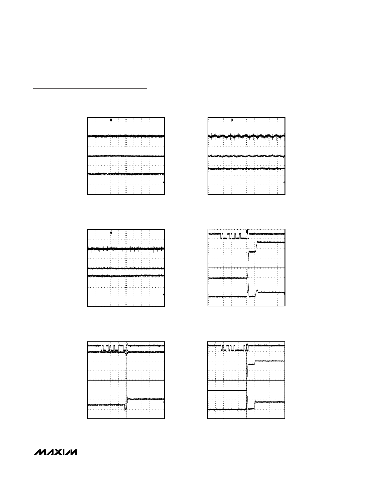
Input Ripple
In 1x mode, the input ripple of the MAX1707 is negligible. When the charge pump is switching in 1.5x or 2x
mode, the input ripple depends on the load current and
the output impedance of the source supply. The worstcase ripple occurs when the charge pump is operating
in 1.5x mode. The switching waveforms in the Typical
Operating Characteristics show the typical input ripple.
For noise-sensitive applications, input ripple can be
reduced by increasing the input capacitance.
Capacitor Selection
Ceramic capacitors are recommended due to their small
size, low cost, and low ESR. Select ceramic capacitors
that maintain their capacitance over temperature and DC
bias. Capacitors with X5R or X7R temperature characteristics generally perform well. Recommended values are
shown in the Typical Operating Circuit. Using a larger-
value input capacitor helps to reduce input ripple (see
the Input Ripple section).
PC Board Layout and Routing
The MAX1707 is a high-frequency switched-capacitor
regulator. For best circuit performance, use a solid
ground plane and place the capacitors as close to the
IC as possible. Connect the exposed pad to GND and
PGND, and allow sufficient copper area for cooling the
IC. Refer to the MAX1707 evaluation kit for an example
PC board layout.
MAX1707
Light-Management IC with Efficient 1x/1.5x/2x
Charge Pump for Backlight/Flash/RGB LEDs
______________________________________________________________________________________ 13
23
24
22
21
8
7
9
IN
V
DD
M4
M3
10
PIN
SCK
S1
S2
SDA
S3
12
OUT
456
1718 16 14 13
C2P
C2N
F3
F4
M1
M2
MAX1707ETG
GND
STB
3
15
PGND
20
11
F2
C1P
19
12
F1
C1N
THIN QFN
4mm x 4mm
TOP VIEW
Pin Configuration
Chip Information
PROCESS: BiCMOS
Page 14

MAX1707
Light-Management IC with Efficient 1x/1.5x/2x
Charge Pump for Backlight/Flash/RGB LEDs
14 ______________________________________________________________________________________
Package Information
(The package drawing(s) in this data sheet may not reflect the most current specifications. For the latest package outline information
go to www.maxim-ic.com/packages
.)
24L QFN THIN.EPS
PACKAGE OUTLINE,
21-0139
2
1
E
12, 16, 20, 24, 28L THIN QFN, 4x4x0.8mm
Page 15

MAX1707
Light-Management IC with Efficient 1x/1.5x/2x
Charge Pump for Backlight/Flash/RGB LEDs
Maxim cannot assume responsibility for use of any circuitry other than circuitry entirely embodied in a Maxim product. No circuit patent licenses are
implied. Maxim reserves the right to change the circuitry and specifications without notice at any time.
Maxim Integrated Products, 120 San Gabriel Drive, Sunnyvale, CA 94086 408-737-7600 ____________________ 15
© 2005 Maxim Integrated Products Printed USA is a registered trademark of Maxim Integrated Products, Inc.
Package Information (continued)
(The package drawing(s) in this data sheet may not reflect the most current specifications. For the latest package outline information
go to www.maxim-ic.com/packages
.)
PACKAGE OUTLINE,
21-0139
2
2
E
12, 16, 20, 24, 28L THIN QFN, 4x4x0.8mm
 Loading...