Maxim MAX17019, MAX17019ATM+ Datasheet
General Description
The MAX17019 is a high-input-voltage quad-output controller (up to 38V). The MAX17019 provides a compact,
low-cost controller capable of providing four independent regulators—a main stage, a 3A
P-P
internal step-
down, a 5A
P-P
internal step-down, and a 2A source/sink
linear regulator. The input voltage is up to 38V. This
makes it an excellent choice for automotive applications.
The internal switching regulators include 5V synchronous
MOSFETs that can be powered directly from a single Li+
cell or from the main 3.3V/5V power stages. Finally, the
linear regulator is capable of sourcing and sinking 2A to
support DDR termination requirements or to generate a
fixed output voltage.
The step-down converters use a peak current-mode,
fixed-frequency control scheme—an easy to implement
architecture that does not sacrifice fast-transient
response. This architecture also supports peak currentlimit protection and pulse-skipping operation to maintain
high efficiency under light-load conditions.
Separate enable inputs and independent open-drain
power-good outputs allow flexible power sequencing. A
soft-start function gradually ramps up the output voltage to reduce the inrush current. Disabled regulators
enter high-impedance states to avoid negative output
voltage created by rapidly discharging the output
through the low-side MOSFET. The MAX17019 also
includes output undervoltage, output overvoltage, and
thermal-fault protection.
The MAX17019 is available in a 48-pin, 6mm x 6mm
thin QFN package.
Applications
Automotive Battery-Powered Devices
Embedded Control Systems
Set-Top Boxes
Features
♦ Fixed-Frequency, Current-Mode Controllers
♦ 5.5V to 38V Input Range (Step-Down)
♦ 1x Step-Down Controller
♦ 1x Internal 5A
P-P
Step-Down Regulator
♦ 1x Internal 3A
P-P
Step-Down Regulator
♦ 1x 2A Source/Sink Linear Regulator with Dynamic
REFIN
♦ Internal BST Diodes
♦ Internal 5V 50mA Linear Regulator
♦ Fault Protection—Undervoltage, Overvoltage,
Thermal, Peak Current Limit
♦ Independent Enable Inputs and Power-Good
Outputs
♦ Voltage-Controlled Soft-Start
♦ High-Impedance Shutdown
♦ 10µA (typ) Shutdown Current
MAX17019
High-Input-Voltage Quad-Output Controller
________________________________________________________________
Maxim Integrated Products
1
MAX17019
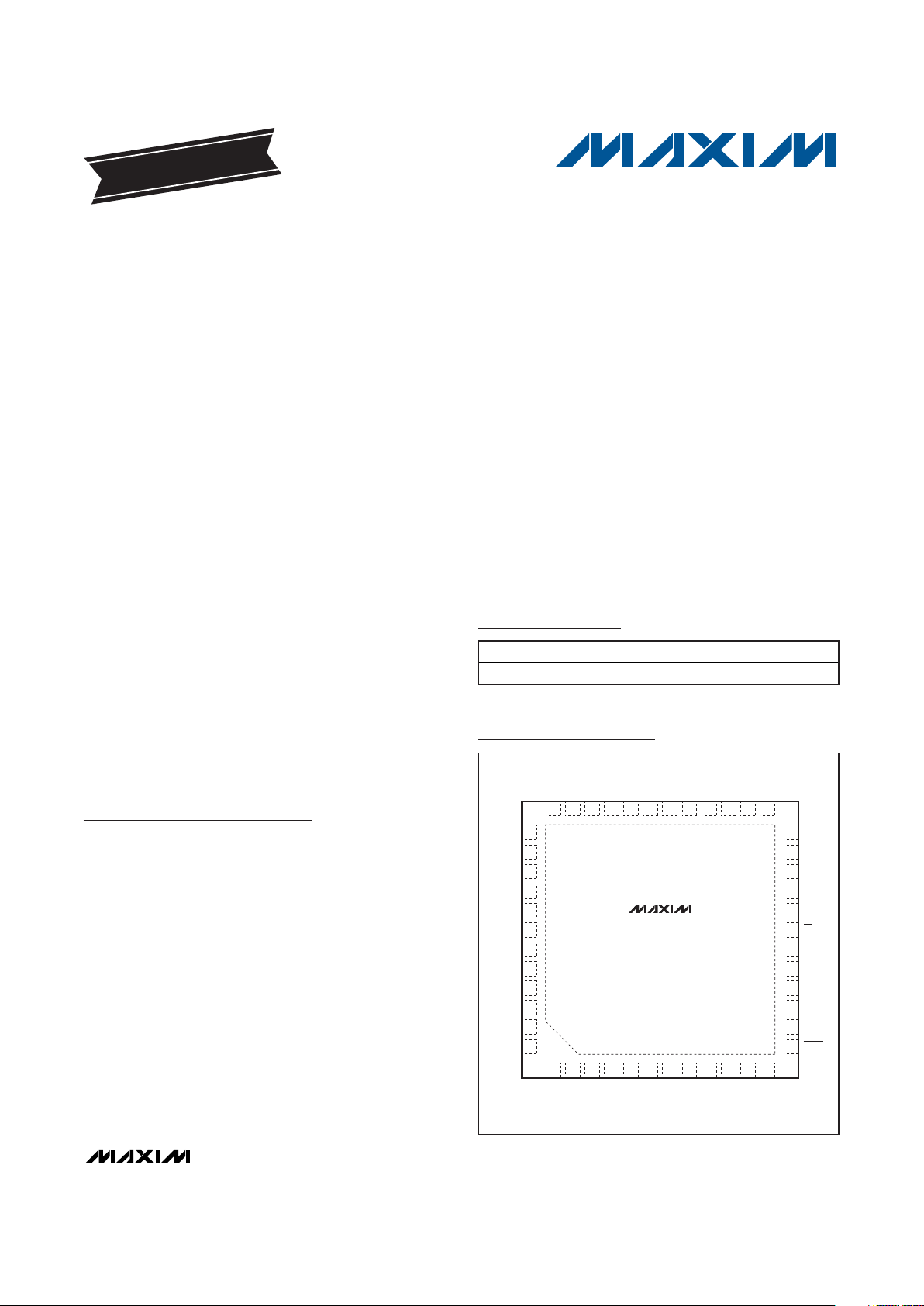
36 35 34 33 32 31 30 29 28 27 26 25
24
23
22
21
20
19
18
17
16
15
14
13
CSPA
CSNA
AGND
REF
FREQ
UP/DN
INA
V
CC
BYP
LDO5
INLDO
SHDN
ONB
SYNC
ONA
INBC
INBC
INBC
INBC
V
DD
POKD
OND
ONC
FBC
37
38
39
40
41
42
43
44
45
46
47
48
1
POKC
BSTC
LXC
LXC
LXC
LXC
OUTD
OUTD
IND
FBD
VTTR
REFIND
FBB
POKB
BSTB
LXB
LXB
LXB
DLA
BSTA
LXA
DHA
POKA
FBA
+
2 3 4 5 6 7 8 9 10 11 12
EXPOSED PAD = PGND
THIN QFN
TOP VIEW
Pin Configuration
19-4225; Rev 0; 8/08
For pricing, delivery, and ordering information, please contact Maxim Direct at 1-888-629-4642,
or visit Maxim’s website at www.maxim-ic.com.
EVALUATION KIT
AVAILABLE
Ordering Information
+
Denotes a lead-free/RoHS-compliant package.
*
EP = Exposed pad.
PART TEMP RANGE PIN-PACKAGE
MAX17019ATM+ -40°C to +125°C 48 TQFN-EP*
MAX17019
High-Input-Voltage Quad-Output Controller
2 _______________________________________________________________________________________
ABSOLUTE MAXIMUM RATINGS
ELECTRICAL CHARACTERISTICS
(Circuit of Figure 1, V
INLDO
= 12V, V
INA
= V
INBC
= VDD= VCC= V
BYP
= V
CSPA
= V
CSNA
= 5V, V
IND
= 1.8V, V
SHDN
= V
ONA
= V
ONB
=
V
ONC
= V
OND
= 5V, I
REF
= I
LDO5
= I
OUTD
= no load, FREQ = GND, UP/DN = VCC, TA= 0°C to +85°C, unless otherwise noted.
Typical values are at T
A
= +25°C.) (Note 1)
Stresses beyond those listed under “Absolute Maximum Ratings” may cause permanent damage to the device. These are stress ratings only, and functional
operation of the device at these or any other conditions beyond those indicated in the operational sections of the specifications is not implied. Exposure to
absolute maximum rating conditions for extended periods may affect device reliability.
INLDO, SHDN to GND............................................-0.3V to +43V
LDO5, INA, V
DD
, VCCto GND..................................-0.3V to +6V
DHA to LXA .............................................-0.3V to (V
BSTA
+ 0.3V)
ONA, ONB, ONC, OND to GND ...............................-0.3V to +6V
POKA, POKB, POKC, POKD to GND.........-0.3V to (V
CC
+ 0.3V)
REF, REFIND, FREQ, UP/DN,
SYNC to GND ........................................-0.3V to (V
CC
+ 0.3V)
FBA, FBB, FBC, FBD to GND.....................-0.3V to (V
CC
+ 0.3V)
BYP to GND ............................................-0.3V to (V
LDO5
+ 0.3V)
CSPA, CSNA to GND .................................-0.3V to (V
CC
+ 0.3V)
DLA to GND................................................-0.3V to (V
DD
+ 0.3V)
INBC, IND to GND....................................................-0.3V to +6V
OUTD to GND............................................-0.3V to (V
IND
+ 0.3V)
VTTR to GND.............................................-0.3V to (V
BYP
+ 0.3V)
LXB, LXC to GND ....................................-1.0V to (V
INBC
+ 0.3V)
BSTB to GND ....................................(V
DD
- 0.3V) to (V
LXB
+ 6V)
BSTC to GND....................................(V
DD
- 0.3V) to (V
LXC
+ 6V)
BSTA to GND ....................................(V
DD
- 0.3V) to (V
LXA
+ 6V)
REF Short-Circuit Current......................................................1mA
Continuous Power Dissipation (T
A
= +70°C)
Multilayer PCB: 48-Pin 6mm x 6mm
2
TQFN
(T4866-2 derated 37mW/°C above +70°C) ....................2.9W
Operating Temperature Range .........................-40°C to +105°C
Junction Temperature......................................................+150°C
Storage Temperature Range .............................-65°C to +150°C
Lead Temperature (soldering, 10s) ................................+300°C
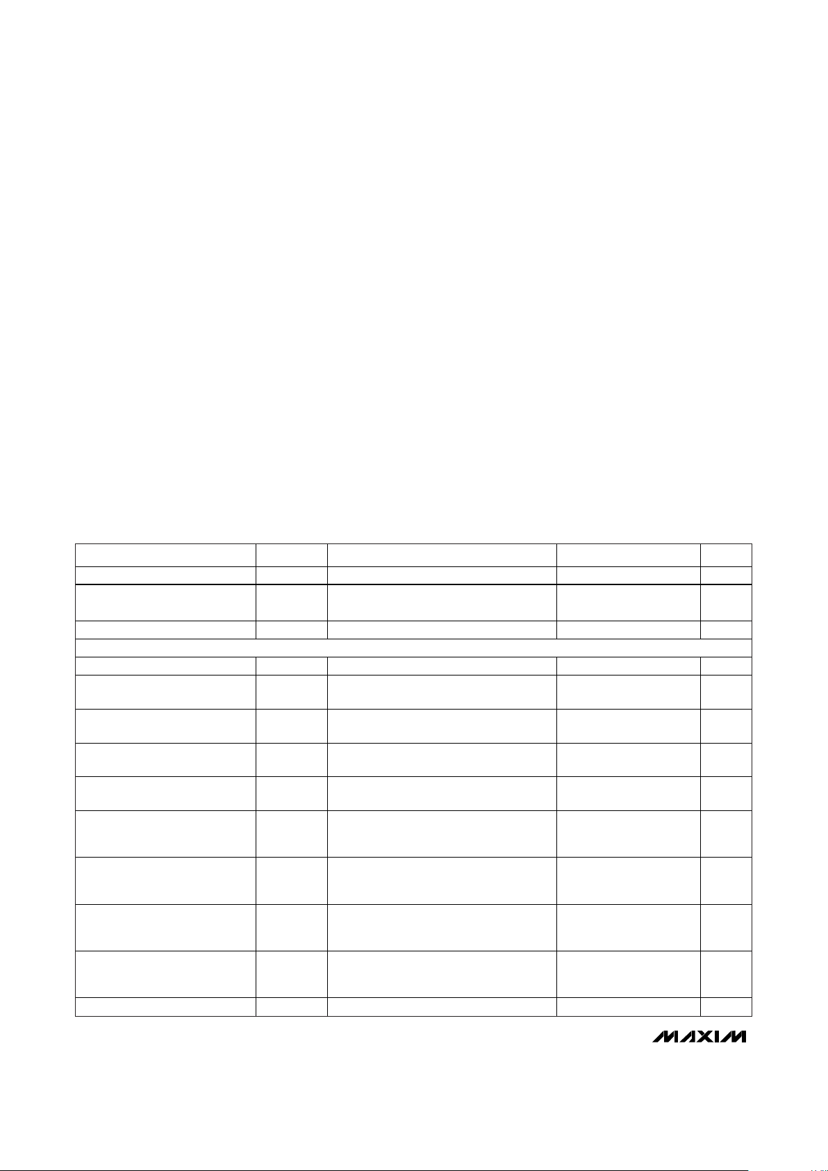
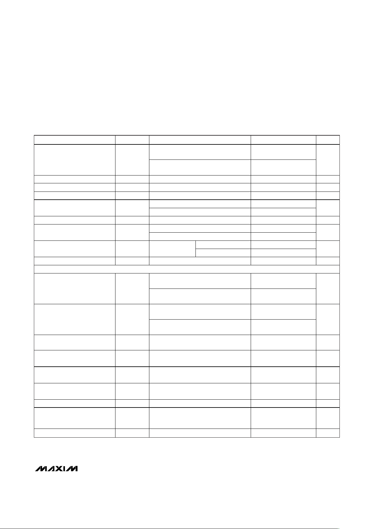
PARAMETER SYMBOL CONDITIONS MIN TYP MAX UNITS
Input Voltage Range UP/DN = LDO5, INLDO, INA = LDO5 5.5 38 V
INA Undervoltage Threshold V
INA(UVLO)
UP/DN = LDO5, INA = VCC, rising edge,
hysteresis = 160mV
4.0 4.2 4.4 V
INBC Input Voltage Range 2.3 5.5 V
SUPPLY CURRENTS
V
INLDO
Shutdown Supply Current I
IN(SHDN)VINLDO
= 5.5V to 38V, SHDN = GND 10 15 μA
V
INLDO
Suspend Supply Current I
IN(SUS)
V
INLDO
= 5.5V to 38V, ON_ = GND,
SHDN = INLDO
50 80 μA
VCC Shutdown Supply Current
SHDN = ONA = ONB = ONC = OND =
GND, T
A
= +25°C
0.1 1 μA
VDD Shutdown Supply Current
SHDN = ONA = ONB = ONC = OND =
GND, T
A
= +25°C
0.1 1 μA
INA Shutdown Current I
INA
SHDN = ONA = ONB = ONC = OND =
GND, UP/DN = V
CC
7 10 μA
VCC Supply Current
Main Step-Down Only
ONA = V
CC
, ONB = ONC = OND = GND;
does not include switching losses,
measured from V
CC
210 300 μA
VCC Supply Current
Main Step-Down and Reg ulator B
ONA = ONB = V
CC
, ONC = OND = GND;
does not include switching losses,
measured from V
CC
280 350 μA
VCC Supply Current
Main Step-Down and Reg ulator C
ONA = ONC = V
CC
, ONB = OND = GND;
does not include switching losses,
measured from V
CC
280 350 μA
VCC Supply Current
Main Step-Down and Reg ulator D
ONA = OND = V
CC
, ONB = ONC = GND;
does not include switching losses,
measured from V
CC
2.2 3 mA
INA Supply Current I
INA
ONA = VCC, UP/DN = VCC 40 60 μA
MAX17019
High-Input-Voltage Quad-Output Controller
_______________________________________________________________________________________ 3
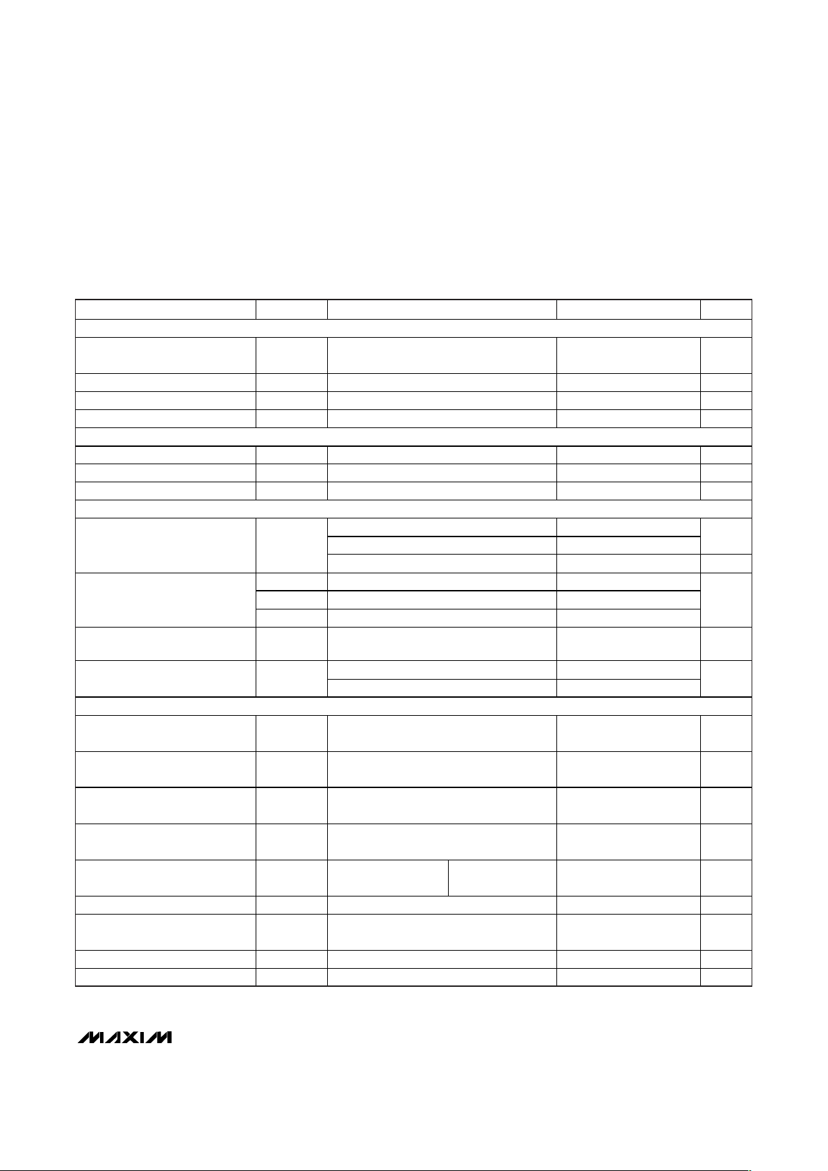
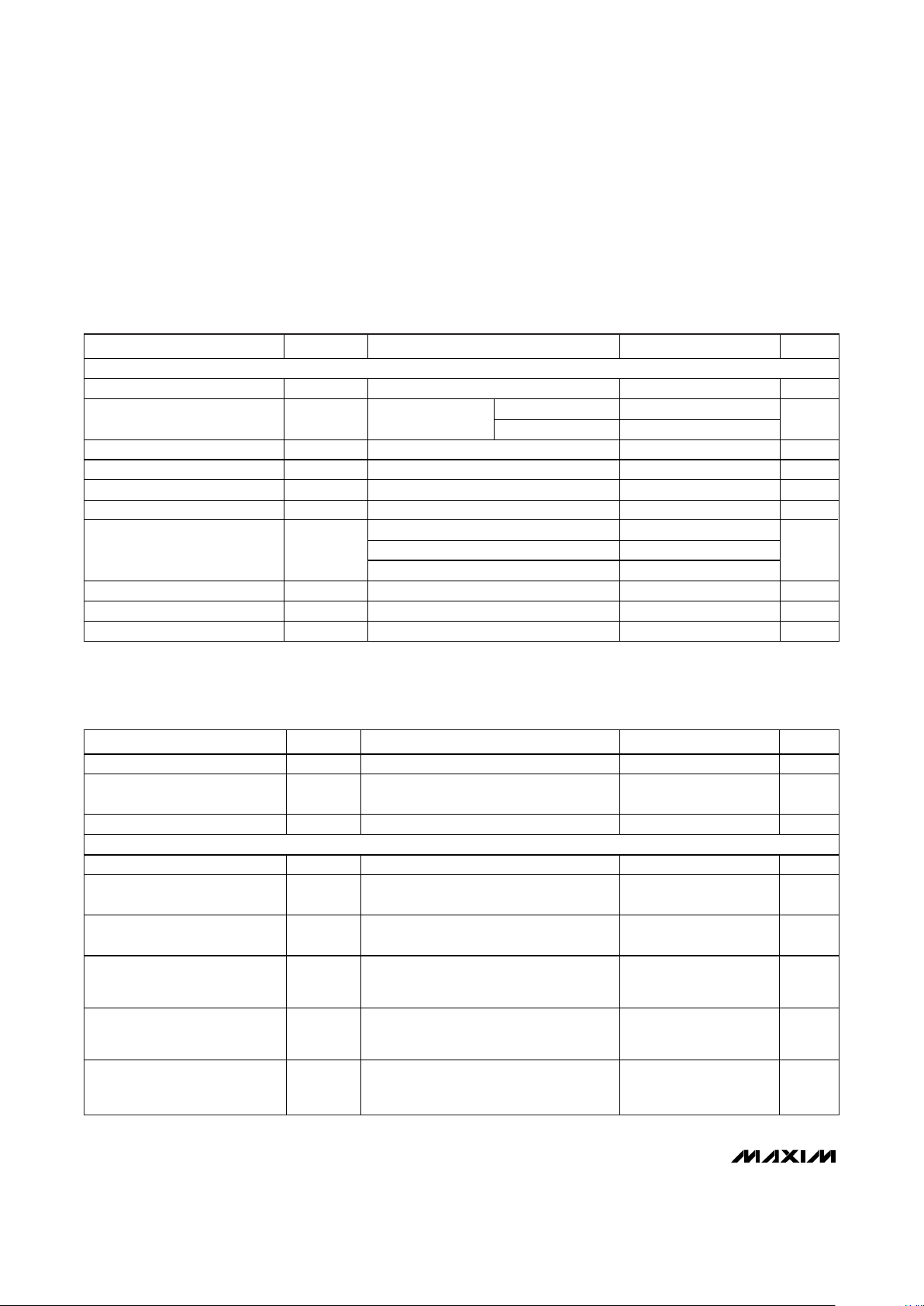
PARAMETER SYMBOL CONDITIONS MIN TYP MAX UNITS
5V LINEAR REGULATOR (LDO5)
LDO5 Output Voltage V
LDO5
V
INLDO
= 5.5V to 38V, I
LDO5
= 0 to 50mA,
BYP = GND
4.75 5.0 5.2 V
LDO5 Short-Circuit Current Limit LDO5 = BYP = GND, V
INLDO
= 5.5V 70 160 250 mA
BYP Switchover Threshold V
BYP
Rising edge 4.65 V
LDO5-to-BYP Switch Resistance R
BYP
LDO5 to BYP, V
BYP
= 5V, I
LDO5
= 50mA 1.5 4
1.25V REFERENCE
Reference Output Voltage V
REF
No load 1.237 1.25 1.263 V
Reference Load Regulation V
REF
I
REF
= -1μA to +50μA 3 10 mV
Reference Undervoltage Lockout V
REF(UVLO)
1.0 V
OSCILLATOR
FREQ = VCC 500
FREQ = REF 750
kHz
Oscillator Frequency f
OSC
FREQ = GND 0.9 1.0 1.1 MHz
f
SWA
Regulator A 1/2 f
OSC
f
SWB
Regulator B f
OSC
Switching Frequency
f
SWC
Regulator C 1/2 f
OSC
MHz
Maximum Duty Cycle
(All Switching Regulator s)
D
MAX
90 93.5 %
FREQ = VCC or GND 90
Minimum On-Time
(All Switching Regulator s)
t
ON(MIN)
FREQ = REF 75
ns
REGULATOR A (Main Step-Down)
Output Voltage-Adjust Range Step-down configuration (UP/DN = VCC) 1.0
V
CC
+
0.3
V
FBA Regulation Voltage V
FBA
Step-down configuration (UP/DN = VCC),
V
CSPA
- V
CSNA
= 0 to 20mV, 90% duty cycle
0.968 0.97 1.003 V
FBA Regulation Voltage
(Overload)
V
FBA
Step-down configuration (UP/DN = VCC),
V
CSPA
- V
CSNA
= 0 to 20mV, 90% duty cycle
0.930 1.003 V
FBA Load Regulation V
FBA
Step-down configuration (UP/DN = VCC),
V
CSPA
- V
CSNA
= 0 to 20mV
16 mV
FBA Line Regulation
UP/DN = V
CC
,
0 to 100% duty cycle
Step-down
(UP/DN = V
CC
)
10 16 22 mV
FBA Input Current I
FBA
UP/DN = GND or VCC, TA = +25°C -100 -5 +100 nA
Current-Sense Input CommonMode Range
V
CSA
0
V
CC
+
0.3V
V
Current-Sense Input Bias Current I
CSA
TA = +25°C 40 60 μA
Idle Mode™ Threshold V
IDLEA
4 mV
ELECTRICAL CHARACTERISTICS (continued)
(Circuit of Figure 1, V
INLDO
= 12V, V
INA
= V
INBC
= VDD= VCC= V
BYP
= V
CSPA
= V
CSNA
= 5V, V
IND
= 1.8V, V
SHDN
= V
ONA
= V
ONB
=
V
ONC
= V
OND
= 5V, I
REF
= I
LDO5
= I
OUTD
= no load, FREQ = GND, UP/DN = VCC, TA= 0°C to +85°C, unless otherwise noted.
Typical values are at T
A
= +25°C.) (Note 1)
Idle Mode is a trademark of Maxim Integrated Products, Inc.
MAX17019
High-Input-Voltage Quad-Output Controller
4 _______________________________________________________________________________________
ELECTRICAL CHARACTERISTICS (continued)
(Circuit of Figure 1, V
INLDO
= 12V, V
INA
= V
INBC
= VDD= VCC= V
BYP
= V
CSPA
= V
CSNA
= 5V, V
IND
= 1.8V, V
SHDN
= V
ONA
= V
ONB
=
V
ONC
= V
OND
= 5V, I
REF
= I
LDO5
= I
OUTD
= no load, FREQ = GND, UP/DN = VCC, TA= 0°C to +85°C, unless otherwise noted.
Typical values are at T
A
= +25°C.) (Note 1)
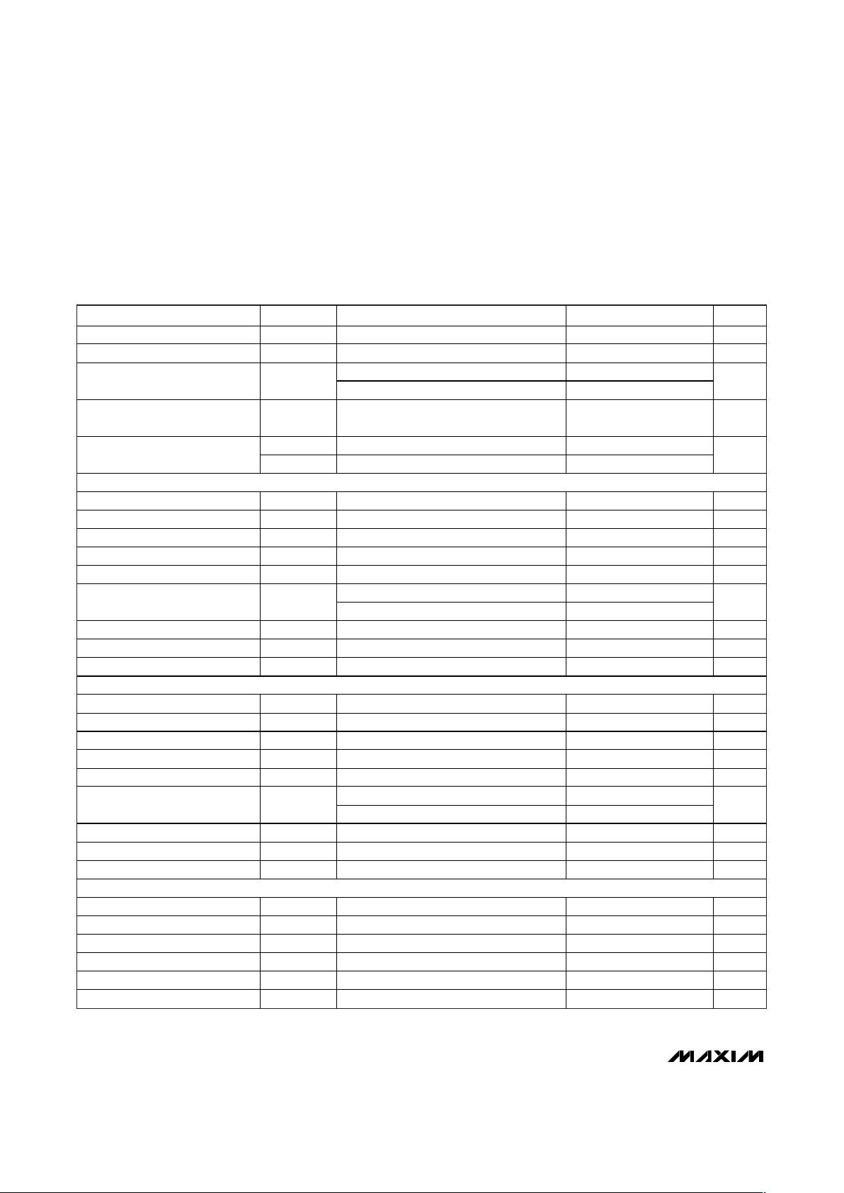
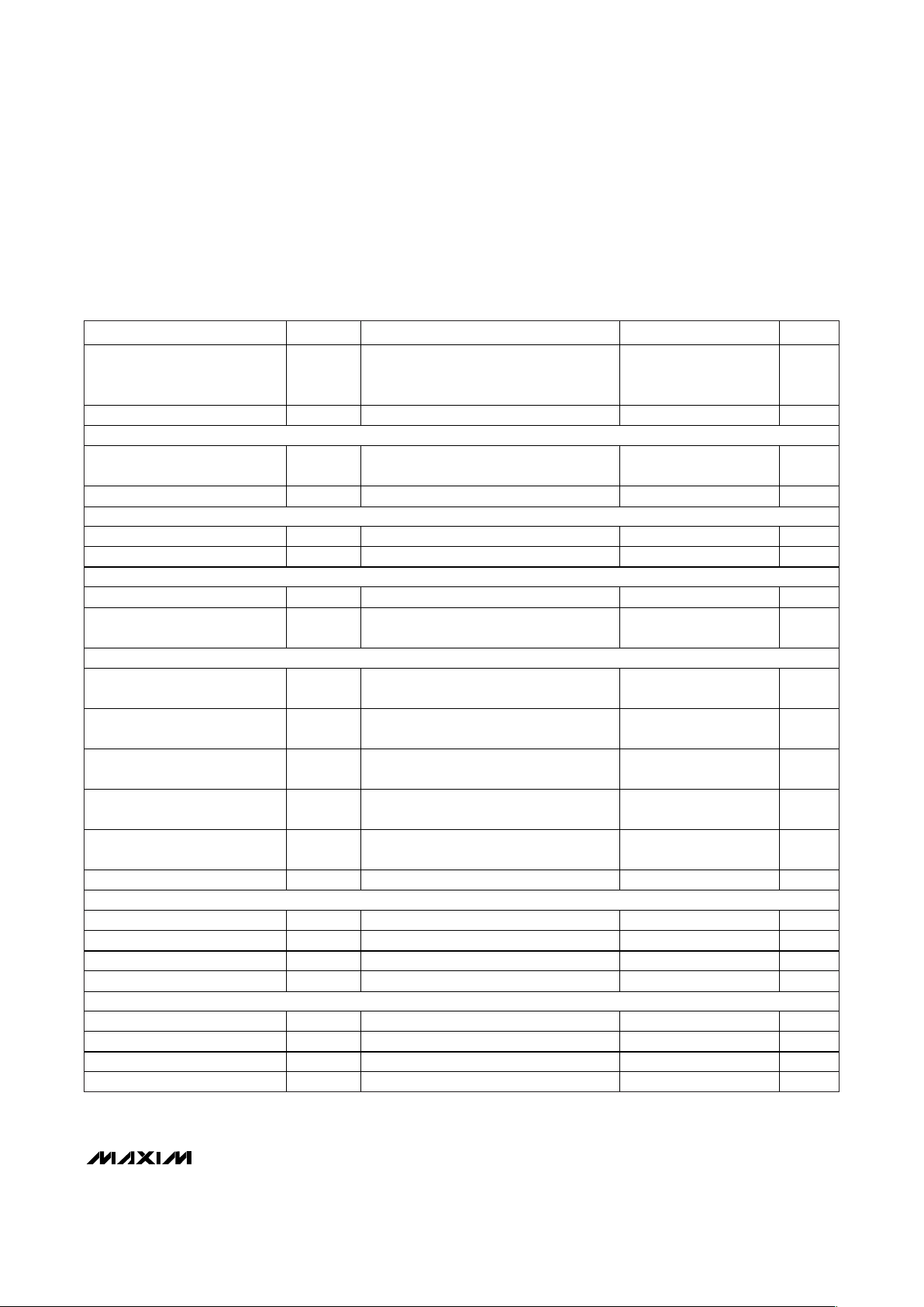
PARAMETER SYMBOL CONDITIONS MIN TYP MAX UNITS
Zero-Crossing Threshold V
IZX
1 mV
DHA Gate Driver On-Resistance R
DH
DHA forced high and low 2.5 5
DLA forced high 2.5 5
DLA Gate Driver On-Resistance R
DL
DLA forced low 1.5 3
DHA Gate Driver Source/Sink
Current
I
DH
DHA forced to 2.5V 0.7 A
I
DL(SRC)
DLA forced to 2.5V 0.7
DLA Gate Driver Source/Sink
Current
I
DL(SNK)
DLA forced to 2.5V 1.5
A
REGULATOR B (Internal 3A Step-Down Converter)
FBB Regulation Voltage I
LXB
= 0% duty cycle (Note 2) 0.747 0.755 0.762 V
FBB Regulation Voltage (Overload) V
FBB
I
LXB
= 0 to 2.5A, 0% duty cycle (Note 2) 0.720 0.762 V
FBB Load Regulation V
FBB
/I
LXB ILXB
= 0 to 2.5A -5 mV/A
FBB Line Regulation 0 to 100% duty cycle 7 8 10 mV
FBB Input Current I
FBB
TA = +25°C -100 -5 +100 nA
High-side n-channel 75 150
Internal MOSFET On-Resistance
Low-side n-channel 40 80
m
LXB Peak Current Limit I
PKB
3.0 3.45 4.0 A
LXB Idle-Mode Trip Level I
IDLEB
0.8 A
LXB Zero-Crossing Trip Level I
ZXB
100 mA
REGULATOR C (Internal 5A Step-Down Converter)
FBC Regulation Voltage I
LXC
= 0A, 0% duty cycle (Note 2) 0.747 0.755 0.762 V
FBC Regulation Voltage (Overload) V
FBC
I
LXC
= 0 to 4A, 0% duty cycle (Note 2) 0.710 0.762 V
FBC Load Regulation V
FBC
/I
LXC ILXC
= 0 to 4A -7 mV/A
FBC Line Regulation 0 to 100% duty cycle 12 14 16 mV
FBC Input Current I
FBC
TA = +25°C -100 -5 +100 nA
High-side n-channel 50 100
Internal MOSFET On-Resistance
Low-side n-channel 25 40
m
LXC Peak Current Limit I
PKC
5.0 5.75 6.5 A
LXC Idle-Mode Trip Level I
IDLEC
1.2 A
LXC Zero-Crossing Trip Level I
ZXC
100 mA
REGULATOR D (Source/Sink Linear Regulator and VTTR Buffer)
IND Input Voltage Range V
IND
1 2.8 V
IND Supply Current OND = VCC 10 50 μA
IND Shutdown Current OND = GND, TA = +25°C 10 μA
REFIND Input Range 0.5 1.5 V
REFIND Input Bias Current V
REFIND
= 0 to 1.5V, TA = +25°C -100 +100 nA
OUTD Output Voltage Range V
OUTD
0.5 1.5 V
MAX17019
High-Input-Voltage Quad-Output Controller
_______________________________________________________________________________________ 5
ELECTRICAL CHARACTERISTICS (continued)
(Circuit of Figure 1, V
INLDO
= 12V, V
INA
= V
INBC
= VDD= VCC= V
BYP
= V
CSPA
= V
CSNA
= 5V, V
IND
= 1.8V, V
SHDN
= V
ONA
= V
ONB
=
V
ONC
= V
OND
= 5V, I
REF
= I
LDO5
= I
OUTD
= no load, FREQ = GND, UP/DN = VCC, TA= 0°C to +85°C, unless otherwise noted.
Typical values are at T
A
= +25°C.) (Note 1)
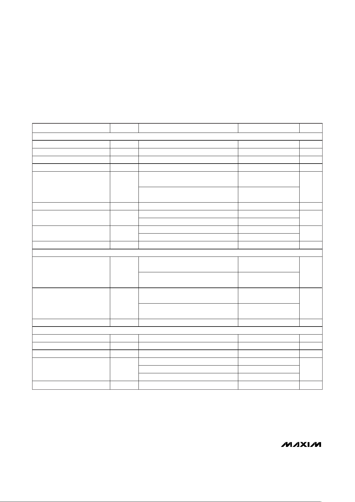
PARAMETER SYMBOL CONDITIONS MIN TYP MAX UNITS
V
FBD
with respect to V
REFIND
, OUTD =
FBD, I
OUTD
= +50μA (source load)
-10 0
FBD Output Accuracy V
FBD
V
FBD
with respect to V
REFIND
,
OUTD = FBD, I
OUTD
= -50μA (sink load)
0 +10
mV
FBD Load Regulation I
OUTD
= ±1A -17 -13 mV/A
FBD Line Regulation V
IND
= 1.0V to 2.8V, I
OUTD
= ±200mA 1 mV
FBD Input Current V
FBD
= 0 to 1.5V, TA = +25°C 0.1 0.5 μA
Source load +2 +4
OUTD Linear-Regulator Current
Limit
Sink load -2 -4
A
Current-Limit Soft-Start Time With respect to internal OND signal 160 μs
High-side on-resistance 120 250
Internal MOSFET On-Resistance
Low-side on-resistance 180 450
m
I
VTTR
= ±0.5mA -10 +10
VTTR Output Accuracy REFIND to VTTR
I
VTTR
= ±3mA -20 +20
mV
VTTR Maximum Current Rating ±5 mA
FAULT PROTECTION
Upper threshold rising edge,
hysteresis = 50mV
9 12 14
SMPS POK and Fault Thresholds
Lower threshold falling edge,
hysteresis = 50mV
-14 -12 -9
%
Upper threshold rising edge,
hysteresis = 50mV
6 12 16
VTT LDO POKD and Fault
Threshold
Lower threshold falling edge,
hysteresis = 50mV
-16 -12 -6
%
POK Propagation Delay t
POK
FB_ forced 50mV beyond POK_ trip
threshold
5 μs
Overvoltage Fault Latch Delay t
OVP
FB_ forced 50mV above POK_ upper
trip threshold
5 μs
SMPS Undervoltage Fault
Latch Delay
t
UVP
FBA, FBB, or FBC forced 50mV below
POK_ lower trip threshold
5 μs
VTT LDO Undervoltage Fault
Latch Delay
t
UVP
FBD forced 50mV below POKD lower
trip threshold
5000 μs
POK Output Low Voltage V
POK
I
SINK
= 3mA 0.4 V
POK Leakage Currents I
POK
V
FBA
= 1.05V, V
FBB
= V
FBC
= 0.8V, V
FBD
=
V
REFIND
+ 50mV (POK high impedance);
POK_ forced to 5V, T
A
= +25°C
1 μA
Thermal-Shutdown Threshold T
SHDN
Hysteresis = 15°C +160 °C
MAX17019
High-Input-Voltage Quad-Output Controller
6 _______________________________________________________________________________________
ELECTRICAL CHARACTERISTICS (continued)
(Circuit of Figure 1, V
INLDO
= 12V, V
INA
= V
INBC
= VDD= VCC= V
BYP
= V
CSPA
= V
CSNA
= 5V, V
IND
= 1.8V, V
SHDN
= V
ONA
= V
ONB
=
V
ONC
= V
OND
= 5V, I
REF
= I
LDO5
= I
OUTD
= no load, FREQ = GND, UP/DN = VCC, TA= 0°C to +85°C, unless otherwise noted.
Typical values are at T
A
= +25°C.) (Note 1)
PARAMETER SYMBOL CONDITIONS MIN TYP MAX UNITS
GENERAL LOGIC LEVELS
SHDN Input Logic Threshold Hysteresis = 20mV 0.5 1.6 V
SHDN = 0~16V -2 +2
SHDN Input Bias Current TA = +25°C
SHDN = 17V~38V -2 +150
μA
ON_ Input Logic Threshold Hysteresis = 170mV 0.5 1.6 V
ON_ Input Bias Current TA = +25°C -1 +1 μA
UP/DN Input Logic Threshold 0.5 1.6 V
UP/DN Input Bias Current TA = +25°C -1 +1 μA
High (VCC) VCC- 0.4V
Unconnected/REF 1.65 3.8
FREQ Input Voltage Levels
Low (GND) 0.5
V
FREQ Input Bias Current TA = +25°C -2 +2 μA
SYNC Input Logic Threshold 1.5 3.5 V
SYNC Input Bias Current TA = +25°C -1 +1 μA
ELECTRICAL CHARACTERISTICS
(Circuit of Figure 1, V
INLDO
= 12V, V
INA
= V
INBC
= VDD= VCC= V
BYP
= V
CSPA
= V
CSNA
= 5V, V
IND
= 1.8V, V
SHDN
= V
ONA
= V
ONB
=
V
ONC
= V
OND
= 5V, I
REF
= I
LDO5
= I
OUTD
= no load, FREQ = GND, UP/DN = VCC, TA= -40°C to +125°C.) (Note 1)
PARAMETER SYMBOL CONDITIONS MIN TYP MAX UNITS
Input Voltage Range UP/DN = LDO5, INLDO, INA = LDO5 5.5 24 V
INA Undervoltage Threshold V
INA(UVLO)
UP/DN = LDO5, INA = VCC, ris ing edge,
hysteresis = 160mV
3.9 4.5 V
INBC Input Voltage Range 2.3 5.5 V
SUPPLY CURRENTS
V
INLDO
Shutdown Supply Current I
IN(SHDN)VINLDO
= 5.5V to 38V, SHDN = GND 15 μA
V
INLDO
Suspend Supply Current I
IN(SUS)
V
INLDO
= 5.5V to 38V, ON_ = GND,
SHDN = INLDO
80 μA
INA Shutdown Current I
INA
SHDN = ONA = ONB = ONC = OND = GND,
UP/DN = V
CC
10 μA
VCC Supply C urrent
Main Step-Down Only
ONA = V
CC
, ONB = ONC = OND = GND;
does not include switching losses,
measured from V
CC
350 μA
VCC Supply Current
Main Step-Down and Regulator B
ONA = ONB = V
CC
, ONC = OND = GND;
does not include switching losses,
measured from V
CC
400 μA
VCC Supply Current
Main Step-Down and Regulator C
ONA = ONC = V
CC
, ONB = OND = GND,
does not include switching losses,
measured from V
CC
400 μA
MAX17019
High-Input-Voltage Quad-Output Controller
_______________________________________________________________________________________ 7
ELECTRICAL CHARACTERISTICS (continued)
(Circuit of Figure 1, V
INLDO
= 12V, V
INA
= V
INBC
= VDD= VCC= V
BYP
= V
CSPA
= V
CSNA
= 5V, V
IND
= 1.8V, V
SHDN
= V
ONA
= V
ONB
=
V
ONC
= V
OND
= 5V, I
REF
= I
LDO5
= I
OUTD
= no load, FREQ = GND, UP/DN = VCC, TA= -40°C to +125°C.) (Note 1)
PARAMETER SYMBOL CONDITIONS MIN TYP MAX UNITS
VCC Supply Current
Main Step-Down and Reg ulator D
ONA = OND = V
CC
, ONB = ONC = GND,
does not include switching losses,
measured from V
CC
3.5 mA
INA Supply Current (Step-Down) I
INA
ONA = VCC, UP/DN = VCC(step-down) 75 μA
5V LINEAR REGULATOR
LDO5 Output Voltage V
LDO5
V
INLDO
= 5.5V to 38V, I
LDO5
= 0 to 50mA,
BYP = GND
4.75 5.25 V
LDO5 Short-Circuit Current Limit LDO5 = BYP = GND, V
INLDO
= 5.5V 55 mA
1.25V REFERENCE
Reference Output Voltage V
REF
No load 1.237 1.263 V
Reference Load Regulation V
REF
I
REF
= -1μA to +50μA 12 mV
OSCILLATOR
Oscillator Frequency f
OSC
FREQ = GND 0.9 1.1 MHz
Maximum Duty Cycle
(All Switching Regulator s)
D
MAX
89 %
REGULATOR A (Main Step-Down)
Output Voltage Adjust Range Step-down configuration (UP/DN = VCC) 1.0
V
CC
+
0.3V
V
FBA Regulation Voltage
Step-down configuration,
V
CSPA
- V
CSNA
= 0mV, 90% duty cycle
0.963 1.008 V
FBA Regulation Voltage
(Overload)
V
FBA
Step-down configuration (UP/DN = VCC),
V
CSPA
- V
CSNA
= 0 to 20mV, 90% duty cycle
0.925 1.008 V
FBA Line Regulation Step-down (UP/DN = VCC) 10 33 mV
Current-Sense Input CommonMode Range
V
CSA
0
V
CC
+
0.3V
V
Current-Limit Threshold (Positive) V
ILIMA
17 23 mV
REGULATOR B (Internal 3A Step-Down Converter)
FBB Regulation Voltage I
LXB
= 0A, 0% duty cycle (Note 2) 0.742 0.766 V
FBB Regulation Voltage (Overload) V
FBB
I
LXB
= 0 to 2.5A , 0% duty cycle (Note 2) 0.715 0.766 V
FBB Line Regulation 6 12 mV
LXB Peak Current Limit I
PKB
2.7 4.2 A
REGULATOR C (Internal 5A Step-Down Converter)
FBC Regulation Voltage I
LXC
= 0A, 0% duty cycle (Note 2) 0.742 0.766 V
FBC Regulation Voltage (Overload) V
FBC
I
LXC
= 0 to 4A, 0% duty cycle (Note 2) 0.705 0.766 V
FBC Line Regulation 11 20 mV
LXC Peak Current Limit I
PKC
5.0 6.5 A
MAX17019
High-Input-Voltage Quad-Output Controller
8 _______________________________________________________________________________________
ELECTRICAL CHARACTERISTICS (continued)
(Circuit of Figure 1, V
INLDO
= 12V, V
INA
= V
INBC
= VDD= VCC= V
BYP
= V
CSPA
= V
CSNA
= 5V, V
IND
= 1.8V, V
SHDN
= V
ONA
= V
ONB
=
V
ONC
= V
OND
= 5V, I
REF
= I
LDO5
= I
OUTD
= no load, FREQ = GND, UP/DN = VCC, TA= -40°C to +125°C.) (Note 1)
PARAMETER SYMBOL CONDITIONS MIN TYP MAX UNITS
REGULATOR D (Source/Sink Linear Regulator and VTTR Buffer)
IND Input Voltage Range V
IND
1 2.8 V
IND Supply Current OND = VCC 70 μA
REFIND Input Range 0.5 1.5 V
OUTD Output Voltage Range V
OUTD
0.5 1.5 V
V
FBD
with respect to V
REFIND
,
OUTD = FBD, I
OUTD
= +50μA (source load)
-12 0
FBD Output Accuracy V
FBD
V
FBD
with respect to V
REFIND
,
OUTD = FBD, I
OUTD
= -50μA (sink load)
0 +12
mV
FBD Load Regulation I
OUTD
= ±1A -20 mV/A
Source load +2 +4
OUTD Linear-Regulator Current
Limit
Sink load -2 -4
A
High-side on-resistance 300
Internal MOSFET On-Resistance
Low-side on-resistance 475
m
VTTR Output Accuracy REFIND to VTTR, I
VTTR
= ±3mA -20 +20 mV
FAULT PROTECTION
Upper threshold rising edge,
hysteresis = 50mV
8 16
SMPS POK and Fault Thresholds
Lower threshold falling edge,
hysteresis = 50mV
-16 -8
%
Upper threshold rising edge,
hysteresis = 50mV
6 16
VTT LDO POKD and Fault
Threshold
Lower threshold falling edge,
hysteresis = 50mV
-16 -6
%
POK Output Low Voltage V
POK ISINK
= 3mA 0.4 V
GENERAL LOGIC LEVELS
SHDN Input Logic Threshold Hysteresis = 20mV 0.5 1.6 V
ON_ Input Logic Threshold Hysteresis = 170mV 0.5 1.6 V
UP/DN Input Logic Threshold 0.5 1.6 V
High (VCC) VCC- 0.4V
Unconnected/REF 1.65 3.8
FREQ Input Voltage Levels
Low (GND) 0.5
V
SYNC Input Logic Threshold 1.5 3.5 V
Note 1: Limits are 100% production tested at TA= +25°C. Maximum and minimum limits are guaranteed by design and
characterization.
Note 2: Regulation voltage tested with slope compensation. Typical value is equivalent to 0% duty cycle. In real applications, the
regulation voltage is higher due to the line regulation times the duty cycle.
 Loading...