

General Description
The MAX17005/MAX17006/MAX17015 are high-frequency multichemistry battery chargers. These circuits feature a new high-frequency current-mode architecture
that significantly reduces component size and cost*.
The charger uses a high-side MOSFET with n-channel
synchronous rectifier. Widely adjustable charge current,
charge voltage, and input current limit simplify the construction of highly accurate and efficient chargers.
The charge voltage and charge current are set with
analog control inputs. The charge current setting can
also be adjusted with a PWM input. High-accuracy current-sense amplifiers provide fast cycle-by-cycle current-mode control to protect against short circuits to the
battery and respond quickly to system load transients.
In addition, the charger provides a high-accuracy analog output that is proportional to the adapter current. In
the MAX17015, this current monitor remains active
when the adapter is absent to monitor battery discharge current.
The MAX17005 charges three or four Li+ series cells,
and the MAX17006 charges two or three Li+ series
cells. The MAX17015 adjusts the charge voltage setting
and the number of cells through a feedback resistordivider from the output. All variants of the charger can
provide at least 4A of charge current with a 10mΩ
sense resistor.
The charger utilizes a charge pump to control an n-channel
adapter selection switch. The charge pump remains
active even when the charger is off. When the adapter
is absent, a p-channel MOSFET selects the battery.
The MAX17005/MAX17006/MAX17015 are available in
a small, 4mm x 4mm x 0.8mm 20-pin, lead-free TQFN
package. An evaluation kit is available to reduce
design time.
Applications
Notebook Computers
Tablet PCs
Portable Equipment with Rechargeable Batteries
Features
♦ High Switching Frequency (1.2MHz)
♦ Controlled Inductor Current-Ripple Architecture
Reduced BOM Cost
Small Inductor and Output Capacitors
♦ ±0.4% Accurate Charge Voltage
♦ ±2.5% Accurate Input-Current Limiting
♦ ±3% Accurate Charge Current
♦ Single-Point Compensation
♦ Monitor Outputs for
±2.5% Accurate Input Current Limit
±2.5% Battery Discharge Current
(MAX17015 only)
AC Adapter Detection
♦ Analog/PWM Adjustable Charge-Current Setting
♦ Battery Voltage Adjustable for 3 and 4 Cells
(MAX17005) or 2 and 3 Cells (MAX17006)
♦ Adjustable Battery Voltage (4.2V to 4.4V/Cell)
♦ Cycle-by-Cycle Current Limit
Battery Short-Circuit Protection
Fast Response for Pulse Charging
Fast System-Load-Transient Response
♦ Programmable Charge Current < 5A
♦ Automatic System Power Source Selection with
n-Channel MOSFET
♦ Internal Boost Diode
♦ +8V to +26V Input Voltage Range
MAX17005/MAX17006/MAX17015
1.2MHz Low-Cost,
High-Performance Chargers
________________________________________________________________
Maxim Integrated Products
1
Ordering Information
19-4041; Rev 0; 2/08
For pricing, delivery, and ordering information, please contact Maxim Direct at 1-888-629-4642,
or visit Maxim’s website at www.maxim-ic.com.
EVALUATION KIT
AVAILABLE
+
Denotes a lead-free package.
Pin Configuration and Minimal Operating Circuit appear at
end of data sheet.
*
Patent pending.
PART TEMP RANGE
MAX17005ETP+ -40°C to +85°C
MAX17006ETP+ -40°C to +85° C
MAX17015ETP+ -40°C to +85° C
PINPACKAGE
20 Thin QFN
(4mm x 4mm)
20 Thin QFN
(4mm x 4mm)
20 Thin QFN
(4mm x 4mm)
PKG
CODE
T2044-3
T2044-3
T2044-3
MAX17005/MAX17006/MAX17015
1.2MHz Low-Cost,
High-Performance Chargers
2 _______________________________________________________________________________________
ABSOLUTE MAXIMUM RATINGS
ELECTRICAL CHARACTERISTICS
(Circuit of Figure 1, V
DCIN
= V
CSSP
= V
CSSN
= 19V, V
BATT
= V
CSIP
= V
CSIN
= 16.8V, V
VCTL
= VAA, V
ISET
= 1V, TA= 0°C to +85°C,
unless otherwise noted. Typical values are at T
A
= +25°C.)
Stresses beyond those listed under “Absolute Maximum Ratings” may cause permanent damage to the device. These are stress ratings only, and functional
operation of the device at these or any other conditions beyond those indicated in the operational sections of the specifications is not implied. Exposure to
absolute maximum rating conditions for extended periods may affect device reliability.
DCIN, CSSP, CSSN, BATT, CSIN, CSIP, ACOK,
LX to AGND .......................................................-0.3V to +30V
BST to LDO.............................................................-0.3V to +30V
CSIP to CSIN, CSSP to CSSN .............................. -0.3V to +0.3V
IINP, FB, ACIN to AGND.............................-0.3V to (V
AA
+ 0.3V)
V
AA
, LDO, ISET, VCTL, CC to AGND .......................-0.3V to +6V
DHI to LX ....................................................-0.3V to (BST + 0.3V)
BST to LX..................................................................-0.3V to +6V
DLO to PGND ............................................-0.3V to (LDO + 0.3V)
PGND to AGND .................................................... -0.3V to +0.3V
Continuous Power Dissipation (T
A
= +70°C)
16-Pin TQFN (derate 16.9mW/°C above +70°C)....1349.1mW
Operating Temperature Range ...........................-40°C to +85°C
Junction Temperature......................................................+150°C
Storage Temperature Range .............................-60°C to +150°C
Lead Temperature (soldering, 10s) .................................+300°C
CHARGE-VOLTAGE REGULATION
Battery Regulation-Voltage Accuracy
FB Input Bias Curent -1 +1 μA
VCTL Range
VCTL Gain V
VCTL Input Bias Current V
CHARGE-CURRENT REGULATION
ISET Range 0.0 VAA/2 V
ISET Full-Scale Setting
Ful l-Charge Current Accuracy
(CSIP to CSIN)
Trickle Charge-Current Accuracy
Charge-Current Gain Error Based on V
Charge-Current Offset Error Based on V
BATT/CSIP/CSIN Input Voltage Range 0 24 V
ISET Power-Down Mode Threshold
PARAMETER CONDITIONS MIN TYP MAX UNITS
2 cel ls, V
3 cel l s, V
4 cel ls, V
FB accuracy using FB divider (for MAX17015)
(Note 1)
2 cells (for MAX17006), 4 cell s (for MAX17005) 0.0
3 cell s (for MAX17005 and MAX17006)
CELL/VVCTL
VCTL
ISET = 1.4V 80
ISET = 99.9% duty cycle 60
V
BATT
ISET falling 21 26 31
ISET ri sing 33 40 47
VCTL
= VAA(for MAX17005 and MAX17006) 12.549 12.60 12.651
VCTL
VCTL
5.85 6 6.15 V/V
= GND and VCTL = V
= 1V to 16.8V
ISET
ISET
= GND (for MAX17006) 8.3664 8.40 8.4336
= GND (for MAX17005) 16.733 16.80 16.867
= V
VAA
= V
VAA
AA
V
= VAA/4 or ISET
ISET
= 99.9% duty cycle
V
= VAA/6 or ISET
ISET
= 66.7% duty cycle
V
= VAA/80 or ISET
ISET
= 5% duty cycle
/4 and V
/4 and V
ISET
ISET
= V
= V
/80 -2 +2 %
VAA
/80 -1.4 +1.4 mV
VAA
2.0916 2.1 2.1084
V
AA
-0.2
VAA/2
+0.2
-1 +1 μA
58.2 60 61.8 mV
-3 +3 %
38.2 40 41.8 mV
-4.5 +4.5 %
1.4 3 4.6 mV
-52 +52 %
V
AA
/2
V
V
mV
mV
MAX17005/MAX17006/MAX17015
1.2MHz Low-Cost,
High-Performance Chargers
_______________________________________________________________________________________ 3
ELECTRICAL CHARACTERISTICS (continued)
(Circuit of Figure 1, V
DCIN
= V
CSSP
= V
CSSN
= 19V, V
BATT
= V
CSIP
= V
CSIN
= 16.8V, V
VCTL
= VAA, V
ISET
= 1V, TA= 0°C to +85°C,
unless otherwise noted. Typical values are at T
A
= +25°C.)
PARAMETER CONDITIONS MIN TYP MAX UNITS
ISET Input Bias Current
ISET PWM Threshold
ISET Frequency 0.128 500 kHz
ISET Effective Resolution f
INPUT-CURRENT REGULATION
Input Current-Limit Threshold V
CSSN Input Bias Current Adapter present -0.1 +0.1 μA
CSSP/CSSN Input-Voltage Range 8.0 26.0 V
IINP Transconductance V
IINP Accuracy
SUPPLY AND LINEAR REGULATOR
DCIN Input Voltage Range 8 26 V
DCIN Undervoltage-Lockout (UVLO) Trip-Point
DCIN + CSSP + CSSN Quiescent Current
BATT + CSIP + CSIN + LX Input Current
LDO Output Voltage 8.0V < V
LDO Load Regulation 0 < I
LDO UVLO Threshold 3.2 4.1 5.0 V
REFERENCES
VAA Output Voltage I
VAA UVLO Threshold VAA falling 3.1 3.9 V
ACIN
ACIN Thresho ld 2.058 2.1 2.142 V
ACIN Threshold Hysteresis 10 20 30 mV
ACIN Input Bias Current -1 +1 μA
ACOK
ACOK Sink Current V
ACOK Leakage Current V
V
ISET
CSSN = BATT, V
Ri sing 2.4
Fal ling 0.8
PWM
CSSP
CSSP
V
CSSP
V
CSSP
DCIN falling 7.9 8.1
DCIN rising 8.7 8.9
Adapter present (Note 2) 3 6 mA
Adapter absent (Note 2) 30 50 μA
V
BATT
V
BATT
VAA
ACOK
ACOK
= 3V -0.2 +0.2
=3.2MHz 8 Bits
- V
CSSN
- V
CSSN
- V
CSSN
- V
CSSN
= 16.8V
= 2V to 19V, adapter present (Note 2) 200 500
DCIN
< 40mA 100 200 mV
LDO
= 50μA 4.18 4.20 4.22 V
= 0.4V, V
= 5.5V, V
ISET
= 60mV 2.66 2.8 2.94 μA/mV
= 60mV, V
= 35mV -2.5 +2.5
< 26V, no load 5.15 5.35 5.55 V
ACIN
ACIN
= 5V -0.2 +0.2
= 0V to 4.5V -2.5 +2.5
IINP
Adapter absent (Note 2) 10 20
Charger shutdown (Note 2) 10 20
= 1.5V 6 mA
= 2.5V 1 μA
58.5 60 61.5 mV
-2.5 +2.5 %
μA
V
%
V
μA
MAX17005/MAX17006/MAX17015
1.2MHz Low-Cost,
High-Performance Chargers
4 _______________________________________________________________________________________
ELECTRICAL CHARACTERISTICS (continued)
(Circuit of Figure 1, V
DCIN
= V
CSSP
= V
CSSN
= 19V, V
BATT
= V
CSIP
= V
CSIN
= 16.8V, V
VCTL
= VAA, V
ISET
= 1V, TA= 0°C to +85°C,
unless otherwise noted. Typical values are at T
A
= +25°C.)
ELECTRICAL CHARACTERISTICS
(Circuit of Figure 1, V
DCIN
= V
CSSP
= V
CSSN
= 19V, V
BATT
= V
CSIP
= V
CSIN
= 16.8V, V
VCTL
= VAA, V
ISET
= 1V, TA= -40°C to +85°C,
unless otherwise noted.)
PARAMETER CONDITIONS MIN TY P MAX UNITS
SWITCHING REGULATOR
DHI Off-Time K Factor V
Sense Voltage for Minimum Discontinuous
Mode Ripple Current
Zero-Cros sing Comparator Threshold V
Cycle-by-Cycle Current-Limit Sense Voltage V
DHI Resistance High I
DHI Resistance Low I
DLO Resistance High I
DLO Resistance Low I
ADAPTER DETECTION
Adapter Absence-Detect Threshold V
Adapter Detect Threshold V
Adapter Switch Charge-Pump Frequency Charger Shutdown 180 200 220 Hz
Adapter Switch Charge-Pump Refresh Pulse
DCIN
V
CSIP
CSIP
CSIP
DLO
DLO
DLO
DLO
DCIN
DCIN
= 19V, V
- V
CSIN
- V
CSIN
- V
CSIN
BATT
= 10V 0.029 0.030 0.041 μs/V
10 mV
10 mV
105 110 115 mV
=10mA 1.5 3
= -10mA 0.8 1.75
= 10mA 3 6
= -10mA 3 7
- V
, V
BATT
- V
BATT,VDCIN
falling +70 +120 +170 mV
DCIN
rising +360 +420 +580 mV
DLO 0.04 0.1 0.20
DHI 0.07 0.15 0.30
μs
PARAMETER CONDITIONS MIN TY P MAX UNITS
CHARGE-VOLTAGE REGULATION
Battery Regulation-Voltage Accuracy
VCTL Range
VCTL Gain V
2 cel ls, V
3 cel ls, V
VCTL
VCTL
= GND (for MAX17006) 8.366 8.433
= V
AA
(for MAX17005 and MAX17006)
4 cel ls, V
= GND (for MAX17005) 16.73 16.86
VCTL
FB accuracy using FB divider (for MAX17015)
(Note 1)
2 cel ls (for MAX17006),
4 cell s (for MAX17005)
3 cell s (for MAX17005 and MAX17006)
CELL/VVCTL
5.85 6.15 V/V
12.549 12.651
2.091 2.108
VAA/2
+ 0.2
0.0
VAA/2
- 0.2
V
AA
V
V
MAX17005/MAX17006/MAX17015
1.2MHz Low-Cost,
High-Performance Chargers
_______________________________________________________________________________________ 5
ELECTRICAL CHARACTERISTICS (continued)
(Circuit of Figure 1, V
DCIN
= V
CSSP
= V
CSSN
= 19V, V
BATT
= V
CSIP
= V
CSIN
= 16.8V, V
VCTL
= VAA, V
ISET
= 1V, TA= -40°C to +85°C,
unless otherwise noted.)
PARAMETER CONDITIONS MIN TYP MAX UNITS
CHARGE-CURRENT REGULATION
ISET Range 0.0 VAA/2 V
Ful l Charge-Current Accurac y
(CSIP to CSIN)
Trickle Charge-Current Accuracy
Charge-Current Gain Error Based on V
Charge-Current Offset Error Based on V
BATT/CSIP/CSIN Input Voltage Range 0 24 V
ISET Power-Down Mode Threshold
ISET PWM Threshold
ISET Frequency 0.128 500 kHz
INPUT-CURRENT REGULATION
Input Current-Limit Threshold V
CSSN Input Bias Current Adapter present -2 +2 μA
CSSP/CSSN Input-Voltage Range 8.0 26.0 V
IINP Transconductance V
IINP Accuracy
SUPPLY AND LINEAR REGULATOR
DCIN Input-Voltage Range 8 26 V
DCIN UVLO Trip-Point
DCIN + CSSP + CSSN Quiescent Current
BATT + CSIP + CSIN + LX Input Current
LDO Output Voltage 8.0V < V
LDO Load Regulation 0 < I
LDO UVLO Threshold 3.2 5.0 V
V
= 1V to 16.8V
BATT
ISET
ISET
V
ISET
= VAA/4 or
ISET = 99.9% duty cycl e
V
= VAA/6 or
ISET
ISET = 66.7% duty cycl e
V
= VAA/80 or
ISET
ISET = 5% duty cycle
= V
/4 and V
= V
VAA
VAA
/4 and V
ISET
ISET
57.5 62.5 mV
-4.2 +4.2 %
38 42 mV
-5 +5 %
1.4 4.6 mV
-52 +52 %
= V
/80 -2 +2 %
VAA
= V
/80 -1.4 +1.4 mV
VAA
ISET falling 21 31
ISET ris ing 33 47
Ri sing 2.4
Fal ling 0.8
CSSP
CSSP
V
CSSP
V
CSSP
- V
- V
- V
- V
CSSN
= 60mV 2.66 2.94 μA/mV
CSSN
= 60mV, V
CSSN
= 35mV -2.5 +2.5
CSSN
= 0V to 4.5V -2.5 +2.5
IINP
58.2 61.8 mV
-3 +3 %
DCIN falling 7.9
DCIN rising 8.9
Adapter present (Note 2) 6 mA
Adapter absent (Note 2) 50 μA
V
= 16.8V
BATT
V
= 2V to 19V, adapter present (Note 2) 500
BATT
DCIN
< 40mA 200 mV
LDO
Adapter absent (Note 2) 20
Charger shutdown (Note 2) 20
< 26V, no load 5.15 5.55 V
mV
V
%
V
μA
MAX17005/MAX17006/MAX17015
1.2MHz Low-Cost,
High-Performance Chargers
6 _______________________________________________________________________________________
ELECTRICAL CHARACTERISTICS (continued)
(Circuit of Figure 1, V
DCIN
= V
CSSP
= V
CSSN
= 19V, V
BATT
= V
CSIP
= V
CSIN
= 16.8V, V
VCTL
= VAA, V
ISET
= 1V, TA= -40°C to +85°C,
unless otherwise noted.)
Note 1: Accuracy does not include errors due to external resistance tolerances.
Note 2: Adapter present conditions are tested at V
DCIN
= 19V and V
BATT
= 16.8V. Adapter absent conditions are tested at
V
DCIN
= 16V, V
BATT
= 16.8V.
PARAMETER CONDITIONS MIN TY P MAX UNITS
REFERENCES
VAA Output Voltage I
VAA UVLO Threshold VAA falling 3.9 V
ACIN
ACIN Thresho ld 2.058 2.142 V
ACIN Threshold Hysteresis 10 30 mV
ACOK
ACOK Sink Current V
SWITCHING REGULATOR
DHI Off-Time K Factor V
Cycle-by-Cycle Current-Limit Sense Voltage V
DHI Resistance High I
DHI Resistance Low I
DLO Resistance High I
DLO Resistance Low I
ADAPTER DETECTION
Adapter Absence-Detect Threshold V
Adapter Detect Threshold V
Adapter Switch Charge-Pump Frequency 180 220 Hz
Adapter Switch Charge-Pump Refresh Pulse
VAA
DLO
DLO
DLO
DLO
DLO 0.04 0.2
DHI 0.07 0.3
= 50μA 4.18 4.22 V
= 0.4V, V
ACOK
= 19V, V
DCIN
- V
CSIP
CSIN
= 10mA 3
= -10mA 1.75
= 10mA 6
= -10mA 7
- V
DCIN
BATT
- V
DCIN
BATT,VDCIN
, V
ACIN
BATT
DCIN
= 1.5V 6 mA
= 10V 0.029 0.041 μs/V
falling +70 +170 mV
rising +320 +620 mV
105 115 mV
μs
MAX17005/MAX17006/MAX17015
1.2MHz Low-Cost,
High-Performance Chargers
_______________________________________________________________________________________ 7
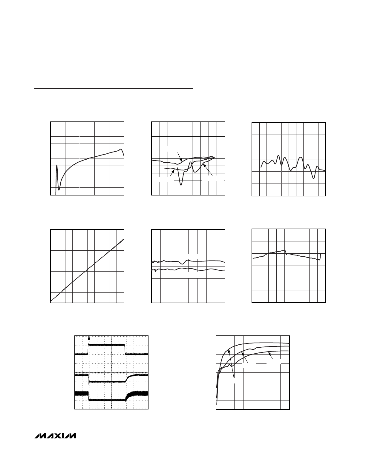
Typical Operating Characteristics
(Circuit of Figure 1, adapter = 19V, battery = 10V, ISET = 1.05V, V
CTL
= GND, TA= +25°C, unless otherwise noted.)
IINP DC ERROR
vs. SYSTEM CURRENT
MAX17005 toc01
SYSTEM CURRENT (A)
IINP ERROR (%)
4312
-8
-6
-4
-2
0
2
4
6
8
10
-10
05
IINP ERROR
vs. SYSTEM CURRENT
MAX17005 toc02
SYSTEM CURRENT (A)
IINP ERROR (%)
4.03.52.5 3.01.0 1.5 2.00.5
-8
-6
-4
-2
0
2
4
6
8
10
-10
04.5
V
BATT
= 16.8V
V
BATT
= 8.4V
V
BATT
= 12.6V
ISET PWM DUTY-CYCLE CHANGE
MAX17005 toc03
DUTY CYCLE
CHARGE-CURRENT ERROR (%)
0.8 0.90.1 0.2 0.3 0.4 0.5 0.6 0.7
0.5
1.0
1.5
2.0
2.5
3.0
0
01.0
ISET PWM DUTY-CYCLE CHANGE
MAX17005 toc04
DUTY CYCLE
CHARGE CURRENT (A)
80 9010 20 30 40 50 60 70
0.5
1.0
1.5
2.0
2.5
3.0
3.5
0
0100
ISET PWM FREQUENCY SWEEP
MAX17005 toc05
FREQUENCY (kHz)
CHARGE-CURRENT ERROR (%)
600 700100 200 300 400 500
0.5
1.0
1.5
2.0
2.5
3.0
0
0 800
DUTY CYCLE = 75%
DUTY CYCLE = 25%
BATTERY VOLTAGE-SETTING ERROR
MAX17005 toc06
VCTL (V)
BATTERY VOLTAGE ERROR (%)
3.0 3.5 4.00.5 1.0 1.5 2.0 2.5
-0.5
-0.4
-0.3
-0.2
-0.1
0
-0.6
04.5
SYSTEM LOAD TRANSIENT
MAX17005 toc07
200μs/div
SYSTEM
CURRENT
5A/div
CHARGING
CURRENT
5A/div
INDUCTOR
CURRENT
5A/div
EFFICIENCY
vs. CHARGE CURRENT
MAX17005 toc08
CHARGE CURRENT (A)
EFFICIENCY (%)
2.5 3.0 3.50.5 1.0 1.5 2.0
70
65
75
80
85
95
90
100
60
04.0
2 CELLS
3 CELLS
4 CELLS
VAA LOAD REGULATION
MAX17005 toc11
LOAD CURRENT (mA)
V
AA
VOLTAGE (V)
0.80.2 0.4 0.6
4.197
4.196
4.198
4.200
4.199
4.201
4.203
4.202
4.205
4.204
4.195
01.0
MAX17005/MAX17006/MAX17015
1.2MHz Low-Cost,
High-Performance Chargers
8 _______________________________________________________________________________________
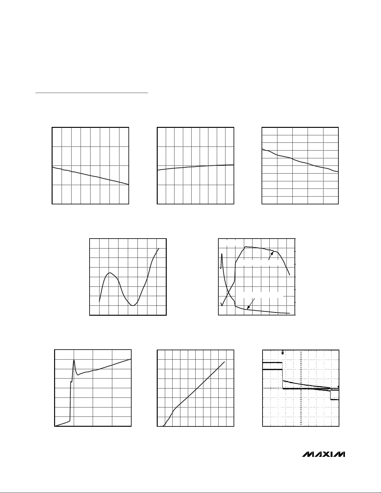
Typical Operating Characteristics (continued)
(Circuit of Figure 1, adapter = 19V, battery = 10V, ISET = 1.05V, V
CTL
= GND, TA= +25°C, unless otherwise noted.)
5.50
5.45
5.40
LDO VOLTAGE (V)
5.35
5.30
040
LDO CURRENT (mA)
3551015202530
MAX17005 toc09
5.50
5.45
5.40
LDO VOLTAGE (V)
5.35
5.30
LDO LOAD REGULATION
LDO LINE REGULATION
826
INPUT VOLTAGE (V)
242210 12 14 16 18 20
HIGH-SIDE MOSFET OFF-TIME AND
4.2005
VAA vs. TEMPERATURE
4.2000
4.1995
4.1990
(V)
4.1985
AA
V
4.1980
4.1975
4.1970
4.1965
-60 100
TEMPERATURE (°C)
60 80-40 -20 0 20 40
MAX17005 toc12
SWITCHING FREQUENCY vs. BATTERY VOLTAGE
1.6 6
VIN = 20V
1.4
1.2
1.0
0.8
0.6
0.4
SWITCHING FREQUENCY (MHz)
0.2
0
HIGH-SIDE MOSFET OFF-TIME
018
MAX17005 toc10
SWITCHING FREQUENCY
BATTERY VOLTAGE (V)
MAX17005 toc13
161410 124682
5
4
3
2
HIGH-SIDE MOSFTE OFF-TIME (μs)
1
0
ADAPTER CURRENT
vs. ADAPTER VOLTAGE
1.6
1.4
1.2
1.0
0.8
0.6
ADAPTER CURRENT (mA)
0.4
0.2
0
020
ADAPTER VOLTAGE (V)
15510
MAX17005 toc14
400
BATTERY LEAKAGE
350
300
250
200
150
100
BATTERY LEAKAGE CURRENT (μA)
50
0
020
BATTERY VOLTAGE (V)
14 16 18682 4 10 12
MAX17005 toc15
ADAPTER REMOVAL
200ms/div
MAX17005 toc16
5.00V
5.00V
5.00V

MAX17005/MAX17006/MAX17015
1.2MHz Low-Cost,
High-Performance Chargers
_______________________________________________________________________________________ 9
Pin Description
Dual Mode is a trademark of Maxim Integrated Products, Inc.
PIN NAME FUNCTION
1 DCIN Charger Bia s Suppl y Input. B ypass DCIN with a 1μF capacitor to PGND.
2 AGND Analog Ground
3 CSIP Output Current-Sense Pos it ive Input. Connect a current-sense resistor from CSIP to CSIN.
4 CSIN Output Current-Sense Negative Input
Input Current-Monitor Output. IINP sources the current proportional to the current sen sed across
5 IINP
6 BATT Battery Voltage Feedback Input
7 ACOK
8 CSSP Input Current Sense for Positive I nput. C onnect a current- sense re sist or from CSSP to CSSN.
9 CSSN Input Current-Sense Negative Input
10 ISET
11 PGND Power Ground Connection for MOSFET Drivers
12 DLO Low-Side Power-MOSFET Driver Output. Connect to low-side n-channel MOSFET gate.
13 LDO
14 BST High-Side Driver Supply. Connect a 0.68μF capac itor from BST to LX.
15 DHI High-Side Power-MOSFET Driver Output. Connect to high-side n-channel MOSFET gate.
16 LX High-Side Dri ver Source Connection. Connect a 0.68μF capacitor from BST to LX.
17 ACIN AC Adapter Detect Input. ACIN is the input to an uncommitted comparator.
18 V
19 CC
20 VCTL
— BP Backside Paddle. Connect the backside paddle to analog ground.
AA
CSSP and CSSN. The transconductance from (CSSP - CSSN) to IINP is 2.8μA/ mV. See the Analog
Input Current-Monitor Output section to configure the current mon itor for a particu lar gain setting.
AC Detect Output. Thi s open-drain output is high impedance when ACIN is lower than V
Connect a 10k pul lup resistor from LDO to ACOK.
Dual Mode™ Input for Setting Maximum Charge Current. ISET can be conf igured either with a
resi stor vo ltage-divider or with a PWM signal from 128Hz to 500 kHz. If there is no clock edge
within 20ms, ISET defaults to analog input mode. Pull ISET to GND to shut down the charger.
In the MAX17015, when the adapter is ab sent, drive ISET above 1V to enable IINP during battery
discharge. When the adapter is reinserted, ISET must be released to the correct control level within
300m s.
Linear Regulator Output. LDO provides the power to the MOSFET drivers. LDO is the output of the 5.4V
linear regulator supplied from DCIN. Bypas s LDO with a 4.7μF ceramic capacitor from LDO to PGND.
4.2V Voltage Reference and Device Power-Supply Input. Bypa ss VAA with a 1μF capacitor to GND.
Voltage Regulation Loop-Compensation Point. Connect 3k and 0.01μF capacitor in serie s from
CC to GND.
Battery Voltage Adjust Input. VCTL sets the number of cell s and adjusts the vo ltage per cell. The
adjustment range is 4.2V to 4.4V per cel l. See the Setting Charge Voltage section.
AA
/2.
MAX17005/MAX17006/MAX17015
1.2MHz Low-Cost,
High-Performance Chargers
10 ______________________________________________________________________________________
Figure 1. Typical Operating Circuit
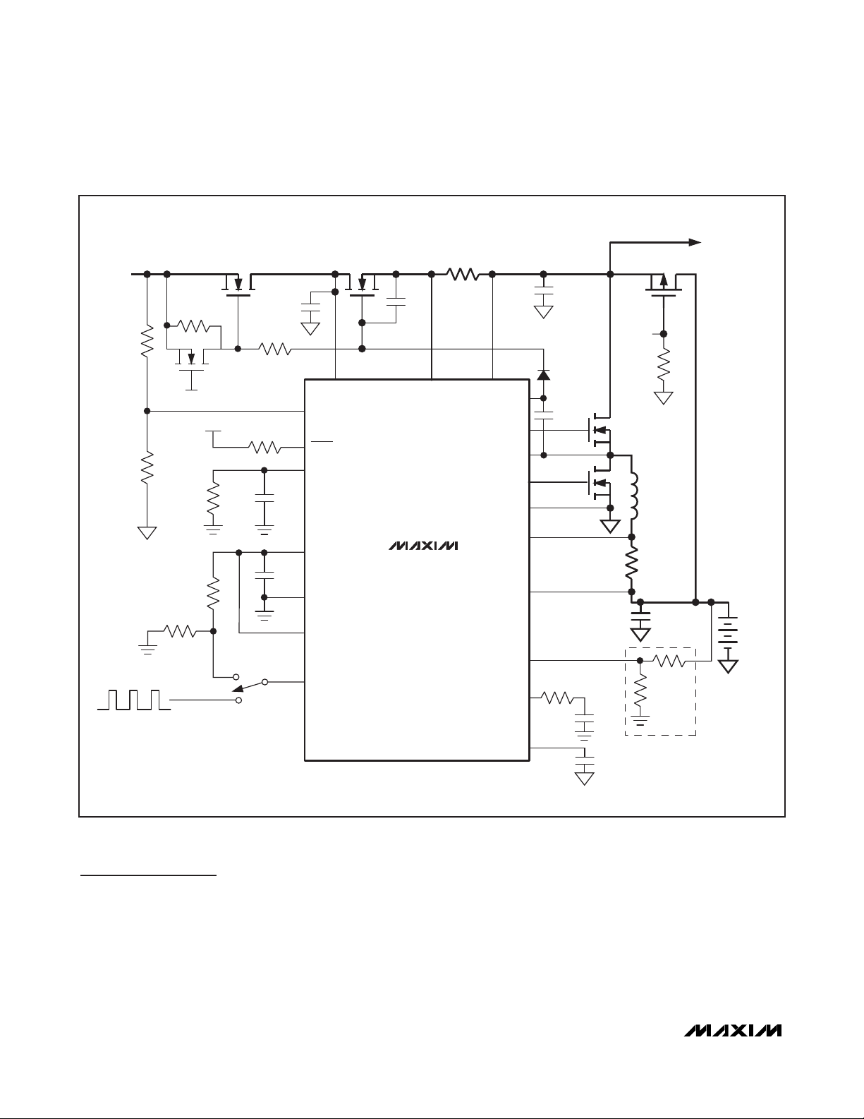
Detailed Description
The MAX17005/MAX17006/MAX17015 include all the
functions necessary to charge Li+, NiMH, and NiCd
batteries. An all n-channel synchronous-rectified stepdown DC-DC converter is used to implement a precision constant-current, constant-voltage charger. The
charge current and input current-limit sense amplifiers
have low-input offset errors (250μV typ), allowing the
use of small-valued sense resistors.
The MAX17005/MAX17006/MAX17015 use a new thermally optimized high-frequency architecture. With this
new architecture, the switching frequency is adjusted
to control the power dissipation in the high-side
MOSFET. Benefits of the new architecture include:
reduced output capacitance and inductance, resulting in
smaller printed-circuit board (PCB) area and lower cost.
RS1
ADAPTER
R
R
ACIN1
ACIN2
N4
R9
2MΩ
BATT
22.6kΩ
R3
Q1a
N3
C6
1μF
R4
200kΩ
DCIN
C2
0.1μF
C3
1μF
ACIN
ACOK
IINP
V
AA
GND
VCTL
LDO
R1
R2
10kΩ
C7
0.1μF
MAX17005
MAX17006
MAX17015
15mΩ
CSSP CSSN
BST
DHI
DLO
PGND
CSIP
CSIN
SYSTEM LOAD
Q1b
C
IN
ADAPTER
R6
N2
N1
200kΩ
C
C
L1 = 2μH
= 2 x 4.7μF
IN
= 4.7μF
OUT
L1
RS2
10mΩ
C
OUT
BATTERY
D1
C4
0.68μF
LX
BATT
PWM SIGNAL
ISET
LDO
R5
3kΩ
CC
C5
0.01μF
C1
4.7μF
R7
R8
ONLY FOR MAX17015

MAX17005/MAX17006/MAX17015
1.2MHz Low-Cost,
High-Performance Chargers
______________________________________________________________________________________ 11
Figure 2. Functional Diagram
The MAX17005/MAX17006/MAX17015 feature a voltage-regulation loop (CCV) and two current-regulation
loops (CCI and CCS). The loops operate independently
of each other. The CCV voltage-regulation loop monitors BATT to ensure that its voltage never exceeds the
voltage set by VCTL. The CCI battery charge currentregulation loop monitors current delivered to BATT to
ensure that it never exceeds the current limit set by
ISET. The charge current-regulation loop is in control as
long as the battery voltage is below the set point. When
the battery voltage reaches its set point, the voltage-
regulation loop takes control and maintains the battery
voltage at the set point. A third loop (CCS) takes control
and reduces the charge current when the adapter current exceeds the input current limit.
The MAX17005/MAX17006/MAX17015 have singlepoint compensation. The two current loops are internally compensated while the voltage loop is compensated
with a series RC network at CC pin. See the
CC Loop
Compensation
section for the resistor and capacitor
selection. A functional diagram is shown in Figure 2.
CSSP
CSSN
GND
CC
BATT
VCTL
CSA
A = 17.5V/V
V
AA
60mV
CELL
SELECT
LOGIC
BDIV
GMS
GMV
CSI
Gm =
2.8μA/mV
LOWEST
VOLTAGE
CLAMP
IINP
ACIN
V
/2
AA
VCTL + 100mV
BDIV
10mV
LDO
ACOK
IMIN
CCMP
BATT
POWER
FAIL
OVP
DC-DC
CONVERTER
DCIN
5.4V LINEAR
REGULATOR
LEVEL
SHIFT
LDO
4.2V
REFERENCE
HIGH-SIDE
DRIVER
V
LDO
BST
DHI
LX
AA
CSIP
CSA
A = 17.5V/V
CSIN
PWM
FILTER
ISET
GMI
26mV
LOW-SIDE
DRIVER
MAX17005
MAX17006
110mV
CHARGER
SHUTDOWN
IMAX
IZX
10mV
MAX17015
DLO
PGND

MAX17005/MAX17006/MAX17015
1.2MHz Low-Cost,
High-Performance Chargers
12 ______________________________________________________________________________________
Setting Charge Voltage
The VCTL input adjusts the battery-output voltage,
V
BATT
, and determines the number of cells. For 3- and
4-cell applications, use the MAX17005; for 2- and 3-cell
applications, use the MAX17006. Use the MAX17015 to
adjust the cell number and set the cell voltage with a
resistive voltage-divider from the output. Based on the
version of the part, the number of cells and the level of
VCTL should be set as in Table 1:
The MAX17005 and MAX17006 support from 4.2V/cell
to 4.4V/cell, whereas the MAX17015 supports minimum
2.1V. The maximum voltage is determined with the
dropout performance of IC. When the required voltage
falls outside the range available with the MAX17005 or
MAX17006, the MAX17015 should be used.
The charge-voltage regulation for the MAX17005 and
MAX17006 is calculated with the following equations:
for 3-cell selection of MAX17005 and MAX17006, 4.2V
> VCTL > 2.4V:
for 2- or 4-cell selection of MAX17006 or MAX17005,
respectively, 0V < VCTL < 1.8V. Connect VCTL to GND
or to VAAfor default 4.2V/cell battery-voltage setting.
For the MAX17015, connect VCTL to GND to set the FB
regulation point to 2.1V. The charge-voltage regulation is
calculated with the following equation:
There are two constraints in choosing R7 and R8. The
resistors cannot be too small since they discharge the
battery, and they cannot be too large because FB pin
consumes less than 1μA of input bias current. Pick R8
to be approximately 10kΩ and then calculate R7.
FB regulation error (±0.5% max) and the tolerance of R7
and R8 both contribute to the error on the battery voltage. Use 0.1% feedback resistors for best accuracy.
Setting Charge Current
The voltage at ISET determines the voltage across current-sense resistor RS2. ISET can accept either analog
or digital inputs. The full-scale differential voltage
between CSIP and CSIN is 80mV (8A for RS2 = 10mΩ)
for the analog input, and 60mV (6A for RS2 = 10mΩ) for
the digital PWM input.
When the MAX17005/MAX17006/MAX17015 power up
and the charger is ready, if there is no clock edge within 20ms, the circuit assumes ISET is an analog input,
and disables the PWM filter block. To configure the
charge current, force the voltage on ISET according to
the following equation:
The input range for ISET is from 0 to VAA/2. To shut
down the charger, pull ISET below 26mV.
If there is a clock edge on ISET within 20ms, the PWM
filter is enabled and ISET accepts digital PWM input.
The PWM filter has a DAC with 8-bit resolution that corresponds to equivalent V
CSIP-CSIN
steps.
Table 1. Cell Configuration
Figure 3. MAX17015 Charge-Voltage Regulation Feedback Network
VERSION NO. OF CELLS LEVEL
MAX170 05 3 2.4V < VCTL < 4.2V
MAX170 05 4 0V < VCTL < 1. 8V
MAX170 06 2 0V < VCTL < 1. 8V
MAX170 06 3 2.4V < VCTL < 4.2V
MAX170 15 Sets FB VCTL = GND or VCTL = V
AA
VV
−
42
.
VV
=+
42
CELL
.
VCTL
6
V
VV
=+426.
CELL
VCTL
CSIN
mV
I
240
=×
CHG
RS
V
ISET
V
2
AA
C
MAX17015
OUT
FB
RR
VV
CHG R EG FB SETPOINT__
=×
+87
R
8
R7
R8
BATTERY
MAX17005/MAX17006/MAX17015
1.2MHz Low-Cost,
High-Performance Chargers
______________________________________________________________________________________ 13
The PWM filter accepts the digital signal with a frequency
from 128Hz to 500kHz. Zero duty cycle shuts down the
MAX17005/MAX17006/MAX17015, and 99.5% duty cycle
corresponds to full scale (60mV) across CSIP and CSIN.
Choose a current-sense resistor (RS2) to have a sufficient power-dissipation rating to handle the full-charge
current. The current-sense voltage can be reduced to
minimize the power-dissipation period. However, this
can degrade accuracy due to the current-sense amplifier’s input offset (0.25mV typ). See
Typical Operating
Characteristics
to estimate the charge-current accuracy
at various set points.
Setting Input-Current Limit
The total input current, from a wall adapter or other DC
source, is the sum of the system supply current and the
current required by the charger. When the input current
exceeds the set input-current limit, the controller
decreases the charge current to provide priority to system load current. System current normally fluctuates as
portions of the system are powered up or down. The
input-current-limit circuit reduces the power requirement of the AC wall adapter, which reduces adapter
cost. As the system supply rises, the available charge
current drops linearly to zero. Thereafter, the total input
current can increase without limit.
The total input current is the sum of the device supply current, the charger input current, and the system load current. The total input current can be estimated as follows:
where η is the efficiency of the DC-to-DC converter
(typically 85% to 95%).
In the MAX17005/MAX17006/MAX17015, the voltage
across CSSP and CSSN is constant at 60mV. Choose
the current-sense resistor, RS1, to set the input current
limit. For example, for 4A input current limit, choose
RS1 = 15mΩ. For the input current-limit settings, which
cannot be achievable with standard sense resistor values, use a resistive voltage-divider between CSSP and
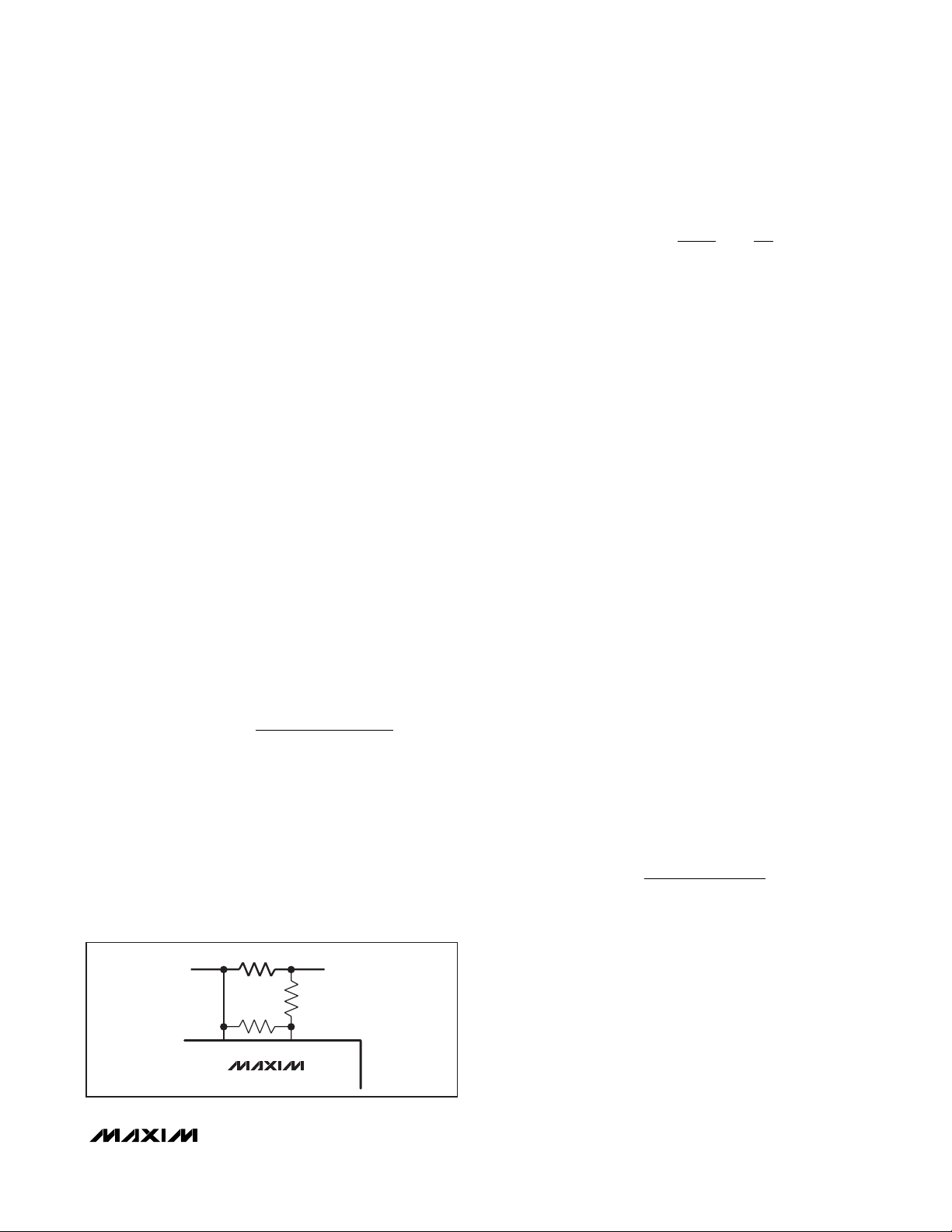
CSSN to tune the setting (Figure 4).
To minimize power dissipation, first choose RS1
according to the closest available value. For convenience, choose Ra = 6kΩ and calculate Rb from the
above equation.
Choose a current-sense resistor (RS1) to have a sufficient power rating to handle the full system current. The
current-sense resistor can be reduced to improve efficiency, but this degrades accuracy due to the currentsense amplifier’s input offset (0.15mV typ). See
Typical
Operating Characteristics
to estimate the input current-
limit accuracy at various set points.
Automatic Power-Source Selection
The MAX17005/MAX17006/MAX17015 use an external
charge pump to drive the gate of an n-channel adapter
selection switch (N3 and Q1a). In Figure 1, when the
adapter is present, BST is biased 5V above V
ADAPTER
so that N3 and Q1a are on, and Q1b is off. As long as
the adapter is present, even though the charger is off,
the power stage forces a refresh pulse to the BST
charge pump every 5ms.
When the adapter voltage is removed, the charger
stops generating BST refresh pulses and N4 forces N2
off, Q1b turns on and supplies power to the system
from the battery.
In Figure 1, D1 must have low forward-voltage drop and
low reverse-leakage current to ensure sufficient gate
drive at N3 and Q1a. A 100mA, low reverse-leakage
Schottky diode is the right choice.
Analog Input Current-Monitor Output
Use IINP to monitor the system-input current, which is
sensed across CSSP and CSSN. The voltage at IINP is
proportional to the input current:
where I
INPUT
is the DC current supplied by the AC
adapter, G
IINP
is the transconductance of the sense
amplifier (2.8 mA/V typ), and R
IINP
is the resistor connected between IINP and ground. Typically, IINP has a
0V to 3.5V output voltage range. Leave IINP unconnected when not used.
Figure 4. Input Current-Limit Fine Tuning
II
=+
INPUT LOAD
IV
CHARGE BATTERY
RS1
Ra
×
V
×η
IN
Rb
mV
I
INPUT LIMIT_
60
RS
1
Rb
()=×+
1
Ra
V
I
=
INPUT
RS G R
IINP
××1
IINP IINP
CSSP CSSN
MAX17005/MAX17006/MAX17015

MAX17005/MAX17006/MAX17015
1.2MHz Low-Cost,
High-Performance Chargers
14 ______________________________________________________________________________________
IINP can also be used to monitor battery discharge current (see Figure 5). In the MAX17015, when the adapter is
absent, drive ISET above 1V to enable IINP during battery
discharge. When the adapter is reinserted, ISET must be
released to the correct control level within 300ms.
AC Adapter Detection
The MAX17005/MAX17006/MAX17015 include a hysteretic comparator that detects the presence of an AC
power adapter. When ACIN is lower than 2.1V, the
open-drain ACOK output becomes high impedance.
Connect a 10kΩ pullup resistance between LDO and
ACOK. Use a resistive voltage-divider from the
adapter’s output to the ACIN pin to set the appropriate
detection threshold. Select the resistive voltage-divider
so that the voltage on ACIN does not to exceed its
absolute maximum rating (6V).
LDO Regulator and V
AA
An integrated low-dropout (LDO) linear regulator provides a 5.4V supply derived from DCIN, and delivers
over 40mA of load current. Do not use the LDO to
external loads greater than 10mA. The LDO powers the
gate drivers of the n-channel MOSFETs. See the
MOSFET Drivers
section. Bypass LDO to PGND with a
4.7μF ceramic capacitor. VAAis 4.2V reference supplied by DCIN. VAAbiases most of the control circuitry,
and should be bypassed to GND with a 1μF or greater
ceramic capacitor.
Operating Conditions
The MAX17005/MAX17006/MAX17015 have the following
operating states:
• Adapter Present: When DCIN is greater than 8.7V,
the controller detects the adapter. In this condition,
both the LDO and VAAturn on and battery charging
is allowed:
a) Charging: The total MAX17005/MAX17006/
MAX17015 quiescent current when charging is
3mA (max) plus the current required to drive the
MOSFETs.
b) Not Charging: To disable charging drive ISET
below 26mV. When the adapter is present and
charging is disabled, the total adapter quiescent
current is less than 1.5mA and the total battery
quiescent current is less than 60μA. The charge
pump still operates.
• Adapter Absent (Power Fail): When V
DCIN
is less
than V
CSIN
+ 120mV, the DC-DC converter is in
dropout. The charger detects the dropout condition
and shuts down.
The MAX17005/MAX17006/MAX17015 allow charging
under the following conditions:
• DCIN > 7.5V, LDO > 4V, VAA> 3.1V
•V
DCIN
> V
CSIN
+ 420mV (300mV falling hysteresis)
•V
ISET
> 45mV or PWM detected
____________________DC-DC Converter
The MAX17005/MAX17006/MAX17015 employ a synchronous step-down DC-DC converter with an n-channel high-side MOSFET switch and an n-channel
low-side synchronous rectifier. The charger features a
controlled inductor current-ripple architecture, currentmode control scheme with cycle-by-cycle current limit.
The controller’s off-time (t
OFF
) is adjusted to keep the
high-side MOSFET junction temperature constant. In
this way, the controller switches faster when the highside MOSFET has available thermal capacity. This
allows the inductor current ripple and the output-voltage ripple to decrease so that smaller and cheaper
components can be used. The controller can also operate in discontinuous conduction mode for improved
light-load efficiency.
Figure 5. Current-Monitoring Design Battery Discharge
Q1a
RS1
15mΩ
C7
10nF
CSSP CSSN
MAX17015
BST
DHI
SYSTEM LOAD
C
IN
ADAPTER
R6
50kΩ
D1
C4
0.1μF
N1
LX
Q1b
BATTERY

MAX17005/MAX17006/MAX17015
1.2MHz Low-Cost,
High-Performance Chargers
______________________________________________________________________________________ 15
The operation of the DC-to-DC controller is determined
by the following five comparators as shown in the functional diagram in Figures 2 and 6:
• The IMIN comparator triggers a pulse in discontinuous mode when the accumulated error is too high.
IMIN compares the control signal (LVC) against
10mV (referred at V
CSIP
- V
CSIN
). When LVC is less
than this threshold, DHI and DLO are both forced
low. Indirectly, IMIN sets the peak inductor current
in discontinuous mode.
• The CCMP comparator is used for current-mode
regulation in continuous-conduction mode. CCMP
compares LVC against the inductor current. The
high-side MOSFET on-time is terminated when the
CSI voltage is higher than LVC.
• The IMAX comparator provides a secondary cycleby-cycle current limit. IMAX compares CSI to
110mV (corresponding to 11A when RS2 = 10mΩ).
The high-side MOSFET on-time is terminated when
the current-sense signal exceeds 11A. A new cycle
cannot start until the IMAX comparator’s output
goes low.
• The ZCMP comparator provides zero-crossing detection during discontinuous conduction. ZCMP compares the current-sense feedback signal to 1A (RS2
= 10mΩ). When the inductor current is lower than
the 1A threshold, the comparator output is high,
and DLO is turned off.
• The OVP comparator is used to prevent overvoltage
at the output due to battery removal. OVP compares BATT against the VCTL. When BATT is
100mV/cell above the set value, the OVP comparator output goes high, and the high-side MOSFET
on-time is terminated. DHI and DLO remain off until
the OVP condition is removed.
SET POINT + 100mV
Figure 6. DC-DC Converter Functional Diagram
CSI
BDIV
OVP
IMAX
11A
CCMP
LVC
IMIN
1A
ZCMP
1A
CSSP
CSIN
OFF-TIME
COMPUTE
R
S
Q
Q
OFF-TIME
ONE SHOT
DH DRIVER
DL DRIVER
MAX17005/MAX17006/MAX17015
1.2MHz Low-Cost,
High-Performance Chargers
16 ______________________________________________________________________________________
CC, CCI, CCS, and LVC Control Blocks
The MAX17005/MAX17006/MAX17015 control input
current (CCS control loop), charge current (CCI control
loop), or charge voltage (CC control loop), depending
on the operating condition. The three control loops, CC,
CCI, and CCS are brought together internally at the
lowest voltage clamp (LVC) amplifier. The output of the
LVC amplifier is the feedback control signal for the
DC-DC controller. The minimum voltage at the CC, CCI,
or CCS appears at the output of the LVC amplifier and
clamps the other control loops to within 0.3V above the
control point. Clamping the other two control loops
close to the lowest control loop ensures fast transition
with minimal overshoot when switching between different control loops (see the
Compensation
section). The
CCS and CCI loops are compensated internally, and
the CC loop is compensated externally.
Continuous-Conduction Mode
With sufficiently large charge current, the MAX17005/
MAX17006/MAX17015s’ inductor current never crosses
zero, which is defined as continuous-conduction mode.
The controller starts a new cycle by turning on the highside MOSFET and turning off the low-side MOSFET.
When the charge-current feedback signal (CSI) is
greater than the control point (LVC), the CCMP comparator output goes high and the controller initiates the
off-time by turning off the high-side MOSFET and turning on the low-side MOSFET. The operating frequency
is governed by the off-time and is dependent upon
V
CSIN
and V
DCIN
.
The on-time can be determined using the following
equation:
where:
The switching frequency can then be calculated:
At the end of the computed off-time, the controller initiates a new cycle if the control point (LVC) is greater
than 10mV (V
CSIP
- V
CSIN
referred), and the charge
current is less than the cycle-by-cycle current limit.
Restated another way, IMIN must be high, IMAX must
be low, and OVP must be low for the controller to initiate a new cycle. If the peak inductor current exceeds
IMAX comparator threshold or the output voltage
exceeds the OVP threshold, then the on-time is terminated. The cycle-by-cycle current limit effectively protects against overcurrent and short-circuit faults.
If during the off-time the inductor current goes to zero,
the ZCMP comparator output pulls high, turning off the
low-side MOSFET. Both the high- and low-side
MOSFETs are turned off until another cycle is ready to
begin. ZCOMP causes the MAX17005/MAX17006/
MAX17015 to enter into the discontinuous conduction
mode (see the
Discontinuous Conduction
section).
Discontinuous Conduction
The MAX17005/MAX17006/MAX17015 can also operate
in discontinuous conduction mode to ensure that the
inductor current is always positive. The MAX17005/
MAX17006/MAX17015 enter discontinuous conduction
mode when the output of the LVC control point falls below
10mV (referred at V
CSIP
- V
CSIN
). For RS2 = 10mΩ, this
corresponds to a peak inductor current of 1A.
In discontinuous mode, a new cycle is not started until
the LVC voltage rises above IMIN. Discontinuous mode
operation can occur during conditioning charge of
overdischarged battery packs, when the charge current has been reduced sufficiently by the CCS control
loop, or when the charger is in constant-voltage mode
with a nearly full battery pack.
Compensation
The charge voltage, charge current, and input currentlimit regulation loops are compensated separately. The
charge current and input current-limit loops, CCI and
CCS, are compensated internally, whereas the charge
voltage loop is compensated externally at CC.
t
ON
I
RI PPLE
f
LI
×
=
SW
RI PPLE
VV
DCIN BATT
Vt
BATT OFF
=
=
tt
+
ON OFF
−
×
L
1

MAX17005/MAX17006/MAX17015
1.2MHz Low-Cost,
High-Performance Chargers
______________________________________________________________________________________ 17
CC Loop Compensation
The simplified schematic in Figure 7 is sufficient to
describe the operation of the controller’s voltage loop,
CC. The required compensation network is a pole-zero
pair formed with CCCand RCC. The zero is necessary
to compensate the pole formed by the output capacitor
and the load. R
ESR
is the equivalent series resistance
(ESR) of the charger output capacitor (C
OUT
). RLis the
equivalent charger output load, where RL= ΔV
BATT
/
ΔI
CHG
. The equivalent output impedance of the GMV
amplifier, R
OGMV
, is greater than 10MΩ. The voltage-
amplifier transconductance, GMV = 0.125μA/mV. The
DC-DC converter transconductance is dependent upon
charge current-sense resistor RS2:
where A
CSI
= 20, and RS2 = 10mΩ in the typical appli-
cation circuits, so GM
OUT
= 5A/V.
The loop transfer function is given by:
The poles and zeros of the voltage-loop transfer function
are listed from lowest frequency to highest frequency in
Table 2.
Near crossover, CCCis much lower impedance than
R
OGMV
. Since CCCis in parallel with R
OGMV, CCC
dominates the parallel impedance near crossover. Additionally,
RCCis much higher impedance than CCCand dominates
the series combination of RCCand CCC, so:
C
OUT
is also much lower impedance than RLnear
crossover so the parallel impedance is mostly capacitive and:
Table 2. CC Loop Poles and Zeros
f
RC
PCV
OGMV CC
_
=
×
1
2π
f
RC
ZCV
CC CC
_
=
×
1
2π
f
RC
POUT
LOUT
_
=
×
1
2π
f
RC
ZOUT
ESR OUT
_
=
×
1
2π
Figure 7. CC Loop Diagram
BATT
GM
OUT
R
ESR
R
C
OUT
CC
GMV
R
CC
C
CC
R
OGMV
VCTL
L
GM =
OUT
CSI ×
1
2ARS
LTF R GMV R
=×××
GM
OUT L OGMV
sC R
+×
(1 ))( )
×
OUT ESR
()()
11
+× + ×
sC R sC R
CC O GMV OUT L
1
+×
sC R
CC CC
RsCR
×+ ×
()
OGMV CC CC
1
sC R
+×
()
1
CC OGMV
R
≅
CC
R
L
sC R sC
()11+×
OUT L OUT
≅
NAME EQUATION DESCRIPTION
CCV Pole Lowest frequency pole created by CCVand GMV’s finite output resistance.
Voltage-loop compensation zero. If this zero is at the same frequency or lower
CCV Zero
Output
Pole
Output
Zero
than output pole f
response near the crosso ver frequency. Choose C
lea st one decade below crosso ver to ensure adequate phase margin.
Output pole formed with the effective load resi stance R
capacitance C
of the system or the crossover frequency.
Output ESR Zero. This zero can keep the loop from crossing unit y gain if
is less than the desired crossover frequency; therefore, choose a
f
Z_OUT
capacitor with an ESR zero greater than the crossover frequency.
OUT
, the loop-transfer function approximate s a single-pole
P_OUT
. RLinfluences the DC gain but does not affect the stability
to place thi s zero at
CV
and the output
L

MAX17005/MAX17006/MAX17015
1.2MHz Low-Cost,
High-Performance Chargers
18 ______________________________________________________________________________________
If R
ESR
is small enough, its associated output zero has
a negligible effect near crossover and the loop-transferfunction can be simplified as follows:
Setting LTF = 1 to solve for the unity-gain frequency
yields:
For stability, choose a crossover frequency lower than
1/10 the switching frequency (f
OSC)
. For example,
choose a crossover frequency of 50kHz and solve for
RCCusing the component values listed in Figure 1 to
yield R
CC
= 3kΩ:
GMV = 0.125μA/mV
GM
OUT
= 5A/V
C
OUT
= 4.7μF
f
OSC_CV
= 600kHz
RL = 0.2Ω
f
CO_CV
= 50kHz
To ensure that the compensation zero adequately cancels the output pole, select f
Z_CV
≤ f
P_OUT
:
CCC≥ (RL/RCC) x C
OUT
CCC≥ 300pF (assuming 2 cells and 2A maximum
charge current).
Figure 8 shows the Bode plot of the voltage-loopfrequency response using the values calculated above.
MOSFET Drivers
The DHI and DLO outputs are optimized for driving
moderate-sized power MOSFETs. The MOSFET drive
capability is the same for both the low-side and highsides switches. This is consistent with the variable duty
factor that occurs in the notebook computer environment where the battery voltage changes over a wide
range. There must be a low-resistance, low-inductance
path from the DLO driver to the MOSFET gate to prevent shoot-through. Otherwise, the sense circuitry in the
MAX17005/MAX17006 interpret the MOSFET gate as
“off” while there is still charge left on the gate. Use very
short, wide traces measuring 10 to 20 squares or fewer
(1.25mm to 2.5mm wide if the MOSFET is 25mm from
the device). Unlike the DLO output, the DHI output uses
a 50ns (typ) delay time to prevent the low-side MOSFET
from turning on until DHI is fully off. The same considerations should be used for routing the DHI signal to the
high-side MOSFET.
The high-side driver (DHI) swings from LX to 5V above
LX (BST) and has a typical impedance of 1.5Ω sourcing
and 0.8Ω sinking. The strong high-side MOSFET driver
eliminates most of the power dissipation due to switching losses. The low-side driver (DLO) swings from LDO
to ground and has a typical impedance of 3Ω sinking
and 3Ω sourcing. This helps prevent DLO from being
pulled up when the high-side switch turns on due to
capacitive coupling from the drain to the gate of the
low-side MOSFET. This places some restrictions on the
MOSFETs that can be used. Using a low-side
MOSFET with smaller gate-to-drain capacitance can
prevent these problems.
Design Procedure
MOSFET Selection
Choose the n-channel MOSFETs according to the maximum required charge current. The MOSFETs must be
able to dissipate the resistive losses plus the switching
losses at both V
DCIN(MIN)
and V
DCIN(MAX)
.
For the high-side MOSFET, the worst-case resistive
power losses occur at the maximum battery voltage
and minimum supply voltage:
Figure 8. CC Loop Response
R
LTF GM
=×
OUT
sC
CC
OUT
G
MV
fGMG
CO CV OUT MV
=××
_
R
CC
×2π
C
OUT
R
CC
π
=
×
GMV GM
Cf
×2
OUT CO CV
×
_
OUT
k
≅
Ω
3
80
60
0
40
-45
20
MAGNITUDE (dB)
0
-20
-40
0.1 1M
MAG
PHASE
FREQUENCY (Hz)
PHASE (DEGREES)
-90
-135
100k10k1k100101
PD HighSide
()
COND
V
BATT MAX
V
DCIN MIN
()
()
=×
I
CHG
2
××R
DS ON()

MAX17005/MAX17006/MAX17015
1.2MHz Low-Cost,
High-Performance Chargers
______________________________________________________________________________________ 19
Generally, a low gate charge high-side MOSFET is preferred to minimize switching losses. However, the
R
DS(ON)
required to stay within package power dissipation often limits how small the MOSFET can be. The
optimum occurs when the switching losses equal the
conduction losses. High-side switching losses do not
usually become an issue until the input is greater than
approximately 15V. Calculating the power dissipation in
N1 due to switching losses is difficult since it must
allow for difficult quantifying factors that influence the
turn-on and turn-off times. These factors include the
internal gate resistance, gate charge, threshold voltage, source inductance, and PCB layout characteristics. The following switching-loss calculation provides
only a very rough estimate and is no substitute for
breadboard evaluation, preferably including a verification using a thermocouple mounted on N1:
where t
TRANS
is the drivers transition time and can be
calculated as follows:
I
GSRC
and I
GSNK
are the peak gate-drive source/sink
current (3Ω sourcing and 0.8Ω sinking, typically). The
MAX17005/MAX17006/MAX17015 control the switching
frequency as shown in the
Typical Operating
Characteristics
.
The following is the power dissipated due to high-side
n-channel MOSFET’s output capacitance (C
RSS
):
The following high-side MOSFET’s loss is due to the
reverse-recovery charge of the low-side MOSFET’s
body diode:
Ignore PD
QRR
(HighSide) if a Schottky diode is used
parallel to a low-side MOSFET.
The total high-side MOSFET power dissipation is:
Switching losses in the high-side MOSFET can become
an insidious heat problem when maximum AC adapter
voltages are applied. If the high-side MOSFET chosen
for adequate R
DS(ON)
at low-battery voltages becomes
hot when biased from V
DCIN(MAX)
, consider choosing
another MOSFET with lower parasitic capacitance.
For the low-side MOSFET (N2), the worst-case power
dissipation always occurs at maximum input voltage:
The following additional loss occurs in the low-side
MOSFET due to the body diode conduction losses:
The total power low-side MOSFET dissipation is:
These calculations provide an estimate and are not a
substitute for breadboard evaluation, preferably
including a verification using a thermocouple mounted
on the MOSFET.
Inductor Selection
The selection of the inductor has multiple trade-offs
between efficiency, transient response, size, and cost.
Small inductance is cheap and small, and has a better
transient response due to higher slew rate; however, the
efficiency is lower because of higher RMS current. High
inductance results in lower ripple so that the need of the
output capacitors for output voltage ripple goes low.
The MAX17005/MAX17006/MAX17015 combine all the
inductor trade-offs in an optimum way by controlling
switching frequency. High-frequency operation permits
the use of a smaller and cheaper inductor, and consequently results in smaller output ripple and better transient response.
The charge current, ripple, and operating frequency
(off-time) determine the inductor characteristics. For
optimum efficiency, choose the inductance according
to the following equation:
where k = 35ns/V.
1
()=× × × ×
2
PD HS t V I f
SW TRA NS CSSP CHG SW
t
TRANS
⎛
11
=+
⎜
II
⎝
GSRC GSNK
⎞
QQ
×+
()
GD GS
⎟
⎠
2
PD HS
CRSS
()≈
VCf
××
CSSP RSS SW
2
QV f
××
2
RR CSSP SW
2
PD HS
()=
QRR
PD HS PD HS PD HS
() () ()≈+
TOTAL COND SW
() ()++PD HS PD HS
CRSS QRR
PD LS
COND
()
⎛
V
=−
⎜
V
⎝
BATT MIN
CSSP MAX
⎞
()
×1
⎟
⎠
()
I
CH
R2×
GGDSON
()
PD LS I V
() . .=× ×005 04
BDY PEAK
PD LS PD LS PD LS
() () ()≈+
TOTAL COND BDY
L
=
4
ILIR
××
CHG MAX
kV
×
IN
2

MAX17005/MAX17006/MAX17015
1.2MHz Low-Cost,
High-Performance Chargers
20 ______________________________________________________________________________________
For optimum size and inductor current ripple, choose
LIR
MAX
= 0.4, which sets the ripple current to 40% the
charge current and results in a good balance between
inductor size and efficiency. Higher inductor values
decrease the ripple current. Smaller inductor values
save cost but require higher saturation current capabilities and degrade efficiency.
Inductor L1 must have a saturation current rating of at
least the maximum charge current plus 1/2 the ripple
current (ΔIL):
I
SAT
= I
CHG
+ (1/2) ΔIL
The ripple current is determined by:
Input Capacitor Selection
The input capacitor must meet the ripple current
requirement (I
RMS
) imposed by the switching currents.
Nontantalum chemistries (ceramic, aluminum, or
OS-CON) are preferred due to their resilience to powerup and surge currents:
The input capacitors should be sized so that the temperature rise due to ripple current in continuous conduction does not exceed approximately 10°C. The
maximum ripple current occurs at 50% duty factor or
V
DCIN
= 2 x V
BATT
, which equates to 0.5 x I
CHG
. If the
application of interest does not achieve the maximum
value, size the input capacitors according to the worstcase conditions.
Output Capacitor Selection
The output capacitor absorbs the inductor ripple current and must tolerate the surge current delivered from
the battery when it is initially plugged into the charger.
As such, both capacitance and ESR are important
parameters in specifying the output capacitor as a filter
and to ensure the stability of the DC-to-DC converter
(see the
Compensation
section.) Beyond the stability
requirements, it is often sufficient to make sure that the
output capacitor’s ESR is much lower than the battery’s
ESR. Either tantalum or ceramic capacitors can be
used on the output. Ceramic devices are preferable
because of their good voltage ratings and resilience to
surge currents. Choose the output capacitor based on:
Choose k
CAP-BIAS
is a derating factor of 2 for typical 25V-
rated ceramic capacitors.
For fSW= 800kHz, I
RIPPLE
= 1A, and to get ΔV
BATT
=
70mV, choose C
OUT
as 4.7μF.
If the internal resistance of battery is close to the ESR of
the output capacitor, the voltage ripple is shared with
the battery and is less than calculated.
Applications Information
Setting Input Current Limit
The input current limit should be set based on the current capability of the AC adapter and the tolerance of
the input current limit. The upper limit of the input current threshold should never exceed the adapter’s minimum available output current. For example, if the
adapter’s output current rating is 5A ±10%, the input
current limit should be selected so that its upper limit is
less than 5A × 0.9 = 4.5A. Since the input current-limit
accuracy of the MAX17005/MAX17006/MAX17015 is
±3%, the typical value of the input current limit should
be set at 4.5A/1.03 ≈ 4.36A. The lower limit for input
current must also be considered. For chargers at the
low end of the spec, the input current limit for this
example could be 4.36A × 0.95 or approximately 4.14A.
Layout and Bypassing
Bypass DCIN with a 0.1μF ceramic to ground (Figure 1).
N1 and N2 protect the MAX17005/MAX17006/
MAX17015 when the DC power source input is reversed.
Bypass VAA, CSSP, and LDO as shown in Figure 1.
Good PCB layout is required to achieve specified noise
immunity, efficiency, and stable performance. The PCB
layout designer must be given explicit instructions—
preferably, a sketch showing the placement of the
power switching components and high current routing.
Refer to the PCB layout in the MAX17005/MAX17006/
MAX17015 evaluation kit for examples. A ground plane
is essential for optimum performance. In most applications, the circuit is located on a multilayer board, and
full use of the four or more copper layers is recommended. Use the top layer for high-current connections, the bottom layer for quiet connections, and the
inner layers for an uninterrupted ground plane.
Use the following step-by-step guide:
1) Place the high-power connections first, with their
grounds adjacent:
a) Minimize the current-sense resistor trace lengths,
and ensure accurate current sensing with Kelvin
connections.
b) Minimize ground trace lengths in the high-current
paths.
Δ=
2
×ILkV
IN
L
4
II
RMS CHG
⎛
VVV
×−
BATT DCIN BATT
=
⎜
×
⎜
⎝
()
V
DCIN
⎞
⎟
⎟
⎠
C
=
OUT
fV
××
SW BATT
I
RI PPLE
8 Δ
k
×
CAP BIAS
−

MAX17005/MAX17006/MAX17015
1.2MHz Low-Cost,
High-Performance Chargers
______________________________________________________________________________________ 21
c) Minimize other trace lengths in the high-current
paths.
d) Use > 5mm wide traces in the high-current
paths.
e) Connect CINto high-side MOSFET (10mm max
length).
f) Minimize the LX node (MOSFETs, rectifier cath-
ode, inductor (15mm max length)). Keep LX on
one side of the PCB to reduce EMI radiation.
Ideally, surface-mount power components are flush
against one another with their ground terminals
almost touching. These high-current grounds are
then connected to each other with a wide, filled
zone of top-layer copper, so they do not go through
vias. The resulting top-layer subground plane is
connected to the normal inner-layer ground plane
at the paddle. Other high-current paths should also
be minimized, but focusing primarily on short
ground and current-sense connections eliminates
about 90% of all PCB layout problems.
2) Place the IC and signal components. Keep the
main switching node (LX node) away from sensitive
analog components (current-sense traces and V
AA
capacitor). Important: the IC must be no further than
10mm from the current-sense resistors. Quiet connections to V
AA
and CC should be returned to a separate ground (GND) island. There is very little current
flowing in these traces, so the ground island need not
be very large. When placed on an inner layer, a sizable ground island can help simplify the layout
because the low-current connections can be made
through vias. The ground pad on the backside of the
package should also be connected to this quiet
ground island.
3) Keep the gate drive traces (DHI and DLO) as short
as possible (L < 20mm), and route them away from
the current-sense lines and VAA. These traces
should also be relatively wide (W > 1.25mm).
4) Place ceramic bypass capacitors close to the IC.
The bulk capacitors can be placed further away.
Place the current-sense input filter capacitors under
the part, connected directly to the GND pin.
5) Use a single-point star ground placed directly
below the part at the PGND pin. Connect the power
ground (ground plane) and the quiet ground island
at this location.

MAX17005/MAX17006/MAX17015
1.2MHz Low-Cost,
High-Performance Chargers
22 ______________________________________________________________________________________
Pin Configuration
Chip Information
TRANSISTOR COUNT: 12,990
PROCESS: BiCMOS
Minimal Operating Circuit
ADAPTER
SYSTEM
ADAPTER
DCIN
BATT
LDO
V
AA
GND
IINP
VCTL
ISET
CSSP CSSN
MAX17005
MAX17006
MAX17015
ACOK
BST
DHI
LX
DLO
PGND
CSIP
CSIN
BATT
CC
ACIN
TOP VIEW
BST
DHI
15 14 12 11
DLO
LDO
13
PGND
BATTERY
ISET
IINP
10
CSSN
9
8
CSSP
ACOK
7
BATT
6
ACIN
V
VCTL
CC
LX
16
17
EXPOSED PADDLE
1 2
DCIN
MAX17005
MAX17006
MAX17015
3
CSIP
AGND
45
CSIN
18
AA
19
20
THIN QFN
4mm x 4mm

MAX17005/MAX17006/MAX17015
1.2MHz Low-Cost,
High-Performance Chargers
______________________________________________________________________________________ 23
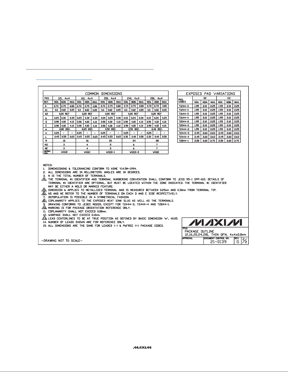
Package Information
(The package drawing(s) in this data sheet may not reflect the most current specifications. For the latest package outline information
go to www.maxim-ic.com/packages
.)
24L QFN THIN.EPS
MAX17005/MAX17006/MAX17015
1.2MHz Low-Cost,
High-Performance Chargers
Maxim cannot assume responsibility for use of any circuitry other than circuitry entirely embodied in a Maxim product. No circuit patent licenses are
implied. Maxim reserves the right to change the circuitry and specifications without notice at any time.
24
____________________Maxim Integrated Products, 120 San Gabriel Drive, Sunnyvale, CA 94086 408-737-7600
© 2008 Maxim Integrated Products is a registered trademark of Maxim Integrated Products, Inc.
Package Information (continued)
(The package drawing(s) in this data sheet may not reflect the most current specifications. For the latest package outline information
go to www.maxim-ic.com/packages
.)
 Loading...