General Description
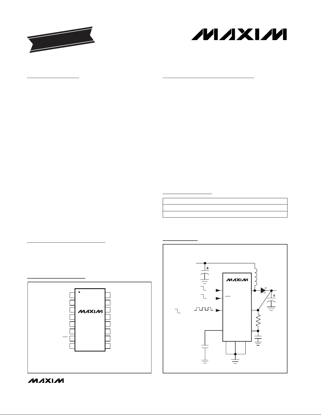
The MAX1700/MAX1701 are high-efficiency, low-noise,
step-up DC-DC converters intended for use in batterypowered wireless applications. They use a synchronous-rectified pulse-width-modulation (PWM) boost
topology to generate 2.5V to 5.5V outputs from battery
inputs such as one to three NiCd/NiMH cells or one LiIon cell. Both devices have an internal 1A, 130mΩ N-
channel MOSFET switch and a 250mΩ P-channel
synchronous rectifier.
With their internal synchronous rectifier, the MAX1700/
MAX1701 deliver 5% better efficiency than similar nonsynchronous converters. They also feature a pulsefrequency-modulation (PFM) standby mode to improve
efficiency at light loads, and a 3µA shutdown mode.
The MAX1700/MAX1701 come in 16-pin QSOP packages (which occupy the same space as an 8-pin SO).
The MAX1701 includes two comparators to generate
power-good and low-battery warning outputs. It also
contains a gain block that can be used to build a linear
regulator using an external P-channel pass device.
For higher-power outputs, refer to the MAX1703. For
dual outputs (step-up and linear regulator), refer to the
MAX1705/MAX1706. For an on-board analog-to-digital
converter, refer to the MAX848/MAX849.
The MAX1701 evaluation kit is available to speed design
time.
Applications
Digital Cordless Phones Personal Communicators
PCS Phones Palmtop Computers
Wireless Handsets Hand-Held Instruments
Two-Way Pagers
Features
♦ Up to 96% Efficiency
♦ 1.1 VINGuaranteed Start-Up
♦ 0.7V to 5.5V Input Range
♦ Up to 800mA Output
♦ Step-Up Output (adjustable from 2.5V to 5.5V)
♦ PWM/PFM Synchronous-Rectified Topology
♦ External Clock or Internal 300kHz Oscillator
♦ 3µA Logic-Controlled Shutdown
♦ Power-Good Output (MAX1701)
♦ Low-Battery Comparator (MAX1701)
♦ Uncommitted Gain Block (MAX1701)
MAX1700/MAX1701
1-Cell to 3-Cell, High-Power (1A),
Low-Noise, Step-Up DC-DC Converters
________________________________________________________________
Maxim Integrated Products
1
PGNDGNDFB
ONA
REF
ONB
POUT
LX
OUT
ON
INPUT
0.7V TO 5.5V
OR
OFF
OFF
ON
SYNC
PWM
PFM
OUTPUT
3.3V OR ADJ
UP TO 800mA
CLK/SEL
MAX1700
Pin Configurations
TOP VIEW
16
15
14
13
12
11
10
9
1
2
3
4
5
6
7
8
I.C. I.C.
POUT
OUT
LX
PGND
FB
I.C.
I.C.
I.C. = INTERNAL CONNECTION. LEAVE OPEN OR CONNECT TO GND
MAX1700
QSOP
I.C.
REF
I.C.
CLK/SEL
GND
ONB
ONA
Typical Operating Circuit
19-4759; Rev 1; 1/99
PART
MAX1700EEE
-40°C to +85°C
TEMP. RANGE PIN-PACKAGE
16 QSOP
EVALUATION KIT MANUAL
FOLLOWS DATA SHEET
Ordering Information
MAX1701EEE
-40°C to +85°C 16 QSOP
Pin Configurations continued at end of data sheet.
For free samples & the latest literature: http://www.maxim-ic.com, or phone 1-800-998-8800.
For small orders, phone 1-800-835-8769.
MAX1700/MAX1701
1-Cell to 3-Cell, High-Power (1A),
Low-Noise, Step-Up DC-DC Converters
2 _______________________________________________________________________________________
ABSOLUTE MAXIMUM RATINGS
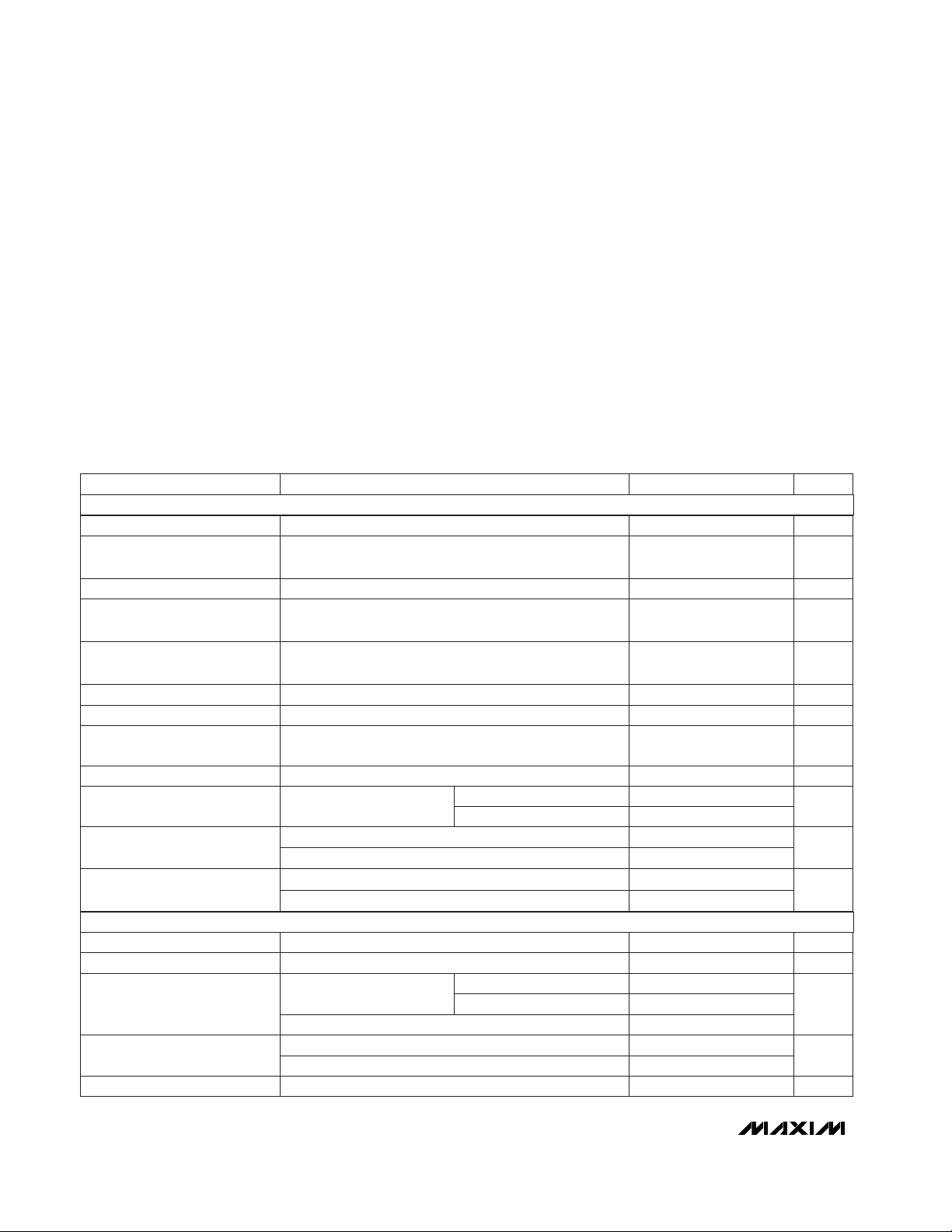
ELECTRICAL CHARACTERISTICS
(CLK/SEL = ONA = ONB = FB = PGND = GND, OUT = POUT, V
OUT
= 3.6V (Note 6); MAX1701: AIN = LBN = GND, LBP = REF,
T
A
= 0°C to +85°C, unless otherwise noted. Typical values are at TA = +25°C.)
Stresses beyond those listed under “Absolute Maximum Ratings” may cause permanent damage to the device. These are stress ratings only, and functional
operation of the device at these or any other conditions beyond those indicated in the operational sections of the specifications is not implied. Exposure to
absolute maximum rating conditions for extended periods may affect device reliability.
ONA, ONB, OUT, AO, POK, LBO to GND...................-0.3V, +6V
PGND to GND.....................................................................±0.3V
LX to PGND.....................................................-0.3V,V
POUT
+0.3V
CLK/SEL, AIN, REF, FB, LBP, LBN, POUT to GND............-0.3V,
V
OUT
+0.3V ...................................................................................
Continuous Power Dissipation (T
A
=+70°C)
16-QSOP (Derate 8.30mW/°C above +70°C) ...............667mW
Operating Temperature Ranges
MAX1700EEE, MAX1701EEE ...........................-40°C to +85°C
Junction Temperature......................................................+150°C
Storage Temperature Range.............................-65°C to +160°C
Lead Temperature (soldering, 10sec).............................+300°C
CLK/SEL = GND
CLK/SEL = GND
CLK/SEL = OUT
I
LOAD
< 1mA, TA= +25°C
P-channel
N-channel
VLX= V
ONB
= V
OUT
= 5.5V
VLX= 0V, V
OUT
= 5.5V
V
ONB
= 3.6V
CLK/SEL = OUT, No load to full load
CLK/SEL = OUT (MAX1701)
CLK/SEL = OUT (MAX1700)
(Note 4)
V
OUT
= 1.5V
VFB< 0.1V, CLK/SEL = OUT, V
BATT
= 2.4V,
includes load regulation error for 0A ≤ I
LX
≤ 0.55A
Adjustable output, CLK/SEL = OUT, V
BATT
= 2.4V,
includes load regulation error for 0A ≤ I
LX
≤ 0.55A
CLK/SEL = GND (MAX1701)
VFB= 1.25V
CLK/SEL = GND (MAX1700)
CONDITIONS
mA20 120P-Channel Turn-Off Current
mA
250 400 550
N-Channel Current Limit
1100 1300 1600
Ω
0.25 0.5
Switch On-Resistance 0.13 0.28
0.2 0.45
µA0.1 20LX Leakage Current
µA0.1 20POUT Leakage Current
µA
140 300
125 250
Supply Current in Low-Noise
Mode (Note 6)
µA
55 110
Supply Current in Low-Power
Mode (Note 6)
35 70
V0.9 1.1
Minimum Start-Up Voltage
(Note 2)
V0.7 5.5Input Voltage Range (Note 1)
µA
320
Supply Current in Shutdown
%-1.6Load Regulation (Note 5)
V2.0 2.15 2.3
Output Voltage Lockout
Threshold
V2.5 5.5Output Voltage Adjust Range
kHz40 150 300Frequency in Start-Up Mode
V3.17 3.30 3.38Output Voltage (Note 3)
V1.210 1.24 1.255FB Regulation Voltage
nA0.01 20FB Input Current
UNITSMIN TYP MAXPARAMETER
CLK/SEL = GND
CLK/SEL = OUT
DC-DC CONVERTER
DC-DC SWITCHES
MAX1701
MAX1700 0.1 20
Input High Voltage (Note 7)
MAX1700/MAX1701
1-Cell to 3-Cell, High-Power (1A),
Low-Noise, Step-Up DC-DC Converters
_______________________________________________________________________________________ 3
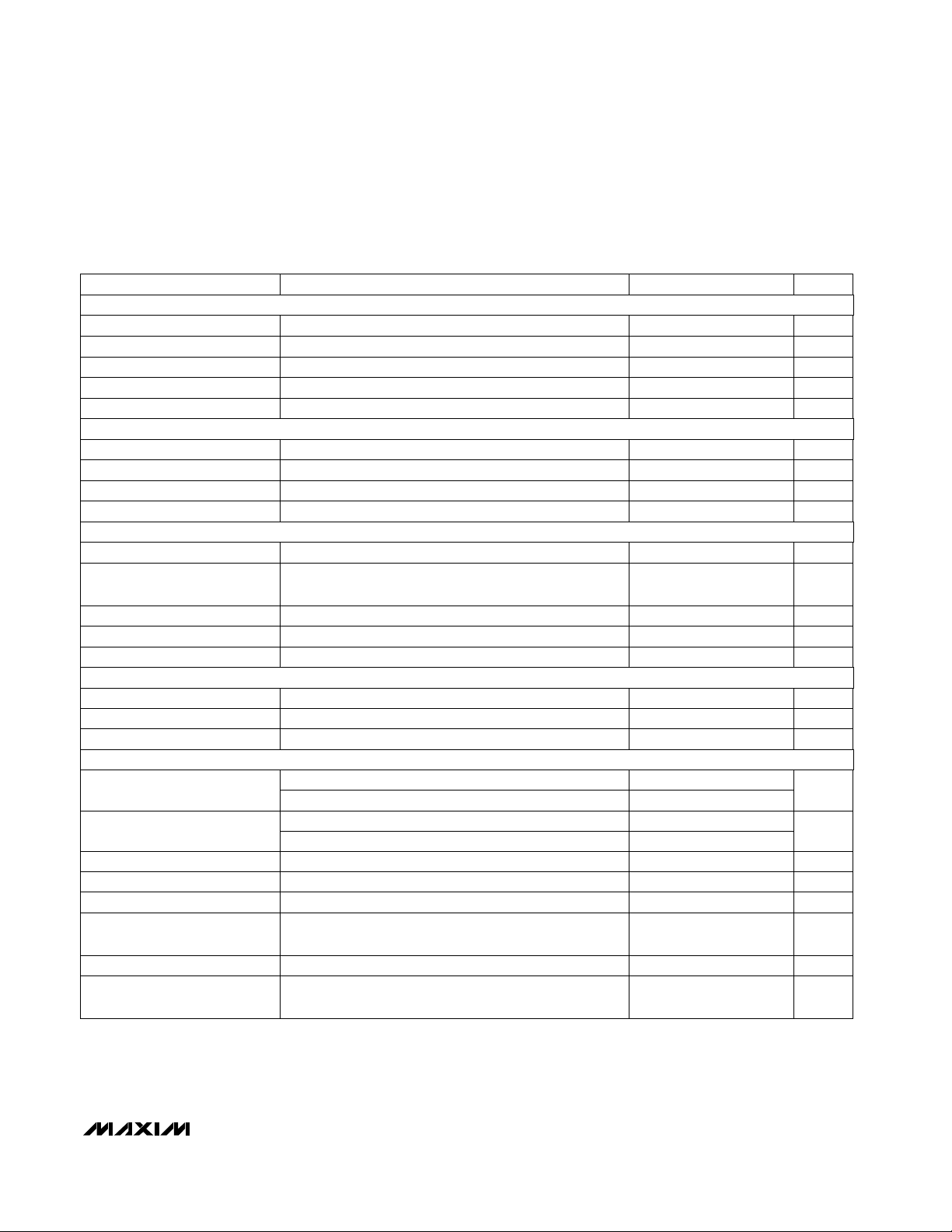
ELECTRICAL CHARACTERISTICS (continued)
(CLK/SEL = ONA = ONB = FB = PGND = GND, OUT = POUT, V
OUT
= 3.6V (Note 6); MAX1701: AIN = LBN = GND, LBP = REF,
T
A
= 0°C to +85°C, unless otherwise noted. Typical values are at TA = +25°C.)
-1µA < I
REF
< 50µA
I
REF
= 0
V
AIN
= 1.5V
I
SINK
= 1mA, V
OUT
= 3.6V or I
SINK
= 20µA, V
OUT
= 1V
To maintain input offset < ±5mV (at least one input must
be within this range)
IAO= 20µA
LBP falling, 15mV hysteresis
V
OUT
= V
POK
= 5.5V
I
SINK
= 1mA, V
OUT
= 3.6V or I
SINK
= 20µA, V
OUT
= 1V
Rising V
FB
Rising V
OUT
, VFB< 0.1V
10µA < IAO= 100µA
V
AIN
= 0.7V, IAO= 100µA
V
AIN
= 1.5V, VAO= 5.5V
CONDITIONS
mV515REF Load Regulation
V1.237 1.250 1.263Reference Output Voltage
V0.03 0.4LBO Output Low Voltage
V0.5 1.5
LBN, LBP Common Mode
Range
mV-5 ±0.5 5LBN, LBP Input Offset
µA0.01 1POK High Leakage Current
nA-30 30AIN Input Current
V1.237 1.25 1.263AIN Reference Voltage
V0.03 0.4POK Low Voltage
V1.1 1.12 1.14External Trip Level
V2.93 2.97 3.02Internal Trip Level
mmho5916Transconductance
V0.1 0.4AO Output Low Voltage
µA0.01 1AO Output High Leakage
UNITSMIN TYP MAXPARAMETER
V
LBP
= V
LBN
= 1.5V
V
OUT
= V
LBO
= 5V
nA20LBN, LBP Input Current
µA0.01 1LBO High Leakage
2.5V < V
OUT
< 5V mV0.2 5REF Supply Rejection
1.2V < V
OUT
< 5.5V, ONA and ONB
0.2V
OUT
1.2V < V
OUT
< 5.5V, ONA and ONB
2.5V < V
OUT
< 5.5V, CLK/SEL
0.8V
OUT
V
0.2V
OUT
Input Low Voltage (Note 7)
2.5V < V
OUT
< 5.5V, CLK/SEL
V
0.8V
OUT
Input High Voltage (Note 7)
CLK/SEL = OUT
ONA, ONB, and CLK/SEL
kHz260 300 340Internal Oscillator Frequency
µA-1 1Logic Input Current
kHz200 400
External Clock Frequency
Range
%80 86 90Oscillator Maximum Duty Cycle
ns100
Maximum CLK/SEL Rise/Fall
Time
ns200Minimum CLK/SEL Pulse Width
GAIN BLOCK (MAX1701)
POWER GOOD (MAX1701)
LOW-BATTERY COMPARATOR
REFERENCE
LOGIC AND CONTROL INPUTS
MAX1700/MAX1701
1-Cell to 3-Cell, High-Power (1A),
Low-Noise, Step-Up DC-DC Converters
4 _______________________________________________________________________________________
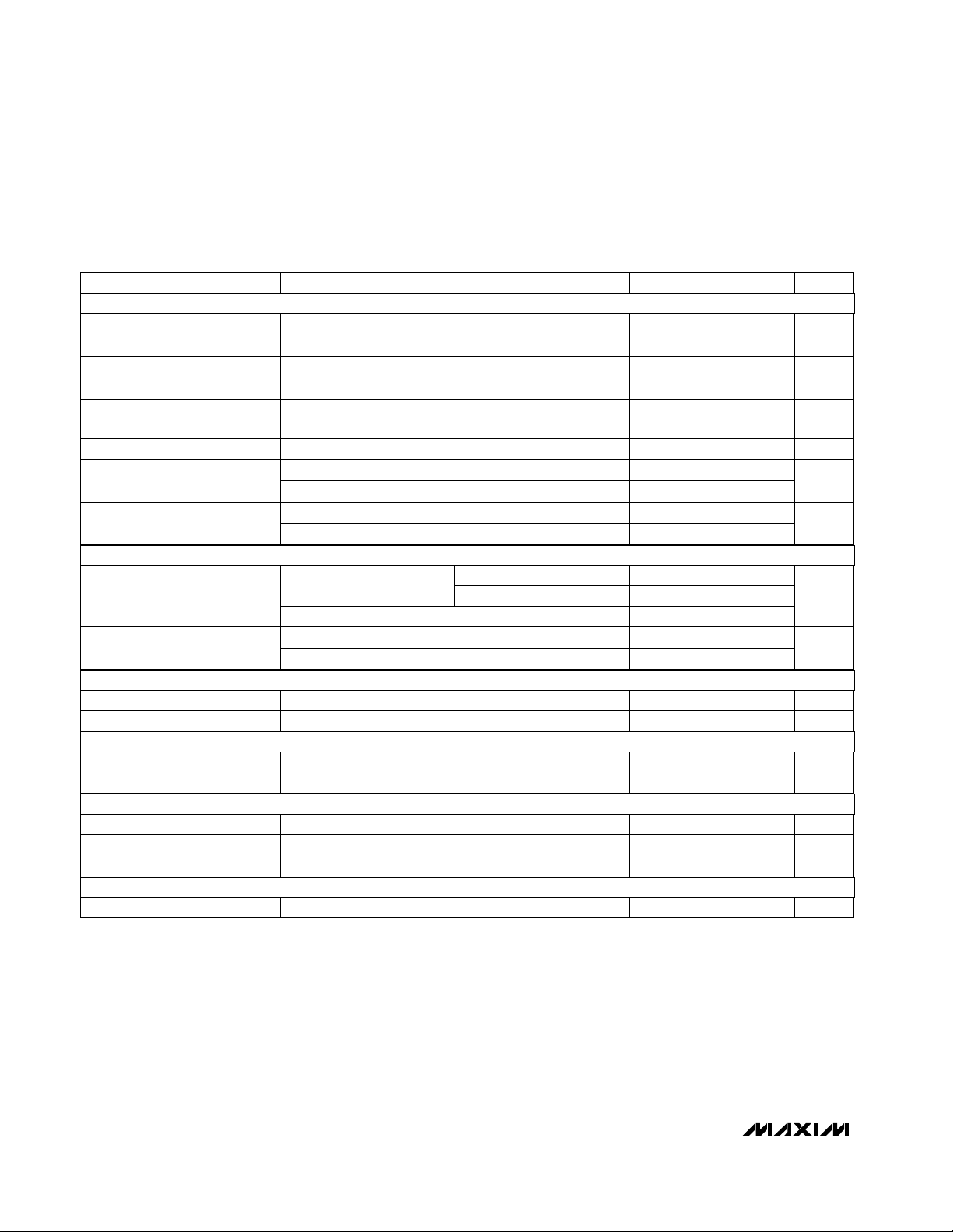
ELECTRICAL CHARACTERISTICS (continued)
(CLK/SEL = ONA = ONB = FB = PGND = GND, OUT = POUT, V
OUT
= 3.6V (Note 6); MAX1701: AIN = LBN = GND, LBP = REF,
T
A
= -40°C to +85°C, unless otherwise noted.) (Note 8)
LBP falling, 15mV hysteresis
Rising V
FB
Adjustable output, CLK/SEL = OUT, V
BATT
= 2.4V,
includes load regulation error for 0A ≤ I
LX
≤ 0.55A
10µA < IAO< 100µA
IAO= 20µA
VFB< 0.1V, CLK/SEL = OUT, V
BATT
= 2.4V, includes load
regulation error for 0A ≤ I
LX
≤ 0.55A
CLK/SEL = OUT
Rising V
OUT
, VFB< 0.1V
P-channel
N-channel
V
(Note 4)
V
ONB
= 3.6V
CLK/SEL = GND (MAX1700)
2.92 3.03
CLK/SEL = OUT (MAX1700)
Internal Trip Level
CONDITIONS
mV-5 5LBN, LBP Input Offset
V1.1 1.14External Trip Level
mmho516Transconductance
V1.23 1.27
To maintain input offset < ±5mV (at least one input must
be within this range)
AIN Reference Voltage
mA
250 600
N-Channel Current Limit
1100 1800
V0.5 1.5
LBN, LBP Common Mode
Range
I
REF
= 0 V1.23 1.27Reference Output Voltage
V1.20 1.27FB Regulation Voltage
V3.17 3.38Output Voltage (Note 3)
Ω
0.5
Switch On-Resistance
0.28
0.45
V2.0 2.3
Output Voltage Lockout
Threshold
µA20Supply Current in Shutdown
µA
70
Supply Current in Low-Power
Mode (Note 6)
µA
250
Supply Current in Low-Noise
Mode (Note 6)
UNITSMIN TYP MAXPARAMETER
CLK/SEL = GND (MAX1701)
CLK/SEL = OUT (MAX1701)
CLK/SEL = GND
CLK/SEL = OUT
CLK/SEL = GND
110
300
DC-DC CONVERTER
DC-DC SWITCHES
GAIN BLOCK (MAX1701)
POWER-GOOD (MAX1701)
LOW-BATTERY COMPARATOR (MAX1701)
REFERENCE
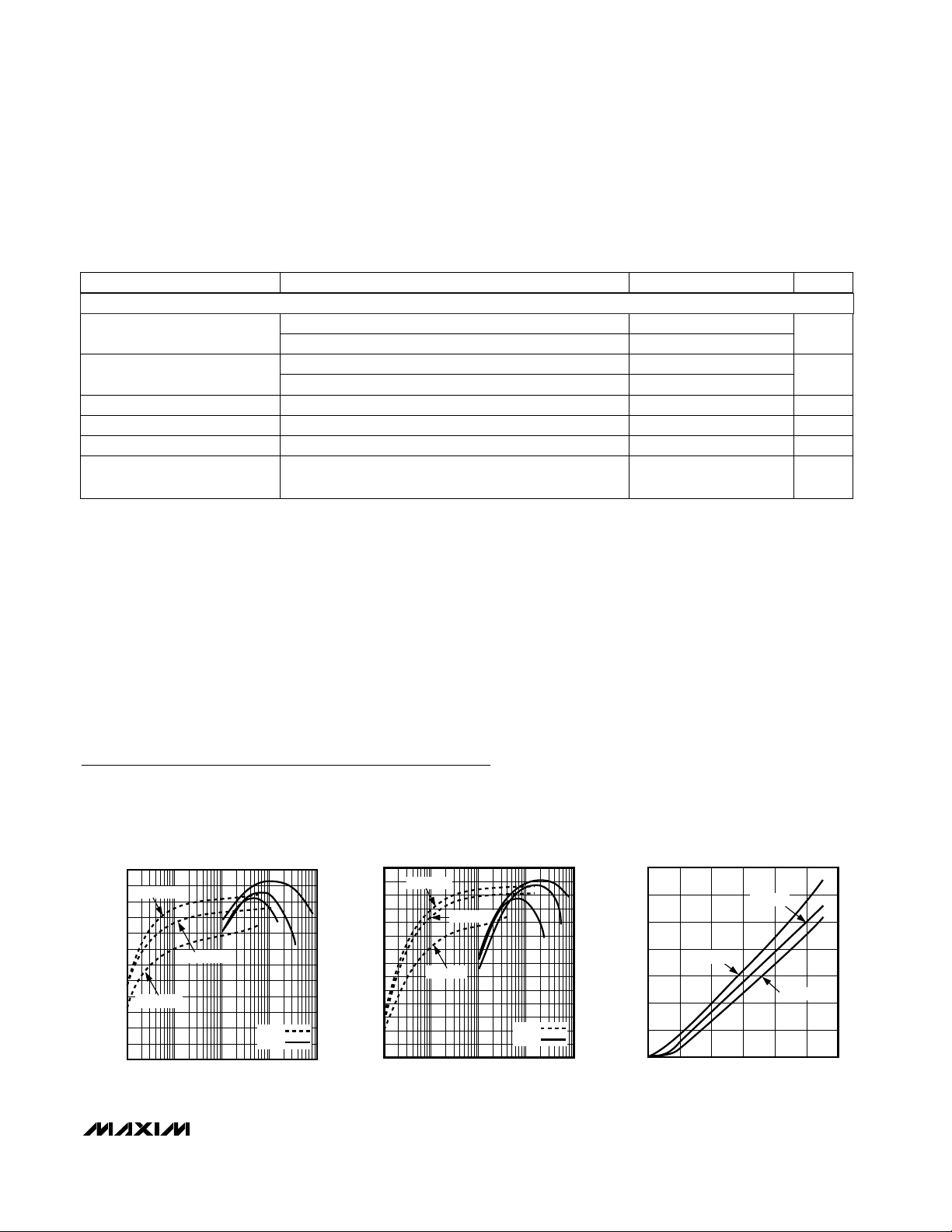
Input High Voltage (Note 7)
MAX1700/MAX1701
1-Cell to 3-Cell, High-Power (1A),
Low-Noise, Step-Up DC-DC Converters
_______________________________________________________________________________________ 5
Note 1: Operating voltage. Since the regulator is bootstrapped to the output, once started it will operate down to 0.7V input.
Note 2: Start-up is tested with the circuit of Figure 2.
Note 3: In low-power mode (CLK/SEL = GND), the output voltage regulates 1% higher than low-noise mode (CLK/SEL = OUT or
synchronized).
Note 4: The regulator is in start-up mode until this voltage is reached. Do not apply full load current.
Note 5: Load regulation is measured from no-load to full load where full load is determined by the N-channel switch current limit.
Note 6: Supply current from the 3.30V output is measured between the 3.30V output and the OUT pin. This current correlates
directly to the actual battery supply current, but is reduced in value according to the step-up ratio and efficiency. Set V
OUT
= 3.6V to keep the internal switch open when measuring the current into the device.
Note 7: ONA and ONB have hysteresis of approximately 0.15xV
OUT
.
Note 8: Specifications to -40°C are guaranteed by design and not production tested.
ELECTRICAL CHARACTERISTICS (continued)
(CLK/SEL = ONA = ONB = FB = PGND = GND, OUT = POUT, V
OUT
= 3.6V, MAX1701: AIN = LBN = GND, LBP = REF,
T
A
= -40°C to +85°C, unless otherwise noted.) (Note 8)
CONDITIONS
2.5V < V
OUT
< 5.5V, CLK/SEL
1.2V < V
OUT
< 5.5V, ONA and ONB
0.2V
OUT
V
0.2V
OUT
Input Low Voltage (Note 7)
1.2V < V
OUT
< 5.5V, ONA and ONB
0.8V
OUT
Input High Voltage (Note 7)
ONA, ONB, and CLK/SEL
2.5V < V
OUT
< 5.5V, CLK/SEL
µA-1 1Logic Input Current
V
0.8V
OUT
CLK/SEL = OUT kHz260 340Internal Oscillator Frequency
UNITSMIN TYP MAXPARAMETER
%80 92Oscillator Maximum Duty Cycle
kHz200 400
External Clock Frequency
Range
Typical Operating Characteristics
(TA = +25°C, unless otherwise noted.)
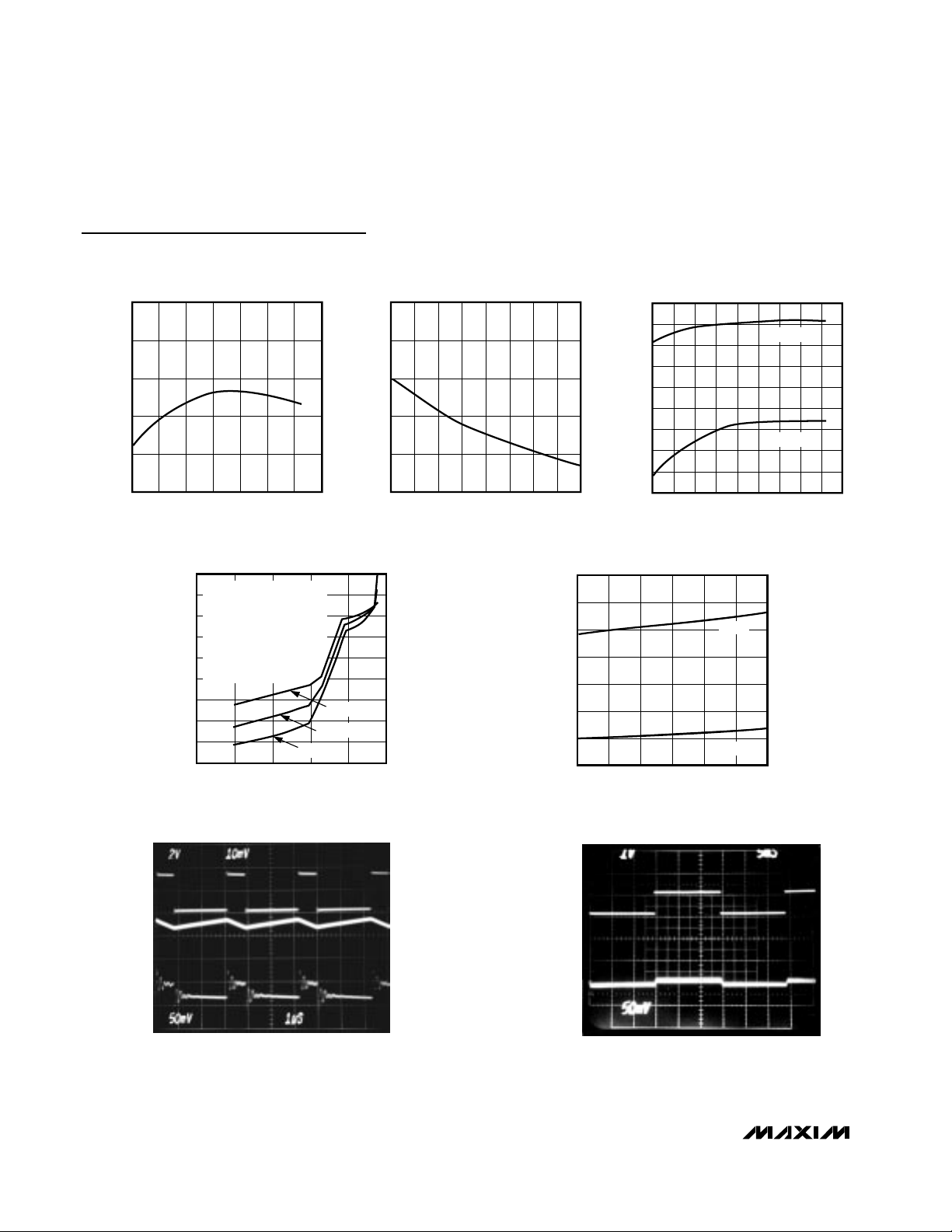
100
90
40
0.1 1 10 100 1000
EFFICIENCY vs. LOAD CURRENT
(V
OUT
= 3.3V)
50
MAX1700-01
LOAD CURRENT (mA)
EFFICIENCY (%)
60
70
80
PFM
PWM
VIN = 0.9V
VIN = 1.2V
VIN = 2.4V
MAX1700-02
100
90
40
30
0.1 1 10 100 1000
EFFICIENCY vs. LOAD CURRENT
(V
OUT
= 5V)
50
LOAD CURRENT (mA)
EFFICIENCY (%)
60
70
80
VIN = 1.2V
VIN = 2.4V
VIN = 3.6V
PFM
PWM
0
2.0
1.0
4.0
3.0
6.0
5.0
7.0
0231 456
MAX1701
SHUTDOWN CURRENT
vs. INPUT VOLTAGE (V)
MAX1770-03
INPUT VOLTAGE (V)
SHUTDOWN CURRENT (µA)
T = 85°C
T = 25°C
T = -40°C
LOGIC AND CONTROL INPUTS
MAX1700/MAX1701
1-Cell to 3-Cell, High-Power (1A),
Low-Noise, Step-Up DC-DC Converters
6 _______________________________________________________________________________________
Typical Operating Characteristics (continued)
(TA = +25°C, unless otherwise noted.)
1.244
1.246
1.250
1.248
1.252
1.254
-40 0-20 20 40 60 80 100
REFERENCE VOLTAGE
vs. TEMPERATURE
MAX1700-04
TEMPERATURE (°C)
REFERENCE VOLTAGE (V)
1.244
1.246
1.250
1.248
1.252
1.254
0203010 40 50 60 70 80
REFERENCE VOLTAGE
vs. REFERENCE CURRENT
MAX1700-05
REFERENCE CURRENT (µA)
REFERENCE VOLTAGE (V)
0.2
0.6
0.4
1.0
0.8
1.4
1.2
1.6
2.5 3.5 43 4.5 5 5.5
PEAK INDUCTOR CURRENT
vs. OUTPUT VOLTAGE
MAX1700-08
OUTPUT VOLTAGE (V)
CURRENT LIMIT (A)
PFM
PWM
280
290
285
305
300
295
315
320
310
325
-40 20 40-20 0 60 80 100 120 140
FREQUENCY vs. TEMPERATURE
MAX1700-06
TEMPERATURE (°C)
FREQUENCY (kHz)
V
OUT
= 5V
V
OUT
= 3.3V
I
OUT
= 0mA, V
OUT
= 3.3V
A = V
IN
, 1.1V TO 2.1V, 1V/div
B = V
OUT
RIPPLE, 50mV/div, AC COUPLED
LINE-TRANSIENT RESPONSE
A
B
0V
5ms/div
MAX1700-09
VIN = 1.1V, I
OUT
= 200mA, V
OUT
= 3.3V
A = LX VOLTAGE, 2V/div
B = INDUCTOR CURRENT, 0.5A/div
C = V
OUT
RIPPLE, 50mV/div, AC COUPLED
HEAVY-LOAD SWITCHING WAVEFORMS
(V
OUT
= 3.3V)
A
B
C
0A
0V
V
OUT
1µs/div
MAX1700-08
0.5
0.01
START-UP INPUT VOLTAGE
vs. OUTPUT CURRENT
0.9
0.7
1.1
MAX1700/01 TOC06a
OUTPUT CURRENT (mA)
START-UP INPUT VOLTAGE (V)
100
1.7
1.5
2.1
1.9
1.3
0.1 10 1000
2.3
1
NO-LOAD START-UP:
1.0V AT -40°C
0.79 AT +25°C
0.64V AT +85°C
CONSTANT-CURRENT LOAD
V
OUT
= 3.3V
L = 10µH
D1 = MBR0520L
TA = -40°C
TA = +25°C
TA = +85°C

MAX1700/MAX1701
1-Cell to 3-Cell, High-Power (1A),
Low-Noise, Step-Up DC-DC Converters
_______________________________________________________________________________________ 7
VIN = 1.2V, V
OUT
= 3.3V, C
OUT
= 440µF
A = V
OUT
RIPPLE, 200mV/div, AC COUPLED
B = LOAD CURRENT, 50mA TO 400mA, 0.2A/div,
PULSE WIDTH = 416µs
DECT LOAD-TRANSIENT RESPONSE
A
B
3.3V
0A
2ms/div
MAX1700-13
Typical Operating Characteristics (continued)
(Circuit of Figure 1, TA= +25°C, unless otherwise noted.)
2.7
0.1k 1k 10k 100k 1M
NOISE SPECTRUM
(V
OUT
= 3.3V, VIN = 1.2V, R
LOAD
= 50Ω)
0
MAX1700-14
FREQUENCY (Hz)
NOISE (mV
RMS
)
A = V
ON1
, 2V/div
B = V
OUT
, 1V/div
C = INPUT CURRENT, 0.2A/div
POWER-ON DELAY
(PFM MODE)
A
B
C
0mA
3.3V
5ms/div
MAX1700-11
VIN = 3.6V, V
OUT
= 5V, C
OUT
= 440µF
A = V
OUT
RIPPLE, 200mV/div, AC COUPLED
B = LOAD CURRENT, 100mA TO 1A, 0.5A/div,
PULSE WIDTH = 577µs
GSM LOAD-TRANSIENT RESPONSE
A
5V
0A
B
1ms/div
MAX1700-12
VIN = 1.1V, V
OUT
= 3.3V
A = LOAD CURRENT, 0mA TO 200mA, 0.2A/div
B = V
OUT
RIPPLE, 50mV/div, AC COUPLED
LOAD-TRANSIENT RESPONSE
A
B
0A
200mA
2ms/div
MAX1700-10

MAX1700/MAX1701
1-Cell to 3-Cell, High-Power (1A),
Low-Noise, Step-Up DC-DC Converters
8 _______________________________________________________________________________________
Pin Description
1 Low-Battery Comparator Non-Inverting InputLBP—
2 Low-Battery Comparator Inverting InputLBN—
3
Reference Output. Bypass with a 0.22µF capacitor to GND. REF can source up to
50µA.
REF3
4
Switching-Mode Selection and External-Clock Synchronization Inputs.
• CLK/SEL=Low: Low-power, delivers up to 10% of full load current.
• CLK/SEL=High: High-power PWM mode. Full output power available. Operates in
low-noise, constant-frequency mode.
• CLK/SEL=External Clock: High-power PWM mode with the internal oscillator
synchronized to the external clock.
Turning on with CLK/SEL=0V also serves as a soft-start function since peak inductor
current is limited to 25% of that allowed in PWM mode.
CLK/SEL4
5 GroundGND5
6
Power-Okay Comparator Output. Open drain N-channel output is low when V
OUT
is
10% below regulation point. No internal delay is provided.
POK—
7
Shutdown Input. When ONB =high and ONA=low, the IC is off and the load is connected to the battery through the Schottky diode.
ONB
7
8
Turn ON Input. When ONA=high or ONB =low, the IC turns on.
ONA8
9 Gain Block Output. This open-drain output sinks when V
AIN<VREF
.AO—
10
Gain Block AIN input. When AIN is low, AO sinks current. The transconductance from
AIN to AO is 9mmhos.
AIN—
11
DC-DC Converter Dual-Mode Feedback Input. For a fixed output voltage of +3.3V,
connect FB to GND. For adjustable output, connect a divider between POUT and GND
to set the output voltage in the range of 2.5V to 5V.
FB11
12 Source of N-Channel Power MOSFET Switch. Connect to high-current ground path.PGND12
13 Drain of P-Channel Synchronous Rectifier and N-Channel SwitchLX13
14 Output Sense Input. Power source for the IC.OUT14
15
Source of P-Channel Synchronous Rectifier MOSFET Switch. Connect an external
Schottky diode from LX to POUT.
POUT15
16
Low-Battery Comparator Output. Open-drain N-channel output is low when LBN > LBP
Input hysteresis is 15mV.
LBO—
PIN
MAX1701MAX1700
FUNCTIONNAME
— Internal Connection. Leave open or connect to GND.I.C.
1, 2, 6, 9,
10, 16

MAX1700/MAX1701
1-Cell to 3-Cell, High-Power (1A),
Low-Noise, Step-Up DC-DC Converters
_______________________________________________________________________________________ 9
_______________Detailed Description
The MAX1700/MAX1701 are highly efficient, low-noise
power supplies for portable RF and data acquisition
instruments. The MAX1700 combines a boost switching
regulator, N-channel power MOSFET, P-channel synchronous rectifier, precision reference, and shutdown
control. The MAX1701 contains all of the MAX1700 features plus a versatile gain amplifier, POK output, and a
low-battery comparator (Figure 1). The MAX1700/
MAX1701 come in a 16-pin QSOP package, which
occupies no more space than an 8-pin SO.
The switching DC-DC converter boosts a 1- to 3-cell
input to an adjustable output between 2.5V and 5.5V.
The MAX1700/MAX1701 start from a low 1.1V input and
remain operational down to 0.7V.
These devices are optimized for use in cellular phones
and other applications requiring low noise during full-
power operation, as well as low-quiescent current for
maximum battery life during standby and shutdown
modes. They feature constant-frequency (300kHz), lownoise PWM operation with up to 800mA output capability. See Table 1 for typical available output current. A
low-quiescent-current, low-power mode offers an output up to 100mA and reduces quiescent power consumption to 200µW. In shutdown mode, the quiescent
current is further reduced to just 3µA. Figure 2 shows
the standard application circuit for the
MAX1700/MAX1701.
Additional features include synchronous rectification for
high efficiency and improved battery life, a POK output,
and an uncommitted comparator for low-battery detection (MAX1701). A CLK input allows frequency synchronization to reduce interference. Dual shutdown controls
allow shutdown using a momentary pushbutton switch
and microprocessor control (MAX1701).
2.25V
IC PWR
1.25V
FEEDBACK AND
POWER-GOOD
SELECT
REFERENCE
UNDERVOLTAGE LOCKOUT
COMPARATOR
GAIN
BLOCK
FEEDBACK
START-UP
OSCILLATOR
OSCILLATOR
300kHz
PFM/PWM
CONTROLLER
PFM/PWM
PCH
0.25Ω
NCH
0.13Ω
REF
EN
D
EN
POUT
LX
PGND
POK*
AO*
LBO*
N
N
N
OSC
MODE
FB
EN
Q
Q
Q
*MAX1701 ONLY
LBP*
LBN*
ONA
REF
FB
GND
CLK/SEL
ON
RDY
REF
AIN*
ONB
OUT
Figure 1. Functional Diagram

MAX1700/MAX1701
Step-Up Converter
The step-up switching DC-DC converter generates an
adjustable output from 2.5V to 5.5V. During the first part
of each cycle, the internal N-channel MOSFET switch is
turned on. This allows current to ramp up in the inductor and store energy in a magnetic field. During the
second part of each cycle, when the MOSFET is turned
off, the voltage across the inductor reverses and forces
current through the diode and synchronous rectifier to
the output filter capacitor and load. As the energy
stored in the inductor is depleted, the current ramps
down and the output diode and synchronous rectifier
turn off. Voltage across the load is regulated using
either low-noise PWM or low-power operation, depending on the CLK/SEL pin setting (Table 2).
Low-Noise PWM Operation
When CLK/SEL is pulled high, the MAX1700/MAX1701
operate in a higher power, low-noise pulse-widthmodulation (PWM) mode. During PWM operation, they
switch at a constant frequency (300kHz) and then modulate the MOSFET switch pulse width to control the
power transferred per cycle and regulate the voltage
across the load. In PWM mode the devices can output
up to 800mA. Switching harmonics generated by fixedfrequency operation are consistent and easily filtered.
See the Noise Spectrum Plot in the
Typical Operating
Characteristics.
During PWM operation, each rising edge of the internal
clock sets a flip-flop, which turns on the N-channel
MOSFET switch (Figure 3). The switch is turned off
when the sum of the voltage-error, slope compensation,
and current-feedback signals trips a multi-input comparator and resets the flip-flop; the switch remains off
for the rest of the cycle. When a change occurs in the
output-voltage error signal into the comparator, it shifts
the level to which the inductor current is allowed to
ramp during each cycle and modulates the MOSFET
switch pulse width. A second comparator enforces an
inductor current limit of 1.6A max.
1-Cell to 3-Cell, High-Power (1A),
Low-Noise, Step-Up DC-DC Converters
10 ______________________________________________________________________________________
PGNDGND
FB
POUT
OUT
LX
D1
OUTPUT
OUT
FIXED
OUTPUT
(GND)
MBR0520L
2 x
100µF
ADJUSTABLE
L1 10µH
REF
CLK/SEL
ONA
ONB
R2
R1
0.22µF
0.22µF
0.22µF
22µF
10Ω
0.7V TO 5.5V
MAX1700
MAX1701
Figure 2. Fixed or Adjustable Output (PWM mode).
CLK/SEL MODE FEATURES
0 Low Power Low supply current
1 PWM
Low noise,
high output current
External Clock
(200kHz to 400kHz)
Synchronized
PWM
Low noise,
high output current
Table 2. Selecting the Operating Mode
Table 1. Typical Available Output Current
POUT
LX
PGND
P
N
S
Q
R
FB
REF
1.3A CURRENT
LIMIT
OSC
Figure 3. Simplified PWM Controller Block Diagram
NUMBER
OF CELLS
INPUT
VOLTAGE (V)
OUTPUT
CURRENT (mA)
1 NiCd/NiMH 1.2 300
2 NiCd/NiMH 2.4 750
2 NiCd/NiMH 2.4 525
OUTPUT
VOLTAGE (V)
3.3
3.3
5.0
3 NiCd/NiMH
or 1 Li-Ion
3.6 8505.0

Synchronized PWM Operation
By applying an external clock to CLK/SEL, the
MAX1700/MAX1701 can also be synchronized in PWM
mode to a frequency between 200kHz and 400kHz.
This allows the user to set the harmonics to avoid IF
bands in wireless applications. The synchronous rectifier is also active during synchronized PWM operation.
Low-Power PFM Operation
Pulling CLK/SEL low places the MAX1700/MAX1701 in
a low-power mode. During low-power mode, PFM operation regulates the output voltage by transferring a
fixed amount of energy during each cycle and then
modulating the switching frequency to control the
power delivered to the output. The devices switch only
as needed to service the load, resulting in the highest
possible efficiency at light loads. Output current capability in PFM mode is 100mA. The output voltage is typically 1% higher than the output voltage in PWM mode.
During PFM operation, the error comparator detects the
output voltage falling out of regulation and sets a flipflop, turning on the N-channel MOSFET switch (Figure
4). When the inductor current ramps to the PFM mode
current limit (400mA typical) and stores a fixed amount
of energy, the current-sense comparator resets a flipflop. The flip-flop turns off the N-channel switch and
turns on the P-channel synchronous rectifier. A second
flip-flop, previously reset by the switch’s “on” signal,
inhibits the error comparator from initiating another
cycle until the energy stored in the inductor is transferred to the output filter capacitor and the synchronous
rectifier current has ramped down to 70mA. This forces
operation with a discontinuous inductor current.
Synchronous Rectifier
The MAX1700/MAX1701 feature an internal 250mΩ, Pchannel synchronous rectifier to enhance efficiency.
Synchronous rectification provides a 5% efficiency
improvement over similar nonsynchronous boost regulators. In PWM mode, the synchronous rectifier is
turned on during the second half of each switching
cycle. In low-power mode, an internal comparator turns
on the synchronous rectifier when the voltage at LX
exceeds the boost-regulator output and then turns it off
when the inductor current drops below 70mA.
Low-Voltage Start-Up Oscillator
The MAX1700/MAX1701 use a CMOS, low-voltage
start-up oscillator for a 1.1V guaranteed minimum startup input voltage at +25°C. On start-up, the low-voltage
oscillator switches the N-channel MOSFET until the output voltage reaches 2.15V. Above this level, the normal
boost-converter feedback and control circuitry take
over. Once the device is in regulation, it can operate
down to a 0.7V input since internal power for the IC is
bootstrapped from the output using the OUT pin. Do
not apply full load until the output exceeds 2.4V.
Shutdown
The MAX1700/MAX1701 shut down to reduce quiescent current to typically 3µA. During shutdown, the reference, low-battery comparator, gain block, and all
feedback and control circuitry are off. The boost converter’s output drops to one Schottky diode drop below
the input.
Table 3 shows the control logic with ONA and ONB.
Both inputs have trip points near 0.5V
OUT
with
0.15V
OUT
hysteresis.
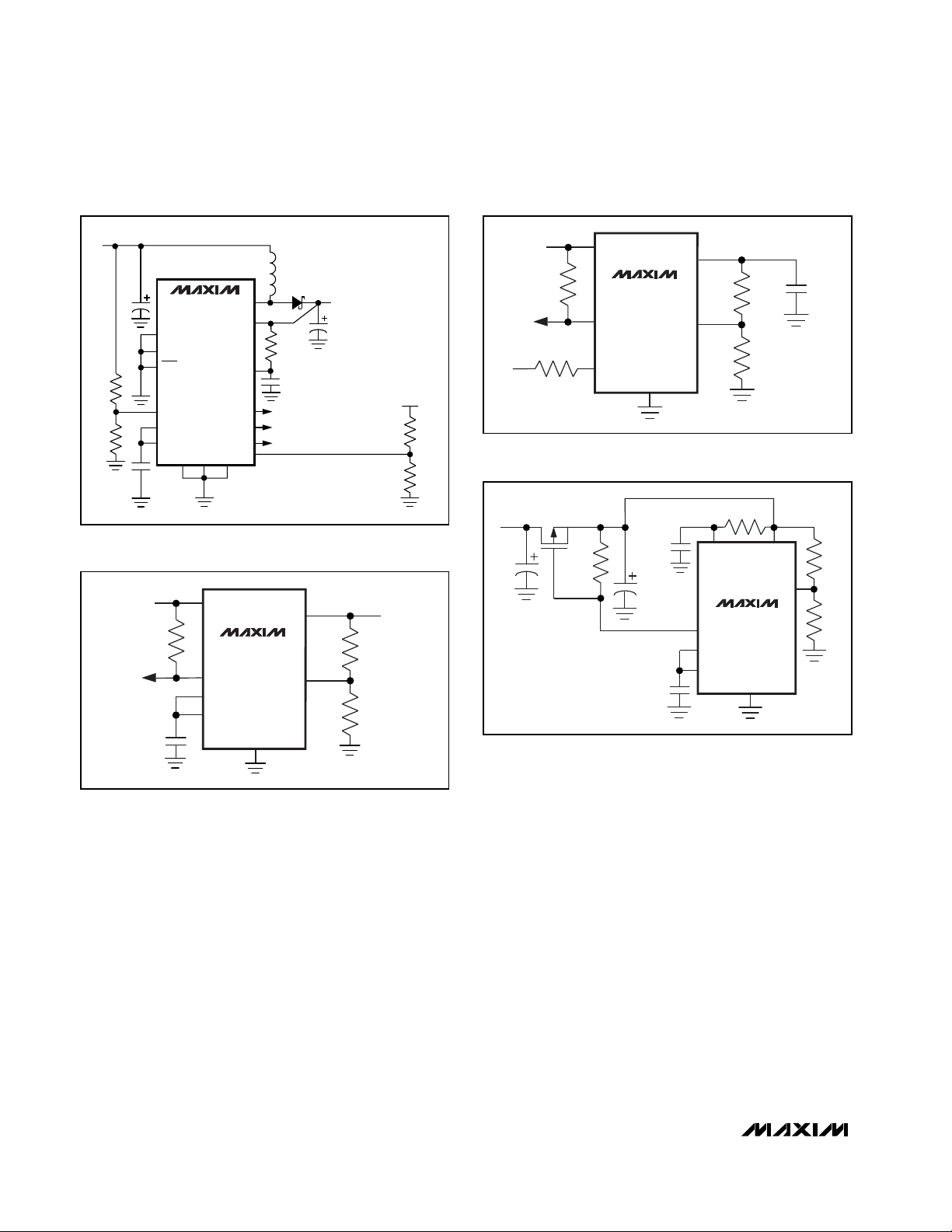
Low-Battery Comparator (MAX1701)
The internal low-battery comparator has uncommitted
inputs and an open-drain output (LBO) capable of sinking 1mA. To use it as a low-battery-detection comparator, connect the LBN input to the reference, and
connect the LBP input to an external resistor divider
MAX1700/MAX1701
1-Cell to 3-Cell, High-Power (1A),
Low-Noise, Step-Up DC-DC Converters
______________________________________________________________________________________ 11
N
LX
PGND
FB
REF
400mA
CURRENT
LIMIT
ERROR
COMPARATOR
SQ
R
Q
Q
R
D
LOGIC HIGH
POUT
P
Figure 4. Controller Block Diagram in Low-Power PFM Mode
ONA
OONNBB
Status
0 0 On
0 1 Off
1 0 On
1 1 On
Table 3. On/Off Logic Control
MAX1700/MAX1701
between the positive battery terminal and GND (Figure
5). The resistor values are then calculated as follows:
R3 = R4(VTH/V
LBN
-1)
where VTHis the desired input voltage trip threshold
and V
LBN
= V
REF
= 1.25V. Since the input bias current
into LBP is less than 20nA, R4 can be a large value
(such as 270kΩ or less) without sacrificing accuracy.
The inputs have a common-mode input range from
0.5V to 1.5V and an input-referred hysteresis of 15mV.
The low-battery comparator can also be used to moni-
tor the output voltage, as shown in Figure 6.
To set the low-battery threshold to a voltage below the
1.25V reference, insert a resistor divider between REF
and LBN and connect the battery to the LBP input
through a 10kΩ current-limiting resistor (Figure 7). The
equation for setting the resistors for the low-battery
threshold is then as follows:
R5 = R6(V
REF/VLBP
-1)
where V
LBP
is the desired voltage threshold. In Figures
5, 6, and 7, LBO goes low for a low-voltage input. The
low-battery comparator can be used to check the output voltage or to control the load directly on P
OUT
during start-up (Figure 8). Use the following equation to set
the resistor values:
R3 = R4(V
OUTTH/VLBP
- 1)
where V
OUTTH
is the desired output-voltage trip point
and V
LBP
is connected to the reference or 1.25V.
1-Cell to 3-Cell, High-Power (1A),
Low-Noise, Step-Up DC-DC Converters
12 ______________________________________________________________________________________
FBPGNDGND
AO ARBITRARY VOLTAGE MONITOR
ARBITRARY
VOLTAGE
LOW-BATTERY MONITOR
VOLTAGE MONITOR
AIN
LBO
POK
OUT
POUT
LX
D1
L1
LBP
LBN
REF
CLK/SEL
ONA
ONB
R4
R6
R5
R3
10Ω
0.22µF
0.7V TO 5.5V
MAX1701
Figure 5. Detecting Battery Voltage Above 1.25V
MAX1701
LBN
LBO
LBP
POUT
REF
GND
R5
R6
BATTERY
VOLTAGE
10k
0.22µF
Figure 6. Using the Low-Battery Comparator to Sense the
Output Voltage (MAX1701)
Figure 7. Detecting Battery Voltages Below 1.25V (MAX1701)
270k
MAX1701
LBP
LBO
LBN
0.22µF
OUT
POUT
10Ω
REF
GND
R3
R4
P
C3
0.22µF
C4
C5
OUTPUT
Figure 8. Using the Low-Battery Comparator for Load Control
During Start-Up
POUT
MAX1701
LBO
LBN
REF
0.22µF
OUT
R3
LBP
R4
GND
Reference
The MAX1700/MAX1701 have an internal 1.250V, 1%
bandgap reference. Connect a 0.22µF bypass capacitor to GND within 0.2in. (5mm) of the REF pin. REF can
source up to 50µA of external load current.
Power-OK (MAX1701)
The MAX1701 features a power-good comparator. This
comparator’s open-drain output (POK) is pulled low
when the output voltage falls to 10% below the regulation point.
Gain Block (MAX1701)
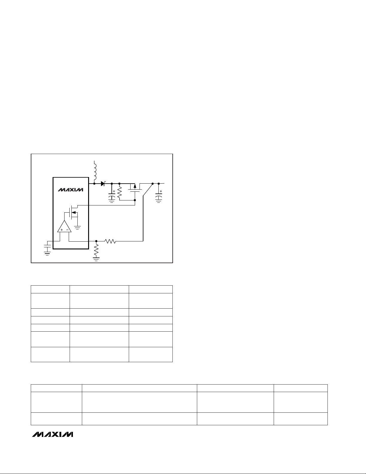
The MAX1701’s gain block can function as a third comparator or can be used to build a linear regulator using
an external P-channel MOSFET pass device. The gainblock output is a single-stage transconductance amplifier that drives an open-drain N-channel MOSFET.
Figure 9 shows the gain block used in a linear regulator. The output of an external P-channel pass element is
compared to the internal reference. The difference is
amplified and used to drive the gate of the pass element. Use a logic-level PFET such as the Fairchild
NDS336P (R
DS(ON)
= 270mΩ). If the PFET R
DS(ON)
is
less than 250mΩ, the linear regulator output filter
capacitance may need to be increased to above 47µF.
__________________Design Procedure
Setting the Output Voltages
Set the output voltage between 2.5V and 5.5V by connecting a resistor voltage-divider to FB from OUT to
GND, as shown in Figure 2. The resistor values are then
as follows:
R1 = R2 (V
OUT/VFB
- 1)
where V
FB
, the boost-regulator feedback setpoint, is
1.23V. Since the input bias current into FB is less than
20nA, R2 can have a large value (such as 270kΩ or
less) without sacrificing accuracy. Connect the resistor
voltage-divider as close to the IC as possible, within
0.2in. (5mm) of the FB pin.
Inductor Selection
The MAX1700/MAX1701’s high switching frequency
allows the use of a small surface-mount inductor. A
10µH inductor should have a saturation-current rating
that exceeds the N-channel switch current limit of 1.6A.
However, it is generally acceptable to bias the inductor
current into saturation by as much as 20%, although
this will slightly reduce efficiency. For high efficiency,
choose an inductor with a high-frequency core material
(such as ferrite) to reduce core losses. To minimize
radiated noise, use a toroid, pot core, or shielded bobbin inductor. Connect the inductor from the battery to
the LX pin as close to the IC as possible. See Table 4
for a list of component suppliers and Table 5 for suggested components.
MAX1700/MAX1701
1-Cell to 3-Cell, High-Power (1A),
Low-Noise, Step-Up DC-DC Converters
______________________________________________________________________________________ 13
AIN
AO
N
LX
P
IN
REF
R6
R5
2x
100µF
47µF
MAX1701
20k
Figure 9. Using Gain Block as a Linear Regulator
PRODUCTION INDUCTORS CAPACITORS DIODES
Surface Mount
Sumida CDR63B, CD73, CDR73B, CD74B series
Coilcraft DO1608, DO3308, DT3316 series
Matsuo 267 series
Sprague 595D series
AVX TPS series
Motorola MBR0520L
Through Hole Sumida RCH654 series
Sanyo OS-CON series
Nichicon PL series
1N5817
Table 5. Component Selection Guide
(847) 956-0702
81-3-3607-5144
USA: (847) 956-0666
Japan: 81-3-3607-5111
Sumida
(619) 661-1055
81-7-2070-1174
USA: (619) 661-6835
Japan: 81-7-2070-6306
Sanyo
(602) 994-6430USA: (602) 303-5454Motorola
(714) 960-6492USA: (714) 969-2491Matsuo
(847) 639-1469USA: (847) 639-6400Coilcraft
(803) 626-3123USA: (803) 946-0690
(800) 282-4975
AVX
FAXPHONESUPPLIER
Table 4. Component Suppliers

MAX1700/MAX1701
Output Diode
Use a Schottky diode, such as a 1N5817, MBR0520L, or
equivalent. The Schottky diode carries current during
start-up, and in PFM mode after the synchronous rectifier
turns off. Thus, its current rating only needs to be 500mA.
Connect the diode between LX and P
OUT
as close to the
IC as possible. Do not use ordinary rectifier diodes since
slow switching speeds and long reverse recovery times
will compromise efficiency and load regulation.
Input and Output Filter Capacitors
Choose input and output filter capacitors that will service the input and output peak currents with acceptable voltage ripple. Choose input capacitors with
working voltage ratings over the maximum input voltage, and output capacitors with working voltage ratings
higher than the output.
For full output, two 100µF, 100mΩ, low-ESR tantalum output filter capacitors are recommended. For loads below
250mA, a single 100µF output capacitor will suffice. The
input filter capacitor (CIN) reduces peak currents drawn
from the input source and reduces input switching noise.
The input voltage source impedance determines the
required size of the input capacitor. When operating
directly from one or two NiCd cells placed close to the
MAX1700/MAX1701, use a 22µF, low-ESR input filter
capacitor. When operating from a power source placed
farther away, or from higher impedance batteries such as
alkaline or lithium cells, use one or two 100µF, 100mΩ,
low-ESR tantalum capacitors.
Sanyo OS-CON and Panasonic SP/CB-series ceramic
capacitors offer the lowest ESR. Low-ESR tantalum
capacitors are a good choice and generally offer a
good tradeoff between price and performance. Do not
exceed the ripple current ratings of tantalum capacitors. Avoid most aluminum-electrolytic capacitors,
since their ESR is often too high.
Bypass Capacitors
Two ceramic bypass capacitors are required for proper
operation. Bypass REF with a 0.22µF capacitor to GND.
Also connect a 0.22µF ceramic capacitor from OUT to
GND. Each should be placed as close to their respective pins as possible, within 0.2in. (5mm) of the DC-DC
converter IC. See Table 4 for suggested suppliers.
__________Applications Information
Push-On/Push-Off Control
A momentary pushbutton switch can be used to turn
the MAX1700/MAX1701 on and off. In Figure 10, ONA
is pulled low and ONB is pulled high when the part is
off. When the momentary switch is pressed, ONB is
pulled low and the regulator turns on. The switch must
be pressed long enough for the microcontroller to exit
reset (200ms) and drive ONA high. A small capacitor is
added to help debounce the switch. The controller
issues a logic high to ONA, which holds the part on
regardless of the switch state. To turn the regulator off,
press the switch again, allowing the controller to read
the switch status and pull ONA low. When the switch is
released, ONB is pulled high.
Use in a Typical Wireless
Phone Application
The MAX1700/MAX1701 are ideal for use in digital
cordless and PCS phones. The power amplifier (PA) is
connected directly to the boost-converter output for
maximum voltage swing (Figure 11). Low-dropout linear
regulators are used for post-regulation to generate
1-Cell to 3-Cell, High-Power (1A),
Low-Noise, Step-Up DC-DC Converters
14 ______________________________________________________________________________________
µC
V
DD
I/O
MAX1701
ONA
ONB
OUT
I/O
0.1µF
ON/OFF
270k
270k
Figure 10. Momentary Pushbutton On/Off Switch
MAX1700
POUT
LX
MAX8865/MAX8866 DUAL OR
MAX8863/MAX8864 SINGLE
LOW-DROPOUT LINEAR REGULATORS
RADIOµC
PA
Figure 11. Typical Phone Application

low-noise power for DSP, control, and RF circuitry.
Typically, RF phones spend most of their life in standby
mode with only short periods in transmit/receive mode.
During standby, maximize battery life by setting
CLK/SEL = 0; this places the IC in low-power mode (for
the lowest quiescent power consumption).
Designing a PC Board
High switching frequencies and large peak currents
make PC board layout an important part of design.
Poor design can cause excessive EMI and groundbounce, both of which can cause instability or regulation errors by corrupting the voltage and current
feedback signals.
Power components (such as the inductor, converter IC,
filter capacitors, and output diode) should be placed as
close together as possible, and their traces should be
kept short, direct, and wide. A separate low-noise
ground plane containing the reference and signal
grounds should only connect to the power-ground
plane at one point. This minimizes the effect of powerground currents on the part. Consult the MAX1701 EV
kit manual for a layout example.
On multilayer boards, do not connect the ground pins
of the power components using vias through an internal
ground plane. Instead, place them close together and
route them in a star-ground configuration using component-side copper. Then use vias to connect the star
ground to the internal ground plane.
Keep the voltage feedback network very close to the
IC, within 0.2in. (5mm) of the FB pins. Keep noisy
traces, such as from the LX pin, away from the voltage
feedback networks. Separate them with grounded
copper. Consult the MAX1700 evaluation kit for a full
PC board example.
Soft-Start
To implement soft-start, set CLK/SEL low on power-up;
this forces low-power operation and reduces the peak
switching current to 550mA max. Once the circuit is in
regulation and start-up transients have settled,
CLK/SEL can be set high for full-power operation.
Intermittent Supply/Battery Connections
When boosting an input supply connected with a
mechanical switch, or a battery connected with spring
contacts, input power may sometimes be intermittent
as a result of contact bounce. When operating in PFM
mode with input voltages greater than 2.5V, restarting
after such dropouts may initiate high current pulses that
interfere with the MAX1700/MAX1701 internal MOSFET
switch control. If contact or switch bounce is anticipated in the design, use one of the following solutions.
1) Connect a capacitor (C
ONB
) from ONB to VIN, a 1MΩ
resistor (R
ONB
) from ONB to GND, and tie ONA to GND
(Figure 12). This RC network differentiates fast input
edges at VINand momentarily holds the IC off until V
IN
settles. The appropriate value of C
ONB
is 10-5times the
total output filter capacitance (C
OUT
), so a C
OUT
of
200µF results in C
ONB
= 2nF.
2) Use the system microcontroller to hold the
MAX1700/MAX1701 in shut down from the time when
power is applied (or reapplied) until the output capacitance (C
OUT
) has charged to at least the input voltage.
Power-on reset times of tens of milliseconds accomplish this.
3) Ensure that the IC operates, or at least powers up, in
PWM mode (CLK/SEL = high). Activate PFM mode only
after the V
OUT
has settled and all of the system’s power-
on reset flags are cleared.
MAX1700/MAX1701
1-Cell to 3-Cell, High-Power (1A),
Low-Noise, Step-Up DC-DC Converters
______________________________________________________________________________________ 15
16
15
14
13
12
11
10
9
1
2
3
4
5
6
7
8
LBP LBO
POUT
OUT
LX
PGND
FB
AIN
AO
MAX1701
QSOP
LBN
REF
POK
CLK/SEL
GND
ONB
ONA
TOP VIEW
Pin Configurations (continued)
Figure 12. Connecting C
ONB
and R
ONB
when Switch or
Battery-Contact Bounce Is Anticipated
POUT
OUT
LX
13
14
15
8
7
C
OUT
200µF
C
ONB
2nF
R
ONB
1M
ONA
ONB
MAX1700
MAX1701

MAX1700/MAX1701
1-Cell to 3-Cell, High-Power (1A),
Low-Noise, Step-Up DC-DC Converters
16 ______________________________________________________________________________________
________________________________________________________Package Information
QSOP.EPS
Chip Information
TRANSISTOR COUNT: 531
SUBSTRATE CONNECTED TO GND

 Loading...