

Page 1
General Description
The MAX17000 pulse-width modulation (PWM) controller provides a complete power solution for notebook
DDR, DDR2, and DDR3 memory. It comprises a stepdown controller, a source-sink LDO regulator, and a reference buffer to generate the required VDDQ, VTT, and
VTTR rails.
The VDDQ rail is supplied by a step-down converter
using Maxim’s proprietary Quick-PWM™ controller. The
high-efficiency, constant-on-time PWM controller handles wide input/output voltage ratios (low duty-cycle
applications) with ease and provides 100ns response
to load transients while maintaining a relatively constant
switching frequency. The Quick-PWM architecture circumvents the poor load-transient timing problems of
fixed-frequency current-mode PWMs while also avoiding the problems caused by widely varying switching
frequencies in conventional constant-on-time and constant-off-time PWM schemes. The controller senses the
current to achieve an accurate valley current-limit protection. It is also built in with overvoltage, undervoltage,
and thermal protections. The MAX17000 can be set to
run in three different modes: power-efficient SKIP
mode, low-noise forced-PWM mode, and standby
mode to support memory in notebook computer standby operation. The switching frequency is programmable from 200kHz to 600kHz to allow small components
and high efficiency. The VDDQ output voltage can be
set to a preset 1.8V or 1.5V, or be adjusted from 1.0V to
2.5V by an external resistor-divider. This output has 1%
accuracy over line-and-load operating range.
The MAX17000 includes a ±2A source-sink LDO regulator for the memory termination VTT rail. This VTT regulator has a ±5mV deadband that either sources or
sinks, ideal for the fast-changing load burst present in
memory termination applications. This feature also
reduces output capacitance requirements.
The VTTR reference buffer sources and sinks ±3mA,
providing the reference voltage needed by the memory
controller and devices on the memory bus.
The MAX17000 is available in a 24-pin, 4mm x 4mm,
Thin QFN package.
Applications
Notebook Computers
DDR, DDR2, and DDR3 Memory Supplies
SSTL Memory Supplies
Features
o SMPS Regulator (VDDQ)
Quick-PWM with 100ns Load-Step Response
Output Voltages—Preset 1.8V, 1.5V, or
Adjustable 1.0V to 2.5V
1% V
OUT
Accuracy Over Line and Load
26V Maximum Input Voltage Rating
Accurate Valley Current-Limit Protection
200kHz to 600kHz Switching Frequency
o Source/Sink Linear Regulator (VTT)
±2A Peak Source/Sink
Low-Output Capacitance Requirement
Output Voltages-Preset VDDQ/2 or REFIN
Adjustable from 0.5V to 1.5V
o Low Quiescent Current Standby State
o Soft-Start/Soft-Shutdown
o SMPS Power-Good Window Comparator
o VTT Power-Good Window Comparator
o Selectable Overvoltage Protection
o Undervoltage/Thermal Protections
o ±3mA Reference Buffer (VTTR)
MAX17000
Complete DDR2 and DDR3 Memory
Power-Management Solution
________________________________________________________________
Maxim Integrated Products
1
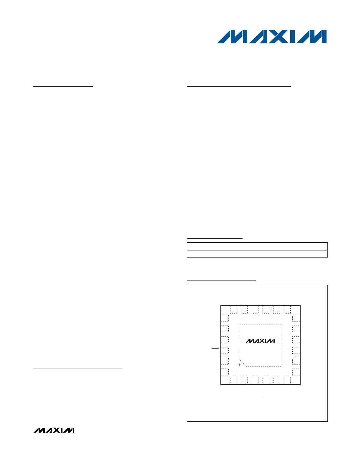
Pin Configuration
Ordering Information
19-4125; Rev 0; 5/08
For pricing, delivery, and ordering information, please contact Maxim Direct at 1-888-629-4642,
or visit Maxim’s website at www.maxim-ic.com.
+
Denotes a lead-free package.
Quick-PWM is a trademark of Maxim Integrated Products, Inc.
PART TEMP RANGE PIN-PACKAGE
MAX17000ETG+ -40°C to +85°C 24 Thin QFN
TOP VIEW
V
PGND1
AGND
SKIP
V
SHDN
19
DD
20
21
22
23
CC
24
1 2
OVP
LX
BST
1718 16 14 13
MAX17000ETG+
PGOOD1
THIN QFN
4mm x 4mm
DH
15
456
3
STDBY
PGOOD2
TONDLCSH
VTTS
VTTR
12
CSL
FB
11
REFIN
10
9
VTTI
VTT
8
PGND2
7
Page 2

MAX17000
Complete DDR2 and DDR3 Memory
Power-Management Solution
2 _______________________________________________________________________________________
ABSOLUTE MAXIMUM RATINGS
ELECTRICAL CHARACTERISTICS
(VIN= 12V, V
CC
= V
DD
= V
SHDN
= V
REFIN
= 5V, V
CSL
= 1.8V, STDBY = SKIP = AGND, TA= 0°C to +85°C, unless otherwise noted.
Typical values are at T
A
= +25°C.) (Note 1)
Stresses beyond those listed under “Absolute Maximum Ratings” may cause permanent damage to the device. These are stress ratings only, and functional
operation of the device at these or any other conditions beyond those indicated in the operational sections of the specifications is not implied. Exposure to
absolute maximum rating conditions for extended periods may affect device reliability.
TON to PGND1 .......................................................-0.3V to +28V
V
DD
to PGND1..........................................................-0.3V to +6V
V
CC
to VDD............................................................-0.3V to +0.3V
OVP to AGND ...........................................................-0.3V to +6V
SHDN, STDBY, SKIP to AGND.................................-0.3V to +6V
REFIN, FB, PGOOD1,
PGOOD2 to AGND ................................-0.3V to (V
CC
+ 0.3V)
CSH, CSL to AGND....................................-0.3V to (V
CC
+ 0.3V)
DL to PGND1..............................................-0.3V to (V
DD
+ 0.3V)
BST to PGND1...........................................................-1V to +34V
BST to LX..................................................................-0.3V to +6V
DH to LX....................................................-0.3V to (V
BST
+ 0.3V)
BST to V
DD
.............................................................-0.3V to +26V
VTTI to PGND2 .........................................................-0.3V to +6V
VTT to PGND2 ............................................-0.3V to (V
TTI
+ 0.3V)
VTTS to AGND............................................-0.3V to (V
CC
+ 0.3V)
VTTR to AGND ..........................................-0.3V to (V
CSL
+ 0.3V)
PGND1, PGND2 to AGND.....................................-0.3V to +0.3V
Continuous Power Dissipation (T
A
= +70°C)
24-Pin, 4mm x 4mm Thin QFN
(derated 27.8mW/°C above +70°C) ..........................2222mW
Operating Temperature Range ...........................-40°C to +85°C
Junction Temperature......................................................+150°C
Storage Temperature Range .............................-65°C to +150°C
Lead Temperature (soldering, 10s) .................................+300°C
PWM CONTROLLER
Input Voltage Range
Output Voltage Range V
Load Regulation Error V
Line Regulation Error VDD = 4.5V to 5.5V, VIN = 4.5V to 26V 0.25 %
Soft-Start Ramp Time t
Soft-Stop Ramp Time t
Soft-Stop Threshold 25 mV
On-Time Accuracy (Note 2) t
PARAMETER SYMBOL CONDITIONS MIN TYP MAX UNITS
V
CC
SSTART
SSTOP
V
IN
, V
CSL
CSL
ON
DD
VIN = 4.5V to 26V,
SKIP = V
CSH
- V
CC
CSL
Rising edge of SHDN 1.4 2.1 ms
Falling edge of SHDN 2.8 ms
V
= 12V,
IN
= 1.2V
V
CSL
326
4.5 5.5
FB = AGND 1.485 1.500 1.515
FB = V
CC
1.782 1.800 1.818Output Voltage Accuracy V
FB = Adj 0.99 1.000 1.01
1 2.7 V
= 0mV to 18mV, SKIP = V
R
= 96.75kΩ
TON
(600kHz), 167ns nominal
R
= 200kΩ (300kHz),
TON
333ns nominal
= 303.25kΩ
R
TON
(200kHz), 500ns nominal
CC
-15 +15
-10 +10
-15 +15
0.1 %
V
V
%
Page 3
MAX17000
Complete DDR2 and DDR3 Memory
Power-Management Solution
_______________________________________________________________________________________ 3
ELECTRICAL CHARACTERISTICS (continued)
(VIN= 12V, V
CC
= V
DD
= V
SHDN
= V
REFIN
= 5V, V
CSL
= 1.8V, STDBY = SKIP = AGND, TA= 0°C to +85°C, unless otherwise noted.
Typical values are at T
A
= +25°C.) (Note 1)
Minimum Off-Time t
Quie scent Supply Current (VDD) I
Quie scent Supply Current (VCC) I
Shutdown Supply C urrent
+ VCC)
(V
DD
TON Pin Shutdown Current I
LINEAR REGULATOR (VTT)
VTTI Input Voltage Range V
VTTI Supply Current I
VTTI Shutdown Current SHDN = AGND, TA = +25°C 10 μA
REFIN Input Bias Current VTTI = 2.8V, REFIN = 1.4V, TA = +25°C -50 +50 nA
REFIN Range V
REFIN Disable Threshold
VTT Internal MOSFET
VTT Output-Accuracy
Source Load
VTT Output-Accuracy
Sink Load
VTT Load Regulation -50μA to -1A I
VTT Line Regulation 1.0V V
VTT Current Lim it
VTT Current-Limit Soft-Start Time With respect to internal VTT_EN signal 160 μs
VTT Discharge MOSFET OVP = VCC 16
VTTS Input Current TA = +25°C 0.1 1.0 μA
PARAMETER SYMBOL CONDITIONS MIN TYP MAX UNITS
OFF(MIN)
I
CC + IDD
TON
VTTI
REFIN
DD
CC
TTI
(Note 2) 250 350 ns
FB forced above 1.0V, STDBY = AGND or
V
= +25°C
CC, TA
FB forced above 1.0V (SMPS, VTT, and
VTTR blocks); STDBY = V
CC
FB forced above 1.0V (ultra-skip and VTTR
blocks); STDBY = AGND
0.01 1.00 μA
2 4 mA
275 475 μA
SHDN = AGND, TA = +25°C 0.01 5 μA
SHDN = AGND, VIN = 26V, VDD = 0 or 5V,
= +25°C
T
A
0.01 1.00 μA
1.0 2.8 V
VTTI = 2.8V, REFIN = 1.4V, no load 10 50 μA
0.5 1.5 V
V
-
High-side on-resistance
(source, I
= 0.1A)
VTT
Low-side on-resistance (sink, I
V
= 1V,
- 5mV) or
(V
REFIN
/2 - 5mV) to
(V
CSL
VTTS, VTT = VTTS
+ 5mV) or
(V
REFIN
/2 + 5mV) to
(V
CSL
VTTS, VTT = VTTS
2.8V, I
TTI
REFIN
= +50μA
I
VTT
V
= 0.5V to 1.5V,
REFIN
= +300mA
I
VTT
V
= 1V,
REFIN
= -50μA
I
VTT
V
= 0.5V to 1.5V,
REFIN
I
= -300mA
VTT
+50μA to +1A 13 17 mV/A
VTT
= ±100mA 1 mV
VTT
CC
0.3
0.12 0.25
= 0.1A) 0.18 0.36
VTT
-5 +5
-5 +5
V
-5
+5
Source 2 4
Sink -4 -2
mV
mV
A
Page 4
MAX17000
Complete DDR2 and DDR3 Memory
Power-Management Solution
4 _______________________________________________________________________________________
ELECTRICAL CHARACTERISTICS (continued)
(VIN= 12V, V
CC
= V
DD
= V
SHDN
= V
REFIN
= 5V, V
CSL
= 1.8V, STDBY = SKIP = AGND, TA= 0°C to +85°C, unless otherwise noted.
Typical values are at T
A
= +25°C.) (Note 1)
REFERENCE BUFFER (VTTR)
VTTR Output Accuracy (Adj) REFIN to VTTR
VTTR Output Accuracy (Preset) V
VTTR Maximum
Recommended Current
FAULT DETECTION (SMPS)
SMPS OVP and PGOOD1
Upper Trip Threshold
SMPS OVP and PGOOD1
Upper Trip Threshold
Fault-Propagation Delay
SMPS Output Undervoltage
Fault-Propagation Delay
SMPS PGOOD1 Lower Trip
Threshold
PGOOD1 Lower Trip Threshold
Propagat ion De la y
PGOOD1 Output Low Voltage I
PGOOD1 Leakage Current I
TON POR Threshold V
FAULT DETECTION (VTT)
PGOOD2 Upper Trip Threshold Hysteresis = 25mV 8 10 13 %
PGOOD2 Lower Trip Threshold Hysteresis = 25mV -13 -10 -8 %
PGOOD2 Propagation Del ay t
PGOOD2 Fault Latch Delay
PGOOD2 Output Low Voltage I
PGOOD2 Leakage Current I
FAULT DETECTION
Thermal-Shutdown Threshold T
VCC Undervoltage Lockout
Threshold
CSL Discharge MOSFET OVP = V
PARAMETER SYMBOL CONDITIONS MIN TYP MAX UNITS
t
OVP
t
UVP
t
PGOOD1
PGOOD1
POR(IN)
PGOOD2
PGOOD2
SHDN
V
UVLO(VCC)
I
= ±1mA -10 +10
VTT
= ±3mA -20 +20
I
VTT
I
= ±1mA -10 +10
/2 to VTTR
CSL
Source/s ink 5 mA
FB forced 25mV above trip threshold 10 μs
Measured at FB, hystere si s = 25mV -12 -15 -18 %
FB forced 50mV below PGOOD1 trip
threshold
= 3mA 0.4 V
SINK
FB = 1V (PGOOD1 high impedance),
PGOOD1 forced to 5V, T
Ri sing edge, PWM disabled below this le vel;
hysteresis = 200mV
VTTS forced 50mV beyond PGOOD2
trip threshold
VTTS forced 50mV beyond PGOOD2
trip threshold
= 3mA 0.4 V
SINK
VTTS = V
PGOOD2 forced to 5V, T
Hysteresis = 15°C160 °C
Rising edge, IC disabled below this le ve l
hysteresis = 200mV
(PGOOD2 high impedance),
REFIN
CC
VTT
= ±3mA -20 +20
I
VTT
12 15 18 %
200 μs
10 μs
= +25°C
A
3.0 V
10 μs
5 ms
= +25°C
A
3.8 4.1 4.4 V
16
mV
1 μA
1 μA
Page 5
MAX17000
Complete DDR2 and DDR3 Memory
Power-Management Solution
_______________________________________________________________________________________ 5
ELECTRICAL CHARACTERISTICS (continued)
(VIN= 12V, V
CC
= V
DD
= V
SHDN
= V
REFIN
= 5V, V
CSL
= 1.8V, STDBY = SKIP = AGND, TA= 0°C to +85°C, unless otherwise noted.
Typical values are at T
A
= +25°C.) (Note 1)
)
)
CURRENT LIMIT
Valley Current-Limit Threshold V
Current-Limit Threshold
(Negative)
Current-Limit Threshold
(Zero Crossing)
SMPS GATE DRIVERS
DH Gate Driver On-Resistance R
DL Gate Driver On-Resistance R
DH Gate Driver Source/
Sink Current
DL Gate Driver Source/
Sink Current
Dead Time t
Internal BST Switch
On-Resistance
LX, BST Leakage Current
INPUTS AND OUTPUTS
Logic Input Threshold
Logic Input Current
Input Leakage Current CSH = 0 or VCC, TA = +25°C -1 +1 μA
Input Bias Current CSL = 0 or V
PARAMETER SYMBOL CONDITIONS MIN TYP MAX UNITS
V
I
DL(SRC
I
DL(SNK
LIMIT
NEG
V
ZX
DH
DL
I
DH
DEAD
R
BST
V
V
V
CSH
CSH
CSH
- V
- V
- V
CSL
, SKIP = V
CSL
CSL
CC
17 20 25 mV
-23 mV
1mV
BST - LX forced to 5V 1.5 5.0 Ω
DL high 1.5 5.0
DL low 0.6 3.0
DH forced to 2.5V, BST - LX forced to 5V 1 A
DL forced to 2.5V 1
DL forced to 2.5V 3
DL rising, TA = +25°C 10 25
DL falling, TA = +25°C 15 35
I
= 10mA,
BST
= 5V internal design target
V
DD
V
BST
T
= +25°C
A
= 26V, SHDN = AGND,
= V
LX
SHDN, STDBY, SKIP, OVP, rising edge
hysteresis = 300mV/600mV (min/max)
SHDN, STDBY, SKIP = 0 or V
= +25°C
T
A
CC
CC
,
1.30 1.65 2.00 V
-1 +1 μA
4.5 Ω
0.001 20 μA
55 100 μA
Ω
A
ns
Page 6
MAX17000
Complete DDR2 and DDR3 Memory
Power-Management Solution
6 _______________________________________________________________________________________
ELECTRICAL CHARACTERISTICS
(VIN= 12V, V
CC
= V
DD
= V
SHDN
= V
REFIN
= 5V, V
CSL
= 1.8V, STDBY = SKIP = AGND, TA= -40°C to +85°C, unless otherwise noted.)
(Note 1)
)
PWM CONTROLLER
Input Voltage Range
On-Time Accuracy (Note 2) t
Minimum Off-Time t
Quiescent Supply Current (VCC)I
LINEAR REGULATOR (VTT)
VTTI Input Voltage Range V
VTTI Supply Current I
REFIN Range V
REFIN Disable Threshold
VTT Internal MOSFET
VTT Load Regulation -50μA to -1A ≤ I
PARAMETER SYMBOL CONDITIONS MIN MAX UNITS
V
IN
, V
V
CC
DD
FB = AGND 1.485 1.520
CSL
VIN = 4.5V to 26V,
SKIP = V
CC
FB = V
CC
FB = Adj 0.990 1.020
R
= 96.75kΩ
TON
(600kHz), 167ns
nominal
R
= 200kΩ
TON
(300kHz), 333ns
nominal
= 303.25kΩ
R
TON
ON
V
V
= 12V,
IN
CSL
= 1.2V
(200kHz), 500ns
nominal
OFF(MIN
(Note 2) 350 ns
FB forced above 1.0V (PWM, VTT, and
CC
VTTR blocks); STDBY = V
FB forced above 1.0V (ultra-skip and
CC
VTTR blocks); STDBY = AGND
VTTI
VTTI
REFIN
VTTI = 2.8V, REFIN = 1.4V, no load 50 μA
H i g h- si d e on- r esi stance ( sour ce, I
Low-side on-resistance (sink, I
≤ +50μA to +1A 17 mV/A
VTT
= 0.1A) 0.25
V T T
= 0.1A) 0.36
VTT
326
4.5 5.5
1.782 1.820Output Voltage Accuracy V
V
V
-15 +15
-10 +10
%
-15 +15
4mA
475 μA
1.0 2.8 V
0.5 1.5 V
V
-
CC
0.3
V
Ω
Page 7
MAX17000
Complete DDR2 and DDR3 Memory
Power-Management Solution
_______________________________________________________________________________________ 7
ELECTRICAL CHARACTERISTICS (continued)
(VIN= 12V, V
CC
= V
DD
= V
SHDN
= V
REFIN
= 5V, V
CSL
= 1.8V, STDBY = SKIP = AGND, TA= -40°C to +85°C, unless otherwise noted.)
(Note 1)
Note 1: Limits are 100% production tested at TA= +25°C. Maximum and minimum limits over temperature are guaranteed by design
and characterization.
Note 2: On-time and off-time specifications are measured from 50% point at the DH pin with LX = GND, V
BST
= 5V, and a 250pF
capacitor connected from DH to LX. Actual in-circuit times might differ due to MOSFET switching speeds.
REFERENCE BUFFER (VTTR)
VTTR Output Accuracy (Adj) REFIN to VTTR
VTTR Output Accuracy (Preset) V
FAULT DETECTION (SMPS)
PGOOD1 Output Low Voltage I
FAULT DETECTION (VTT)
PGOOD2 Output Low Voltage I
FAULT DETECTION
VCC Undervoltage-Lockout
Threshold
CURRENT LIMIT
Valley Current-Limit Threshold V
SMPS GATE DRIVERS
DH Gate Driver On-Resistance R
DL Gate Driver On-Resistance R
Dead Time t
INPUTS AND OUTPUTS
Logic Input Threshold
PARAMETER SYMBOL CONDITIONS MIN MAX UNITS
V
UVLO(VCC)
LIMIT VCSH
DEAD
DH
DL
/2 to VTTR
CSL
=3mA 0.4 V
SINK
=3mA 0.4 V
SINK
Rising edge, IC disabled below this le ve l;
hysteresis = 200mV
- V
CSL
BST - LX forced to 5V 5
DL high 5
DL low 3
DL ris ing 10
DL fal ling 15
SHDN, STDBY, SKIP OVP, rising edge
hysteresis = 300mV/600mV (min/ma x)
I
= ±1mA -10 +10
VTT
= ±3mA -20 +20
I
VTT
I
= ±1mA -10 +10
VTT
= ±3mA -20 +20
I
VTT
4.0 4.4 V
15 25 mV
1.3 2 V
mV
mV
ns
Page 8
MAX17000
Complete DDR2 and DDR3 Memory
Power-Management Solution
8 _______________________________________________________________________________________
Typical Operating Characteristics
(MAX17000 Circuit of Figure 1, V
IN
= 12V, VDD= VCC= 5V, SKIP = GND, TA = +25°C, unless otherwise noted.)
SMPS 1.8V EFFICIENCY
vs. LOAD CURRENT
100
STANDBY MODE
90
80
70
60
SKIP MODE
50
EFFICIENCY (%)
40
30
20
10
0.01 10
LOAD CURRENT (A)
SMPS 1.8V OUTPUT VOLTAGE
vs. LOAD CURRENT
1.82
1.81
1.80
OUTPUT VOLTAGE (V)
1.79
1.78
0.001 10
SKIP MODE
PWM MODE
0.1 10.01
LOAD CURRENT (A)
PWM MODE
10.1
VIN = 7V
VIN = 12V
100
STANDBY MODE
90
MAX17000 toc01
80
70
60
50
EFFICIENCY (%)
40
30
20
10
0.01 10
350
300
MAX17000 toc04
250
200
150
100
SWITCHING FREQUENCY (kHz)
50
0
010
SMPS 1.8V EFFICIENCY
vs. LOAD CURRENT
SKIP MODE
PWM MODE
VIN = 12V
10.1
LOAD CURRENT (A)
SMPS SWITCHING FREQUENCY
vs. LOAD CURRENT
VIN = 12V
V
OUT
4682
LOAD CURRENT (A)
= 1.8V
MAX17000 toc02
EFFICIENCY (%)
10.50
MAX17000 toc05
10.25
10.00
CURRENT LIMIT (A)
SMPS 1.8V EFFICIENCY
vs. LOAD CURRENT
100
STANDBY MODE
90
80
70
60
50
SKIP MODE
40
30
20
10
0.01 10
PWM MODE
VIN = 20V
10.1
LOAD CURRENT (A)
MAX17000 toc03
SMPS VALLEY-CURRENT LIMIT
vs. INPUT VOLTAGE
R
= 2m
Ω
SENSE
MAX17000 toc06
9.75
9.50
428
12 16 20 248
INPUT VOLTAGE (V)
NO-LOAD SUPPLY CURRENT
vs. INPUT VOLTAGE
100
PWM MODE, ICC + I
10
SKIP MODE, ICC + I
1
STANDBY MODE, ICC + I
SUPPLY CURRENT (mA)
0.1
STANDBY MODE, I
0.01
428
DD
PWM MODE, I
DD
SKIP MODE, I
IN
12 16 20 248
INPUT VOLTAGE (V)
NO LOAD
MAX17000 toc07
IN
DD
IN
SAMPLE PERCENTAGE (%)
50
40
30
20
10
0
PRESET 1.5V OUTPUT
VOLTAGE DISTRIBUTION
SAMPLE SIZE = 150 +85°C
1.490 1.510
1.500 1.5051.495
OUTPUT VOLTAGE (V)
+25°C
MAX17000 toc08
Page 9
MAX17000
Complete DDR2 and DDR3 Memory
Power-Management Solution
_______________________________________________________________________________________ 9
Typical Operating Characteristics (continued)
(MAX17000 Circuit of Figure 1, V
IN
= 12V, VDD= VCC= 5V, SKIP = GND, TA = +25°C, unless otherwise noted.)
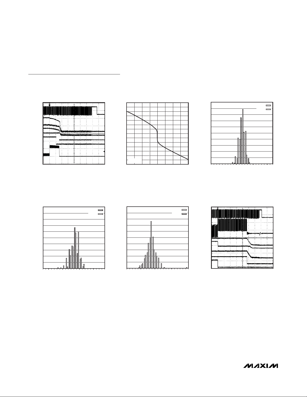
STARTUP WAVEFORM
(HEAVY LOAD)
SHDN
VDDQ
VTT
VTTR
PGOOD1
I
LX
DL
SHDN : 5V/div
VDDQ : 500mV/div
VTT : 500mV/div
VTTR : 500mV/div
200μs/div
PGOOD1 : 2V/div
: 5A/div
I
LX
DL : 5V/div
STANDBY TRANSITION WAVEFORM
STBY
VDDQ
MAX17000 toc09
= 0.25Ω
R
LOAD
SKIP = GND
MAX17000 toc12
VDDQ
VTTR
VTT
PGOOD2
PGOOD1
SHDN
VDDQ
SHUTDOWN WAVEFORM
(DISCHARGE MODE ENABLED)
DL
I
LX
DL : 5V/div
VDDQ : 2V/div
VTT : 1V/div
VTTR : 1V/div
400μs/div
SMPS LOAD-TRANSIENT RESPONSE
(SKIP MODE)
MAX17000 toc10
PGOOD2 : 5V/div
PGOOD1 : 5V/div
SHDN : 10V/div
: 2A/div
I
LX
MAX17000 toc13
STANDBY TRANSITION WAVEFORM
STBY
VDDQ
VTT
TON
DL
LX
I
LX
STBY : 5V/div
VDDQ : 1V/div
VTT : 1V/div
TON: 10V/div
SMPS LOAD-TRANSIENT RESPONSE
VDDQ
2ms/div
(SKIP MODE)
MAX17000 toc11
DL : 5V/div
LX : 10V/div
: 2A/div
I
LX
MAX17000 toc14
VTT
TON
LX
DL
I
LX
STBY : 5V/div
VDDQ : 2V/div
VTT : 1V/div
TON: 10V/div
I
LOAD
LX
I
LX
VDDQ : 50mV/div
LX : 10V/div
20μs/div
I
LOAD
I
LX
: 5A/div
: 5A/div
200μs/div
LX : 10V/div
: 10A/div
I
LX
DL : 5V/div
I
LOAD
LX
I
LX
VDDQ : 50mV/div
LX : 10V/div
20μs/div
I
LOAD
I
LX
: 5A/div
: 5A/div
Page 10
MAX17000
Complete DDR2 and DDR3 Memory
Power-Management Solution
10 ______________________________________________________________________________________
Typical Operating Characteristics (continued)
(MAX17000 Circuit of Figure 1, V
IN
= 12V, VDD= VCC= 5V, SKIP = GND, TA = +25°C, unless otherwise noted.)
OUTPUT OVERLOAD WAVEFORM
DL
VDDQ
VTT
VTTR
PGOOD2
PGOOD1
I
LX
DL : 5V/div
VDDQ : 1V/div
VTT : 1V/div
VTTR : 1V/div
400μs/div
VTT SOURCE CURRENT LIMIT
50
SAMPLE SIZE = 150 +85°C
40
30
20
SAMPLE PERCENTAGE (%)
10
0
2.0 4.0
3.0 3.52.5
CURRENT LIMIT (A)
MAX17000 toc15
PGOOD2 : 2V/div
PGOOD1 : 2V/div
: 10A/div
I
LX
+25°C
0.79
0.78
0.77
0.76
0.75
VTT VOLTAGE (V)
0.74
0.73
0.72
-2.0 2.0
50
40
MAX17000 toc18
30
20
SAMPLE PERCENTAGE (%)
10
0
-4.0 -2.0
vs. SOURCE/SINK LOAD CURRENT
VTT VOLTAGE
V
= 18V
TTI
-0.5 0 0.5 1.51.0-1.5 -1.0
LOAD CURRENT (A)
VTT SINK CURRENT LIMIT
SAMPLE SIZE = 150 +85°C
-3.0 -2.5-3.5
CURRENT LIMIT (A)
+25°C
50
40
MAX17000 toc16
30
20
SAMPLE PERCENTAGE (%)
10
0
-15.0 -5.0
DL
MAX17000 toc19
I
LX
VDDQ
VTT
VTTR
PGOOD1
PGOOD2
VTT OFFSET VOLTAGE DISTRIBUTION
AT 300mA LOAD
SAMPLE SIZE = 150 +85°C
-10.0 -7.5-12.5
OFFSET VOLTAGE (mV)
+25°C
VTT OVERLOAD FAULT WAVEFORMS
DL : 5V/div
: 2A/div
I
LX
VDDQ : 2V/div
VTT : 1V/div
(5ms TIMER)
1ms/div
MAX17000 toc20
VTTR : 1V/div
PGOOD1 : 2V/div
PGOOD2 : 2V/div
MAX17000 toc17
Page 11

MAX17000
Complete DDR2 and DDR3 Memory
Power-Management Solution
______________________________________________________________________________________ 11
Typical Operating Characteristics (continued)
(MAX17000 Circuit of Figure 1, V
IN
= 12V, VDD= VCC= 5V, SKIP = GND, TA = +25°C, unless otherwise noted.)
VTT LOAD-TRANSIENT RESPONSE (SOURCE)
BETWEEN 10mA AND 1.5A
I
VTT
I
VTT
VTT_ac
VDDQ = 1.8V
I
: 1A/div
VTT
VTT : 20mV/div
VTT LOAD-TRANSIENT RESPONSE
(SOURCE-SINK)
I
VTT
VTT_ac
I
: 1A/div
VTT
VTT : 20mV/div
20μs/div
20μs/div
MAX17000 toc21
MAX17000 toc23
VDDQ = 1.8V
VTT LOAD-TRANSIENT RESPONSE
I
VTT
VTT_ac
VDDQ = 1.8V
I
: 1A/div
VTT
VTT : 20mV/div
0.79
0.78
0.77
0.76
0.75
0.74
0.73
OUTPUT VOLTAGE (V)
0.72
0.71
0.70
-6 6
(SINK)
20μs/div
VTTR OUTPUT VOLTAGE
vs. LOAD CURRENT
-2 0 2 4-4
LOAD CURRENT (A)
MAX17000 toc22
MAX17000 toc24
Page 12

MAX17000
Complete DDR2 and DDR3 Memory
Power-Management Solution
12 ______________________________________________________________________________________
Pin Description
PIN NAME FUNCTION
OVP Mode Control. This input selectively enables/disables the SMPS OV protection feature and
output discharge mode. When enabled, the SMPS OV protection feature is enabled. Connect OVP to
1 OVP
2 PGOOD1
3 PGOOD2
4 STDBY
5 VTTS
6 VTTR
7 PGND2 Power Ground for VTT. Connect PGND2 externally to the underside of the exposed pad.
8 VTT
9 VTTI
10 REFIN
11 FB
12 CSL
13 CSH
the following voltage levels for the desired function:
High (> 2.4V) = Enable SMPS OV protection, and SMPS and VTT discharge FETs.
Low (GND) = Disable SMPS OV protection, and SMPS and VTT discharge FETs.
Open-Drain Power-Good Output. PGOOD1 is low when the SMPS output voltage is more than 15%
(typ) beyond the normal regulation point, during soft-start, and in shutdown.
After the soft-start circuit has terminated, PGOOD1 becomes high impedance if the SMPS output is in
regulation.
Open-Drain Power-Good Output. PGOOD2 is low when the VTT output voltage is more than 10% (typ)
beyond the normal regulation point, in shutdown, and in standby.
After the SMPS soft-start circuit has terminated, PGOOD2 becomes high impedance if the VTT output
is in regulation.
Standby Control Input. When SHDN is high and STDBY is low, the MAX17000 enters a low-quiescent
current mode, putting the SMPS in ultra-skip operation and turning off the VTT output (high-Z). This
mode helps save converter power loss in computer standby operation.
When STDBY is high, normal SMPS operation resumes and the VTT output is enabled.
Sense Pin for Termination Supply Output. Normally connected to the VTT pin to allow accurate
regulation to V
Termination Reference Buffer Output. VTTR tracks V
tracks V
REFIN
0.33μF ceramic capacitor.
Termination Power-Supply Output. Connect VTT to VTTS to regulate the VTT voltage to the VTTS
regulation setting.
Termination Power-Supply Input. VTTI is the input power supply to the VTT linear regulator. Normally
connected to the output of the SMPS regulator for DDR applications.
External Reference Input. REFIN sets the feedback regulation voltage (VTTR = VTTS = V
MAX17000.
Connect REFIN to V
Connect a 0.5V to 1.5V voltage input to set the adjustable output for VTT, VTTS, and VTTR.
Feedback Input for SMPS Output. Connect to V
+1.5V output. For an adjustable output (1.0V to 2.7V), connect FB to a resistive divider from the output
voltage. FB regulates to +1.0V.
Negative Input of the PWM Output Current-Sense and Supply Input for VTTR. Connect CSL to the
negative side of the output current-sensing resistor or the filtering capacitor if the DC resistance of the
output inductor is utilized for current sensing.
C S L i s al so the p ath for the i nter nal 16_ d i schar g e M OS FE T w hen V
Positive Input of the PWM Output Current Sense. Connect CSH to the positive side of the output
current-sensing resistor or the filtering capacitor if the DC resistance of the output inductor is utilized
for current sensing.
/2 or the REFIN voltage.
CSL
when a voltage between 0.5V to 1.5V is set at REFIN. Decouple VTTR to AGND with a
to use the internal V
CC
CSL
CSL
/2 divider.
for a fixed +1.8V output or to AGND for a fixed
CC
/2 when REFIN is connected to VCC. VTTR
) of the
REFIN
U V LO occur s w i th OV P enab l ed .
C C
Page 13

MAX17000
Complete DDR2 and DDR3 Memory
Power-Management Solution
______________________________________________________________________________________ 13
Pin Description (continued)
PIN NAME FUNCTION
Switching Frequency Setting Input. An external resistor between the input power source and th is
pin sets the switching frequency per phase according to the following equation:
= C
T
14 TON
15 DH High-Side Gate-Driver Output. Swings from LX to BST. DH is low when in shu tdown or UVLO.
16 LX Inductor Connection. Connect LX to the switched side of the inductor as shown in Figure 1.
17 BST
18 DL Synchronous-Rectifier Gate-Driver Output. DL swings from VDD to PGND1.
19 V
20 PGND1 Power Ground. Ground connect ion for the low-side MOSFET gate driver.
21 AGND Analog Ground. Connect backside exposed pad to AGND.
22 SKIP
23 V
24 SHDN
— EP Exposed Pad. Connect backside exposed pad to AGND.
DD
CC
SW
where C
TON is high impedance in shutdown.
Boost Flying Capacitor Connection. Connect to an external 0.1μF, 6V capacitor as shown in Figure
1. The MAX17000 contains an internal boost switch.
Supply Voltage Input for the DL Gate Dri ver and 3.3V Reference/Analog Supply. Connect to the
system supply voltage (+4.5V to +5.5V). Bypass V
ceramic capacitor.
Pulse-skipping Control Input. This input determines the mode of operation under normal steadystate condit ion s and dynamic output voltage transitions:
High (> 2.4V) = Forced-PWM operation
Low (AGND) = Pulse-skipping mode
Controller Supply Voltage. Connect to a 4.5V to 5.5V source. Bypas s VCC to AGND with a 1μF or
greater ceramic capacitor.
Shutdown Control Input. Connect to V
MAX17000 s lowly ramps down the output voltage to ground. When the internal target voltage
reaches 25mV, the controller forces DL low, and enters the low current (1μA) shutdown state.
When discharge mode is enabled by OVP (OVP = high), the CSL and VTT internal 16 discharge
MOSFETs are enab led in shutdown. When d ischarge mode is disabled b y OVP (OVP = low), LX,
VTT, and VTTR are high impedance in shutdown.
A rising edge on SHDN clears the fault OV protection latch.
x (R
TON
= 16.26pF.
TON
+ 6.5k)
TON
to power ground with a 1μF or greater
DD
for normal operation. When SHDN is pulled low, the
CC
Page 14

MAX17000
Standard Application Circuits
The MAX17000 standard application circuit (Figure 1)
generates the VDDQ, VTT, and VTTR rails for DDR,
DDR2, or DDR3 in a notebook computer. See Table 1 for
component selections. Table 2 lists the component manufacturers. Table 3 is the operating mode truth table.
Complete DDR2 and DDR3 Memory
Power-Management Solution
14 ______________________________________________________________________________________
Table 1. Component Selection for Standard Applications
Table 2. Component Suppliers
COMPONENT
Input Capacitor
Output Capacitor
Inductor
Current-Sensing Resistor
MOSFETs
INDUCTORS
Dale (Vishay) 402-563-6866 (USA) www.vishay,com
NEC/TOKIN America, Inc. 510-324-4110 (USA) www.nec-tokinamerica.com
Panasonic Corp. 65-231-3226 (Singapore), 408-749-9714 (USA) www.panasonic.com
Sumida Corp. 408-982-9660 (USA) www.sumida.com
TOKO America, Inc. 858-675-8013 (USA) www.tokoam.com
CAPACITORS
AVX Corp. 843-448-9411 (USA) www.avxcorp.com
KEMET Corp. 408-986-0424 (USA) www.kemet.com
Panasonic Corp. 65-231-3226 (Singapore), 408-749-9714 (USA) www.panasonic.com
SANYO Electric Co., Ltd. 81-72-870-6310 (Japan), 619-661-6835 (USA) www.sanyodevice.com
Taiyo Yuden 03-3667-3408 (Japan), 408-573-4150 (USA) www.t-yuden.com
TDK Corp. 847-803-6100 (USA), 81-3-5201-7241 (Japan) www.component.tdk.com
SENSING RESISTORS
Vishay 402-563-6866 (USA) www.vishay,com
MOSFET
Fairchild Semiconductor 800-341-0392 (USA) www.fairchildsemi.com
DIODES
Central Semiconductor Corp. 631-435-1110 www.centralsemi.com
Nihon Inter Electronics Corp. 81-3-3343-84-3411 (Japan) www.niec.co.jp
SUPPLIER PHONE WEBSITE
(2x) 10μF, 25V
Taiyo Yuden TMK432BJ106KM
(2x) 330μF, 2.5V ,12mΩ (C2 case)
SANYO 2R5TPE330MCC2
1.4μH, 12A, 3.4mΩ (typ)
Sumida CDEP105(L)NP-1R4
2mΩ, 0.5W (2010)
Vishay WSL20102L000FEA
30V, 20A n-channel MOSFET (high side)
Fairchild FDMS8690;
30V, 40A n-channel MOSFET (low side)
Fairchild FDMS8660S
V
= 1.5V TO 1.8V AT 10A V
OUT
= 7V TO 20V (300kHz) VIN = 7V TO 16V (500kHz)
V
IN
= 1.5V TO 1.8V AT 6A
OUT
10μF, 25V
Taiyo Yuden TMK432BJ106KM
(2x) 220μF, 2.5V, 21mΩ (B2 case)
SANYO 2R5TPE220MLB
1.4μH, 12A, 3.4mΩ (typ)
Sumida CDEP105(L)NP-1R4
3mΩ, 0.5W (2010)
Vishay WSL20103L000FEA
30V 20A n-channel MOSFET (high side)
Fairchild FDMS8690;
30V 40A n-channel MOSFET (low side)
Fairchild FDMS8660S
Page 15

MAX17000
Complete DDR2 and DDR3 Memory
Power-Management Solution
______________________________________________________________________________________ 15
Table 3. Operating Mode Truth Table
SHDN STDBY SKIP OPERATION
SMPS output ramps up in skip mode with a 1.4ms (typ) ramp time. PGOOD1 is held low until the
1L → HL → HX
2L → HL X
3HL → HX
4H H H
5H H L
6H L X
7H → LH X
8H → LL X
9L X X
SMPS output is in regulation.
VTT and VTTR ramp up to the final voltage based on V
VTT is in regulation.
SMPS output ramps up in skip mode with a 1.4ms ramp time. PGOOD1 is held low until the SMPS
output is in regulation.
O nce C S L or FB i s i n r eg ul ati on, the P W M b l ock tur ns off and enter s stand b y m od e.
VTT remains off throughout since STDBY is low. PGOOD2 stays low throughout. The VTT discharge
FET is enabled if OVP is high, but disabled if OVP is low.
VTTR ramps up to the final voltage based on V
Ultra-skip and standby modes are exited and the full current capability of the MAX17000 is
available.
VTT ramps up after the internal SMPS block is ready. VTT ramps to the final voltage based on
V
/2 or V
CSL
PGOOD2 goes high when VTT is in regulation.
SMPS output is in forced-PWM mode.
VTT and VTTR are enabled.
PGOOD1 is high when the SMPS output is in regulation.
PGOOD2 is high when VTT is in regulation.
SMPS output is in normal skip mode.
VTT and VTTR are enabled.
PGOOD1 is high when the SMPS output is in regulation.
PGOOD2 is high when VTT is in regulation.
SMPS output is in ultra-skip mode.
VTT is off and is high impedance.
PGOOD2 is forced low.
VTTR is active and regulates to V
U l tr a- ski p or ski p m od e i s exi ted as the M AX 17000 r am p s the outp ut d ow n to zer o.
V TTR tr acks V
Ultra-skip or skip mode is exited as the MAX17000 ramps the output down to zero.
VTTR tracks V
low. VTT is not enabled throughout soft-shutdown.
DL low. Internal16Ω discharge MOSFETs on CSL and VTT enabled if OVP is high, but disabled if
OVP is low.
REFIN
C S L
CSL
.
/2 or V
/2 or V
/2 or V
CSL
/2 or V
CSL
/2 or V
CSL
d ur i ng shutd ow n. After the S M P S outp ut r eaches 25m V , D L g oes l ow .
R E F IN
during shutdown. After the SMPS output reaches 25mV, DL goes
REFIN
REFIN
REFIN
.
. PGOOD2 is held low until
REFIN
.
Page 16

MAX17000
Complete DDR2 and DDR3 Memory
Power-Management Solution
16 ______________________________________________________________________________________
Detailed Description
The MAX17000 complete DDR solution comprises a
step-down controller, a source-sink LDO regulator, and a
reference buffer. Maxim’s proprietary Quick-PWM pulsewidth modulator in the MAX17000 is specifically
designed for handling fast load steps while maintaining a
relatively constant operating frequency and inductor
operating point over a wide range of input voltages. The
Quick-PWM architecture circumvents the poor load-transient timing problems of fixed-frequency current-mode
PWMs, while also avoiding the problems caused by
widely varying switching frequencies in conventional constant-on-time and constant-off-time PWM schemes.
Figure 1 is the MAX17000 standard application circuit
and Figure 2 is the MAX17000 functional diagram.
The MAX17000 includes a ±2A source-sink LDO regulator for the memory termination rail. The source-sink
regulator features a dead band that either sources or
sinks, ideal for the fast-changing short-period loads
presenting in memory termination applications. This
feature also reduces the VTT output capacitance
requirement down to 1μF, though load-transient
response can still require higher capacitance values
between 10μF and 20μF.
The reference buffer sources and sinks ±3mA, generating
a reference rail for use in the memory controller and
memory devices.
Figure 1. MAX17000 Standard Application Circuit
R
TON
+5V
100kΩR2100kΩ
5V V
+5V
C
VDD
1μF
PGND
CC
1
OVP
R3
2
PGOOD1
3
PGOOD2
19
V
DD
R1
10Ω
23
V
C
VCC
1μF
AGND
SLP_S3#
ON/OFF
V
CC
CC
21
4
24
22
10
AGND
STDBY
SHDN
SKIP
REFIN
AGND
MAX17000
EP
TON
BST
PGND1
CSH
CSL
VTTI
PGND2
VTT
VTTS
VTTR
PGND
DH
14
17
15
C
BST
0.1μF
16
LX
18
DL
20
13
12
11
FB
9
7
PGND
8
5
6
N
L
R
FBA
R
FBB
AGND
C
VTTR
0.33μF
AGND
N
H
PGND
FB OPTIONS:
1. CONNECT FB TO 5V FOR FIXED +1.8V.
2. CONNECT FB TO GND FOR FIXED +1.5V.
3. USE FB RESISTOR-DIVIDER FOR ADJUSTABLE
OUTPUT VOLTAGES.
C
C
V
7V TO 20V
D1
VTTI
VTT
IN
C
PGND
L1
+1V TO + 2.5V
VTT = VDDQ/2
VTTR = VDDQ/2
IN
R
SENSE
VDDQ
+1.8V OR 1.5V
C
OUT
PGND
Page 17

MAX17000
Complete DDR2 and DDR3 Memory
Power-Management Solution
______________________________________________________________________________________ 17
TON
Figure 2. MAX17000 Functional Diagram
STDBY
OVP
PGOOD1
CSL
SMPS
RUN
SMPS FAULT
DETECTION
OVF
VTT
FAULT
RUN
POWER-GOOD1
RUN
ERROR
AMP
ON-TIME
COMPUTE
1.2V
10ms
TIMER
OVF
VTT FAULT
UVF
SMPS
FAULT
SMPS
FAULT
LATCH
TON
TRIG Q
1-SHOT
STDBY EA
INT_FB
0.7V
1.15V
MAX17000
t
OFF(MIN)
TRIGQ
1-SHOT
SRQ
S
Q
R
ZERO CROSSING
VALLEY CURRENT LIMIT
EA
RUN
SMPS RUN
SOFT-START/STOP
1V REF
INT_FB
3mV
20mV
DECODE
INT_REF
BST
DH
LX
VDD
DL
PGND1
STDBY
SKIP
CSL
CSH
SHDN
FB
FB
VCC
PGOOD2
REFIN
POWER-GOOD2
VDD - 0.3V
CSL
1.4ms
SMPS
FAULT
R
R
RUN
OVP
VTT WINDOW
COMPARATOR
5ms
TIMER
SMPS RUNOK
STDBY
V
CC
UVLO
VTT
FAULT
VTTI
VTT
VTT SS
CURRENT LIMIT
VTT
PGND2
PGND2
CURRENT LIMIT
CURRENT LIMIT
VTT
16Ω
VTT POS
VTT NEG
VTT_EN
16Ω
CSL
PGND1
5mV
5mV
VTT_EN
V
DD
V
DD
PGND2
CSL
AGND
VTTS
VTTI
VTT
PGND2
VTTR
Page 18

MAX17000
Complete DDR2 and DDR3 Memory
Power-Management Solution
18 ______________________________________________________________________________________
+5V Bias Supply (VDD, VCC)
The MAX17000 requires an external 5V bias supply in
addition to the battery. Typically, this 5V bias supply is
the notebook’s 95% efficient 5V system supply.
Keeping the bias supply external to the IC improves
efficiency and eliminates the cost associated with the
5V linear regulator that would otherwise be needed to
supply the PWM circuit and gate drivers. If stand-alone
capability is needed, the 5V supply can be generated
with an external linear regulator such as the MAX1615.
The 5V bias supply powers both the PWM controller
and internal gate-drive power, so the maximum current
drawn is:
I
BIAS
= IQ+ fSWQ
G(MOSFETs)
= 2mA to 20mA (typ)
where I
Q
is the current for the PWM control circuit, f
SW
is the switching frequency, and Q
G(MOSFETs)
is the
total gate-charge specification limits at VGS= 5V for the
internal MOSFETs.
Free-Running Constant-On-Time PWM
Controller with Input Feed-Forward
The Quick-PWM control architecture is a pseudo-fixedfrequency, constant on-time, current-mode regulator
with voltage feed-forward. This architecture utilizes the
output filter capacitor’s ESR to act as a current-sense
resistor, so the output ripple voltage can provide the
PWM ramp signal. In addition to the general QuickPWM, the MAX17000 also senses the inductor current
through DCR method or with a sensing resistor.
Therefore, it is less dependent on the output capacitor
ESR for stability. The control algorithm is simple: the
high-side switch on-time is determined solely by a oneshot whose pulse width is inversely proportional to input
voltage and directly proportional to output voltage.
Another one-shot sets a minimum off-time (250ns typ).
The on-time one-shot is triggered if the error comparator is low, the low-side switch current is below the valley
current-limit threshold, and the minimum off-time oneshot has timed out.
On-Time One-Shot
The heart of the PWM core is the one-shot that sets the
high-side switch on-time. This fast, low-jitter, adjustable
one-shot includes circuitry that varies the on-time in
response to battery and output voltages. The high-side
switch on-time is inversely proportional to the battery
voltage as measured by the VINinput, and proportional
to the output voltage.
An external resistor between the input power source
and TON pin sets the switching frequency per phase
according to the following equation:
where C
TON
= 16.26pF, and 0.075V is an approximation to accommodate for the expected drop across the
low-side MOSFET switch. This algorithm results in a
nearly constant switching frequency despite the lack of
a fixed-frequency clock generator.
For loads above the critical conduction point, where the
dead-time effect is no longer a factor, the actual switching frequency is:
where V
DIS
is the sum of the parasitic voltage drops in
the inductor discharge path, including synchronous
rectifier, inductor, and PCB resistances; V
CHG
is the
sum of the parasitic voltage drops in the charging path,
including the high-side switch, inductor, and PCB resistances; and tONis the on-time calculated by the
MAX17000.
Automatic Pulse-Skipping Mode
(
SKIP
= AGND)
In skip mode (SKIP = AGND), an inherent automatic
switchover to PFM takes place at light loads. This
switchover is affected by a comparator that truncates
the low-side switch on-time at the inductor current’s
zero crossing.
DC output-accuracy specifications refer to the threshold of the error comparator. When the inductor is in
continuous conduction, the MAX17000 regulates the
valley of the output ripple, so the actual DC output voltage is higher than the trip level by 50% of the output
ripple voltage. In discontinuous conduction (SKIP =
AGND and I
OUT
< I
LOAD(SKIP)
), the output voltage has
a DC regulation level higher than the error-comparator
threshold by approximately 1.5% due to slope compensation. However, the internal integrator corrects for
most of it, resulting in very little load regulation.
STDBY = AGND overrides the SKIP pin setting, forcing
the MAX17000 into standby.
CR kV V
×+×+(.)(.)65 0075Ω
t
ON
TON TON CSL
=
f
=
SW
CR k
TON TON
f
=
SW
tVVV
ON IN CHG DIS
V
IN
1
×+
VV
OUT DIS
×− +()
65(.)Ω
+
Page 19

MAX17000
Complete DDR2 and DDR3 Memory
Power-Management Solution
______________________________________________________________________________________ 19
The MAX17000 always uses skip mode during startup,
regardless of the SKIP and STDBY setting. The SKIP
and STDBY controls take effect after soft-start is done.
See Figure 3.
Forced-PWM Mode (
SKIP
= VCC)
The low-noise forced-PWM mode (SKIP = VCC) disables
the zero-crossing comparator, which controls the lowside switch on-time. This forces the low-side gate-drive
waveform to constantly be the complement of the highside gate-drive waveform, so the inductor current
reverses at light loads while DH maintains a duty factor
of V
OUT/VIN
. The benefit of forced-PWM mode is to keep
a fairly constant switching frequency. However, forcedPWM operation comes at a cost: the no-load 5V bias
current remains between 2mA to 20mA, depending on
the switching frequency.
STDBY = AGND overrides the SKIP pin setting, forcing
the MAX17000 into standby.
The MAX17000 switches to forced-PWM mode during
shutdown, regardless of the state of SKIP and STDBY
levels.
Standby Mode (
STDBY
)
It should be noted that standby mode in the MAX17000
corresponds to computer system standby operation,
and is not referring to the MAX17000 shutdown status.
When standby mode is enabled (STDBY = AGND), the
MAX17000 switches over from the fast internal PWM
block to a low-quiescent current mode using a lowpower valley comparator to initiate an on-time pulse.
The zero-crossing comparator is enabled so that the
MAX17000 only operates in discontinuous mode,
reducing the maximum available output current by 1/6.
The system is NOT expected to have any fast load transients in such a state. While in standby, VTT is disabled
(high impedance) but VTTR remains active. SKIP is
ignored when standby mode is enabled.
When standby mode is disabled (STDBY = VCC), the
MAX17000 reenables its fast internal PWM block. Once
the internal SMPS block is ready, the VTT block is
enabled and the VTT output capacitor is charged. The
VTT soft-start current limit increases linearly from zero
to its maximum current limit in 160μs (typ), keeping the
input VTTI inrush low. See Figure 4.
Figure 3. Pulse-Skipping/Discontinuous Crossover Point
Figure 4. MAX17000 Standby Mode Timing
ΔI
V
- V
IN
OUT
=
Δt
INDUCTOR CURRENT
L
ON-TIME0 TIME
I
LOAD
I
PEAK
= I
/2
PEAK
STDBY
SMPS_RUNOK
SMPS OUTPUT
VTTR OUTPUT
VTT OUTPUT
VTT CURRENT LIMIT
PGOOD1
PGOOD2
< 50μs
VTT HIGH IMPEDANCE
160μs
Page 20

MAX17000
Complete DDR2 and DDR3 Memory
Power-Management Solution
20 ______________________________________________________________________________________
Valley Current-Limit Protection
The MAX17000 uses the same valley current-limit protection employed on all Maxim Quick-PWM controllers. If
the current exceeds the valley current-limit threshold,
the PWM controller is not allowed to initiate a new cycle.
The actual peak current is greater than the valley current-limit threshold by an amount equal to the inductor
ripple current. Therefore, the exact current-limit characteristic and maximum load capability are a function of
the inductor value and battery voltage. When combined
with the undervoltage-protection circuit, this current-limit
method is effective in almost every circumstance.
In forced-PWM mode, the MAX17000 also implements
a negative current limit to prevent excessive reverse
inductor currents when V
OUT
is sinking current. The
negative current-limit threshold is set to approximately
115% of the positive current limit. See Figure 5.
Power-Good Outputs
(PGOOD1 and PGOOD2)
The MAX17000 features two power-good outputs.
PGOOD1 is the open-drain output for a window comparator that continuously monitors the SMPS output.
PGOOD1 is actively held low in shutdown and during
soft-start and soft-shutdown. After the soft-start terminates, PGOOD1 becomes high impedance as long as
the SMPS output voltage is between 115% (typ) and
85% (typ) of the regulation voltage. When the SMPS
output voltage exceeds the 115%/85% regulation window, the MAX17000 pulls PGOOD1 low. Any fault condition on the SMPS output forces PGOOD1 and
PGOOD2 low and latches off until the fault latch is
cleared by toggling SHDN or cycling VCCpower below
1V. Detection of an OVP event immediately pulls
PGOOD1 low, regardless of the OVP state (OVP
enabled or disabled).
PGOOD2 is the open-drain output for a window comparator that continuously monitors the VTT output.
PGOOD2 is actively held low in standby, shutdown,
and during soft-start. PGOOD2 becomes high impedance as long as the VTT output voltage is within ±10%
of the regulation voltage. When the VTT output exceeds
the ±10% threshold, the MAX17000 pulls PGOOD2 low.
If PGOOD2 remains low for 5ms (typ), the MAX17000
latches off with the soft-shutdown sequence.
For logic-level output voltages, connect an external 100kΩ
pullup resistor from PGOOD1 and PGOOD2 to VDD.
POR, UVLO
Power-on reset (POR) occurs when VCCrises above
approximately 2V, resetting the fault latch and soft-start
circuit and preparing the controller for power-up. When
OVP protection is enabled, a rising edge on POR turns
on the 16Ω discharge MOSFET on CSL and VTT. When
OVP is disabled, the internal 16Ω discharge MOSFETs
on CSL and VTT also remain off.
VCCundervoltage lockout (UVLO) circuitry inhibits
switching until VCCreaches 4.1V (typ). When VCCrises
above 4.1V, the controller activates the PWM controller
and initializes soft-start. When VCCdrops below the
UVLO threshold (falling edge), the controller stops, DL
is pulled low, and the internal 16Ω discharge
MOSFETs on the CSL and VTT outputs are enabled, if
OVP is enabled.
Soft-Start and Soft-Shutdown
Soft-start and soft-shutdown for the MAX17000 PWM
block is voltage based. Soft-start begins when SHDN is
driven high. During soft-start, the PWM output is
ramped up from 0V to the final set voltage in 1.4ms.
This reduces inrush current and provides a predictable
ramp-up time for power sequencing. The MAX17000
always uses skip mode during startup, regardless of
the SKIP and STDBY setting. The SKIP and STDBY con-
trols take effect after soft-start is done.
The MAX17000 VTT LDO regulator uses a current-limited
soft-start function. When the VTT block is enabled, the
internal source and sink current limits are linearly
increased from zero to the full-scale limit in 160μs. Fullscale current limit is available when the VTT output is in
regulation, or after 160μs, whichever is earlier. The VTTR
reference buffer does not have any soft-start control.
Figure 5. Valley Current-Limit Threshold Point
I
PEAK
I
LOAD
I
LIMIT
I
= I
LIM(VAL)
INDUCTOR CURRENT
0 TIME
LOAD(MAX)
LIR
1-
()
2
Page 21

MAX17000
Complete DDR2 and DDR3 Memory
Power-Management Solution
______________________________________________________________________________________ 21
Soft-shutdown begins after SHDN goes low, an output
undervoltage fault occurs, or a thermal fault occurs. A
fault on the SMPS (UV fault for more than 200μs (typ)),
or fault on the VTT output that persists for more than
5ms (typ), triggers shutdown of the whole IC. During
soft-shutdown, the output is ramped down to 0V in
2.8ms, reducing negative inductor currents that can
cause negative voltages on the output. At the end of
soft-shutdown, DL is driven low.
When OVP is enabled (OVP = V
CC
), the internal 16Ω
discharging MOSFETs on CSL and VTT are enabled
until startup is triggered again by a rising edge of
SHDN. When OVP is disabled (OVP = AGND), the CSL
and VTT internal 16Ω discharging MOSFETs are not
enabled in shutdown.
Output Fault Protection
The MAX17000 provides overvoltage/undervoltage fault
protections for the PWM output. Drive OVP to enable
and disable fault protection as shown in Table 4.
SHDN
Figure 6. MAX17000 Startup/Shutdown Timing when OVP Is Enabled
STDBY
INT_REF
REFOK
SMPS_RUNOK
1.4ms
SMPS OUTPUT
VTT OUTPUT
VTTR OUTPUT
VTT CURRENT LIMIT
PGOOD1
PGOOD2
DL
VTT 16Ω FET
CSL 16Ω FET
160μs
SKIP FPWM
2.8ms
25mV
Page 22

MAX17000
Complete DDR2 and DDR3 Memory
Power-Management Solution
22 ______________________________________________________________________________________
Table 4. Fault Protection and Shutdown Setting Truth Table
OVP Disabl ed
Discharge Disabled
(OVP = Low)
OVP Enabled
Discharge Enabled
(OVP = H igh)
OVP Enabled
Discharge Enabled
(OVP = H igh)
OVP MODE REACTION/DRIVER STATE COMMENT
DL immediately pulled low.
Shutdown
(SHDN = low)
SMPS UVP
SMPS OVP
(disabled)
VTT < -90% or
VTT > +110%
V
UVLO
CC
falling edge
Shutdown
(SHDN = low)
SMPS UVP
SMPS OVP
(enabled)
VTT < 90% or
VTT > 110%
UVLO
V
CC
falling edge
VTTR trac ks the SMPS output during soft-shutdown. CSL and VTT
are high impedance at the end of soft-shutdown (16 discharge
MOSFETs disabled).
DL immediately pulled low.
VTTR trac ks the SMPS output during soft-shutdown. CSL and VTT
are high impedance at the end of soft-shutdown (16 discharge
MOSFETs disabled).
Controller remains acti ve (normal operation).
Note: An OVP detection still pulls PGOOD1 low.
PGOOD2 immediately pulled low.
Soft-shutdown init iated if fault persists for more than 5ms (typ). DH
not used in soft-shutdown. DL low after soft-shutdown completed.
VTTR tracks the SMPS output soft-shutdown.
DL and DH immediately pu lled low.
PGOOD1 and PGOOD2 immediatel y forced low. VTT and VTTR
blocks immed iately disabled (high impedance, no 16 discharge
on output s).
Soft-shutdown initiated.
DL high after soft-shutdown completed.
VTTR tracks the SMPS output during soft-shutdown. Internal 16
discharge MOSFETs on CSL and VTT enabled after soft-shutdown.
Soft-shutdown initiated. DH not used in soft- shutdown. DL low
after soft-shutdown completed.
VTTR tracks the SMPS output dur ing soft-shutdown. Internal 16
discharge MOSFETs on CSL and VTT enabled after soft-shutdown.
DL immediate ly latched high, DH forced low.
PGOOD1 and PGOOD2 immediatel y forced low.
VTT and VTTR blocks immediately shut down. Internal 16
discharge MOSFETs on CSL and VTT enab led.
PGOOD2 immediately pulled low.
Soft-shutdown init iated if fault persists for more than 5ms (typ). DH
not used in soft-shutdown. DL low after soft-shutdown completed.
VTTR tracks the SMPS output during soft-shutdown. Internal 16
discharge MOSFETs on CSL and VTT enabled after soft-shutdown.
DL and DH immediately pu lled low.
PGOOD1 and PGOOD2 immediatel y forced low.
VTT and VTTR blocks immediately disabled.
Internal 16 discharge MOSFETs on CSL and VTT enabled
immediately.
Outputs high-
impedance in
shutdown.
SMPS latched fault
condition.
Only PGOOD1 pulled
low; fault not latched.
VTT latched fault
condition if fault
persists for more
than 5ms (typ).
—
16 discharge
MOSFETs on CSL
and VTT enabled in
shutdown.
SMPS latched fault
condition.
SMPS latched fault
condition.
VTT latched fault
condition if fault
persists for more
than 5ms (typ).
—
Page 23

MAX17000
Complete DDR2 and DDR3 Memory
Power-Management Solution
______________________________________________________________________________________ 23
SMPS Overvoltage Protection (OVP)
If the output voltage of the SMPS rises 115% above its
nominal regulation voltage while OVP is enabled (OVP
= VCC), the controller sets its overvoltage fault latch,
pulls PGOOD1 and PGOOD2 low, and forces DL high.
The VTT and VTTR block shut down immediately, and
the internal 16Ω discharge MOSFETs on CSL and VTT
are turned on. If the condition that caused the overvoltage persists (such as a shorted high-side MOSFET),
the battery fuse blows. Cycle VCCbelow 1V or toggle
SHDN to clear the overvoltage fault latch and restart the
controller.
OVP is disabled when OVP is connected to GND (Table
4). PGOOD1 upper threshold remains active at 115% of
nominal regulation voltage even when OVP is disabled,
and the 16Ω discharge MOSFETs on CSL and VTT are
not enabled in shutdown.
SMPS Undervoltage Protection (UVP)
If the output voltage of the SMPS falls below 85% of its
regulation voltage for more than 200μs (typ), the controller
sets its undervoltage fault latch, pulls PGOOD1 and
PGOOD2 low, and begins soft-shutdown pulsing DL. DH
remains off during the soft-shutdown sequence initiated
by an undervoltage fault. After soft-shutdown has completed, the MAX17000 forces DL and DH low, and
enables the internal 16Ω discharge MOSFETs on CSL
and VTT. Cycle VCCbelow 1V or toggle SHDN to clear
the undervoltage fault latch and restart the controller.
VTT Overvoltage and Undervoltage Protection
If the output voltage of the VTT regulator exceeds
±10% of its regulation voltage for more than 5ms (typ),
the controller sets its fault latch, pulls PGOOD1 and
PGOOD2 low, and begins soft-shutdown pulsing DL.
DH remains off during the soft-shutdown sequence initiated by an undervoltage fault. After soft-shutdown has
completed, the MAX17000 forces DL and DH low, and
enables the internal 16Ω discharge MOSFETs on CSL
and VTT. Cycle V
CC
below 1V or toggle SHDN to clear
the undervoltage fault latch and restart the controller.
Thermal-Fault Protection
The MAX17000 features a thermal-fault protection circuit. When the junction temperature rises above
+160°C, a thermal sensor activates the fault latch, pulls
PGOOD1 and PGOOD2 low, and shuts down using the
shutdown sequence. Toggle SHDN or cycle V
CC
power
below V
CC
POR to reactivate the controller after the
junction temperature cools by 15°C.
Design Procedure
Firmly establish the input voltage range and maximum
load current before choosing a switching frequency and
inductor operating point (ripple-current ratio). The primary design trade-off lies in choosing a good switching
frequency and inductor operating point, and the following four factors dictate the rest of the design:
• Input Voltage Range: The maximum value
(V
IN(MAX)
) must accommodate the worst-case input
supply voltage allowed by the notebook’s AC
adapter voltage. The minimum value (V
IN(MIN)
)
must account for the lowest input voltage after
drops due to connectors, fuses, and battery selector switches. If there is a choice at all, lower input
voltages result in better efficiency.
• Maximum Load Current: There are two values to
consider. The peak load current (I
LOAD(MAX)
) determines the instantaneous component stresses and
filtering requirements, and thus drives output
capacitor selection, inductor saturation rating, and
the design of the current-limit circuit. The continuous load current (I
LOAD
) determines the thermal
Table 4. Fault Protection and Shutdown Setting Truth Table (continued)
General Shutdown
and Fault
Conditions
OVP MODE REACTION/DRIVER STATE COMMENT
DL and DH immediately pu lled low.
Thermal fault
VCC UVLO
rising edge
VCC POR
rising edge
POR
V
CC
falling edge
PGOOD1 and PGOOD2 immediatel y forced low.
VTT and VTTR blocks immediately disabled (high impedance, no
16 di scharge on outputs).
Activate INT_REF once V
Once REFOK is valid (high), initiate the soft-start sequence.
DL remains low until switching/soft-start begins.
DL forced low. —
DL = Don’t care. VCC less than 2VT is not sufficient to turn on the
MOSFETs.
rise s above UVLO, and SHDN = high.
CC
Acti ve-fault condition.
—
—
Page 24

MAX17000
Complete DDR2 and DDR3 Memory
Power-Management Solution
24 ______________________________________________________________________________________
stresses and thus drives the selection of input
capacitors, MOSFETs, and other critical heat-contributing components. Most notebook loads generally exhibit I
LOAD
= I
LOAD(MAX)
x 80%.
• Switching Frequency: This choice determines the
basic trade-off between size and efficiency. The
optimal frequency is largely a function of maximum
input voltage, due to MOSFET switching losses that
are proportional to frequency and V
IN
2
. The optimum frequency is also a moving target, due to
rapid improvements in MOSFET technology that are
making higher frequencies more practical.
• Inductor Operating Point: This choice provides
trade-offs between size vs. efficiency and transient
response vs. output noise. Low inductor values provide better transient response and smaller physical
size, but also result in lower efficiency and higher
output noise due to increased ripple current. The
minimum practical inductor value is one that causes
the circuit to operate at the edge of critical conduction (where the inductor current just touches zero
with every cycle at maximum load). Inductor values
lower than this grant no further size-reduction benefit. The optimum operating point is usually found
between 20% and 50% ripple current.
Inductor Selection
The switching frequency and operating point (% ripple
current or LIR) determine the inductor value as follows:
Find a low-loss inductor having the lowest possible DC
resistance that fits in the allotted dimensions. Ferrite
cores are often the best choice, although powdered
iron is inexpensive and can work well at 200kHz. The
core must be large enough not to saturate at the peak
inductor current (I
PEAK
):
Setting the Valley Current Limit
The minimum current-limit threshold must be high
enough to support the maximum load current when the
current limit is at the minimum tolerance value. The valley of the inductor current occurs at I
LOAD(MAX)
minus
half the ripple current; therefore:
where I
LIMIT(LOW)
equals the minimum current-limit
threshold voltage divided by the output sense element
(inductor DCR or sense resistor).
The valley current limit is fixed at 17mV (min) across the
CSH to CSL differential input.
Special attention must be made to the tolerance and
thermal variation of the on-resistance in the case of DCR
sensing. Use the worst-case maximum value for R
DCR
from the inductor data sheet, and add some margin for
the rise in R
DCR
with temperature. A good general rule
is to allow 0.5% additional resistance for each °C of
temperature rise, which must be included in the design
margin unless the design includes an NTC thermistor in
the DCR network to thermally compensate the currentlimit threshold.
The current-sense method (Figure 7) and magnitude
determine the achievable current-limit accuracy and
power loss. The sense resistor can be determined by:
R
SENSE
= V
LIMIT/ILIMIT
Figure 7a. Current-Sense Configurations (Sheet 1 of 2)
⎛
VV
−
L
=
⎜
⎝
IN OUT
fI LIRVV
××
SW LOAD MAX
()
⎞
⎛
×
⎟
⎜
⎝⎝
⎠
OUT
IN
⎞
⎟
⎠
II
PEAK LOA D MA X
=×+
()
LIR
⎛
⎜
⎝
⎞
1
⎟
⎠
2
LIR
⎛
1
⎜
⎝
2
II
LIMIT LOW LOAD MAX() ()
>×−
⎞
⎟
⎠
INPUT (VIN)
N
DH
LX
MAX17000
A) OUTPUT SERIES RESISTOR SENSING
DL
PGND1
CSH
CSL
H
N
L
C
IN
L
D
L
SENSE RESISTOR
L
ESL
R
EQ
R
C
SENSE
EQ
C
OUT
CEQREQ =
R
L
ESL
SENSE
Page 25

MAX17000
Complete DDR2 and DDR3 Memory
Power-Management Solution
______________________________________________________________________________________ 25
For the best current-sense accuracy and overcurrent
protection, use a 1% tolerance current-sense resistor
between the inductor and output as shown in Figure 7a.
This configuration constantly monitors the inductor current, allowing accurate current-limit protection.
However, the parasitic inductance of the current-sense
resistor can cause current-limit inaccuracies, especially
when using low-value inductors and current-sense
resistors. This parasitic inductance (L
ESL
) can be cancelled by adding an RC circuit across the sense resistor with an equivalent time constant:
Alternatively, low-cost applications that do not require
highly accurate current-limit protection could reduce
the overall power dissipation by connecting a series RC
circuit across the inductor (Figure 7b) with an equivalent time constant:
and:
where RCSis the required current-sense resistance,
and R
DCR
is the inductor’s series DC resistance. Use
the worst-case inductance and R
DCR
values provided
by the inductor manufacturer, adding some margin for
the inductance drop over temperature and load.
MOSFET Gate Drivers (DH, DL)
The DH and DL drivers are optimized for driving moderate-sized high-side, and larger low-side power MOSFETs.
This is consistent with the low duty factor seen in notebook applications, where a large VIN- V
OUT
differential
exists. The high-side gate driver (DH) sources and sinks
1.2A, and the low-side gate driver (DL) sources 1.0A and
sinks 2.4A. This ensures robust gate drive for high-current applications. The DH floating high-side MOSFET driver is powered by an internal boost switch charge pump
at BST, while the DL synchronous-rectifier driver is powered directly by the 5V bias supply (VDD).
PWM Output Capacitor Selection
The output filter capacitor must have low enough effective series resistance (ESR) to meet output ripple and
load-transient requirements, yet have high enough ESR
to satisfy stability requirements.
In core and chipset converters and other applications
where the output is subject to large-load transients, the
output capacitor’s size typically depends on how much
ESR is needed to prevent the output from dipping too
low under a load transient. Ignoring the sag due to finite
capacitance:
In low-power applications, the output capacitor’s size
often depends on how much ESR is needed to maintain
an acceptable level of output ripple voltage. The output
ripple voltage of a step-down controller equals the total
inductor ripple current multiplied by the output capacitor’s ESR.
Figure 7b. Current-Sense Configurations (Sheet 2 of 2)
N
DH
LX
MAX17000
B) LOSSLESS INDUCTOR SENSING
DL
PGND1
CSH
CSL
H
N
L
C
IN
D
L
INPUT (VIN)
R
1
INDUCTOR
L
R
DCR
R
2
C
EQ
FOR THERMAL COMPENSATION:
R2 SHOULD CONSIST OF AN NTC RESISTOR IN
SERIES WITH A STANDARD THIN-FILM RESISTOR.
C
OUT
RCS = R2 R
R1 + R2
L
R
=
DCR
[
CEQ R1 R2
DCR
1 + 1
]
L
CR
×=
EQ EQ
R
SENSE
ESL
R
=
RR
12
2
×
R
+
R
CS DCR
R
=×+
DCR
CRR
EQ
⎡
⎢
⎣
⎤
⎥
2
⎦
L
111
RR
+
()
ESR PCB
≤
Δ
I
LOAD MAX
V
STEP
()
Page 26

MAX17000
Complete DDR2 and DDR3 Memory
Power-Management Solution
26 ______________________________________________________________________________________
The maximum ESR to meet ripple requirements is:
where f
SW
is the switching frequency.
With most chemistries (polymer, tantalum, aluminum,
electrolytic), the actual capacitance value required
relates to the physical size needed to achieve low ESR
and the chemistry limits of the selected capacitor technology. Ceramic capacitors provide low ESR, but the
capacitance and voltage rating (after derating) are
determined by the capacity needed to prevent V
SAG
and V
SOAR
from causing problems during load transients. Generally, once enough capacitance is added
to meet the overshoot requirement, undershoot at the
rising load edge is no longer a problem. Thus, the output capacitor selection requires carefully balancing
capacitor chemistry limitations (capacitance vs. ESR
vs. voltage rating) and cost.
PWM Output Capacitor
Stability Considerations
For Quick-PWM controllers, stability is determined by the
in-phase feedback ripple relative to the switching frequency, which is typically dominated by the output ESR. The
boundary of instability is given by the following equation:
where C
OUT
is the total output capacitance, R
ESR
is the
total equivalent series resistance of the output capacitors, R
SENSE
is the effective current-sense resistance
(see Figure 8), and ACSis the current-sense gain of 2.
For a standard 300kHz application, the effective zero
frequency must be well below 95kHz, preferably below
50kHz. With these frequency requirements, standard
tantalum and polymer capacitors already commonly
used have typical ESR zero frequencies below 50kHz,
allowing the stability requirements to be achieved without any additional current-sense compensation. In the
standard application circuit (Figure 7), the ESR needed
to support a 15mV
P-P
ripple is 15mV/(10A x 0.3) =
5mΩ. Two 330μF, 9mΩ polymer capacitors in parallel
provide 4.5mΩ (max) ESR and 1/(2π x 330μF x 9mΩ) =
53kHz ESR zero frequency.
Ceramic capacitors have a high ESR zero frequency,
but applications with sufficient current-sense compensation can still take advantage of the small size, low
ESR, and high reliability of the ceramic chemistry. By
the inductor current DCR sensing, applications with
ceramic output capacitors can be compensated using
either a DC-compensation or AC-compensation
method. The DC-coupling requires fewer external compensation capacitors, but this also creates an output
load line that depends on the inductor’s DCR (parasitic
resistance). Alternatively, the current-sense information
can be AC-coupled, allowing stability to be dependent
only on the inductance value and compensation components and eliminating the DC load line (see Figure 9).
When only using ceramic output capacitors, output
overshoot (V
SOAR
) typically determines the minimum
output capacitance requirement. Their relatively low
capacitance value can allow significant output overshoot when stepping from full-load to no-load conditions, unless a small inductor value and high switching
frequency are used to minimize the energy transferred
from inductor to capacitor during load-step recovery.
Unstable operation manifests itself in two related, but
distinctly different ways: double pulsing and feedback
loop instability. Double pulsing occurs due to noise on
the output or because the ESR is so low that there is not
enough voltage ramp in the output voltage signal. This
“fools” the error comparator into triggering a new cycle
immediately after the minimum off-time period has
expired. Double pulsing is more annoying than harmful,
resulting in nothing worse than increased output ripple.
However, it can indicate the possible presence of loop
instability due to insufficient ESR. Loop instability can
result in oscillations at the output after line or load
steps. Such perturbations are usually damped, but can
cause the output voltage to rise above or fall below the
tolerance limits.
The easiest method for checking stability is to apply a
very fast zero-to-max load transient and carefully
observe the output voltage ripple envelope for overshoot and ringing. It can help to simultaneously monitor
the inductor current with an AC current probe. Do not
allow more than one cycle of ringing after the initial
step-response undervoltage/overshoot.
Input Capacitor Selection
The input capacitor must meet the ripple current
requirement (I
RMS
) imposed by the switching currents.
The I
RMS
requirements can be determined by the fol-
lowing equation:
The worst-case RMS current requirement occurs when
operating with VIN= 2V
OUT
. At this point, the above
equation simplifies to:
I
RMS
= 0.5 x I
LOAD
⎡
Vf L
××
R
≤
ESR
IN SW
⎢
VV V
−
()
⎢
IN OUT OUT
⎣
×
⎤
×
V
⎥
⎥
⎦
RIPP
LLE
f
SW
ππ≥××
2
RRAR
=+×
EFF ESR CS SENSE
1
RC
EFF OUT
I
RMS
⎛
=
⎜
⎝
I
LOAD
V
IN
⎞
VVV
×−
()
OUT IN OUT
⎟
⎠
Page 27

MAX17000
Complete DDR2 and DDR3 Memory
Power-Management Solution
______________________________________________________________________________________ 27
For most applications, nontantalum chemistries (ceramic,
aluminum, or OS-CON) are preferred due to their resistance to inrush surge currents typical of systems with a
mechanical switch or connector in series with the input.
If the Quick-PWM controller is operated as the second
stage of a two-stage power-conversion system, tantalum input capacitors are acceptable. In either configuration, choose an input capacitor that exhibits less than
+10°C temperature rise at the RMS input current for
optimal circuit longevity.
MOSFET Selection
Most of the following MOSFET guidelines focus on the
challenge of obtaining high load-current capability
when using high-voltage (> 20V) AC adapters. Lowcurrent applications usually require less attention.
The high-side MOSFET (NH) must be able to dissipate
the resistive losses plus the switching losses at both
V
IN(MIN)
and V
IN(MAX)
. Calculate both these sums.
Ideally, the losses at V
IN(MIN)
should be roughly equal to
losses at V
IN(MAX)
, with lower losses in between. If the
losses at V
IN(MIN)
are significantly higher than the losses
at V
IN(MAX)
, consider increasing the size of NH(reducing
R
DS(ON)
but with higher C
GATE
). Conversely, if the loss-
es at V
IN(MAX)
are significantly higher than the losses at
V
IN(MIN)
, consider reducing the size of NH(increasing
R
DS(ON)
to lower C
GATE
). If VINdoes not vary over a
wide range, the minimum power dissipation occurs
where the resistive losses equal the switching losses.
Choose a low-side MOSFET that has the lowest possible on-resistance (R
DS(ON)
), comes in a moderate-sized
package (i.e., one or two 8-pin SOs, DPAK, or D2PAK),
and is reasonably priced. Make sure that the DL gate
driver can supply sufficient current to support the gate
charge and the current injected into the parasitic gateto-drain capacitor caused by the high-side MOSFET
turning on; otherwise, cross-conduction problems can
occur (see the
MOSFET Gate Drivers (DH, DL)
section).
MOSFET Power Dissipation
Worst-case conduction losses occur at the duty factor
extremes. For the high-side MOSFET (NH), the worstcase power dissipation due to resistance occurs at the
minimum input voltage:
Generally, a small high-side MOSFET is desired to
reduce switching losses at high input voltages.
However, the R
DS(ON)
required to stay within package
power dissipation often limits how small the MOSFET
can be. Again, the optimum occurs when the switching
losses equal the conduction (R
DS(ON)
) losses. Highside switching losses do not usually become an issue
until the input is greater than approximately 15V.
Calculating the power dissipation in high-side MOSFET
(NH) due to switching losses is difficult since it must
allow for difficult quantifying factors that influence the
turn-on and turn-off times. These factors include the
internal gate resistance, gate charge, threshold voltage,
source inductance, and PCB layout characteristics. The
following switching-loss calculation provides only a very
rough estimate and is no substitute for breadboard
evaluation, preferably including verification using a
thermocouple mounted on NH:
where C
OSS
is the NHMOSFET’s output capacitance,
Q
G(SW)
is the charge needed to turn on the NHMOS-
FET, and I
GATE
is the peak gate-drive source/sink cur-
rent (2.2A typ).
Switching losses in the high-side MOSFET can become
an insidious heat problem when maximum AC adapter
voltages are applied, due to the squared term in the C
x V
IN
2
x fSWswitching-loss equation. If the high-side
MOSFET chosen for adequate R
DS(ON)
at low battery
voltages becomes extraordinarily hot when biased from
V
IN(MAX)
, consider choosing another MOSFET with
lower parasitic capacitance.
For the low-side MOSFET (NL), the worst-case power
dissipation always occurs at maximum input voltage:
The worst case for MOSFET power dissipation occurs
under heavy overloads that are greater than
I
LOAD(MAX)
, but are not quite high enough to exceed
the current limit and cause the fault latch to trip. To protect against this possibility, the circuit can be “over
designed” to tolerate:
PD (NH Switching) = V I f
IN MAX LOAD SW
C
O
+
××
()
2
Vf××
SSS IN SW
2
⎛
⎜
⎝
Q
GSW
I
GATE
⎞
(
))
⎟
⎠
⎡
PD (NL Resistive) = 1−
⎢
⎢
⎣
⎛
V
OUT
⎜
V
⎝
IN MAX()
⎤⎤
⎞
⎥
×
()
⎟
LOAD DS ON2()
⎥
⎠
⎦
×IR
PD (NH Resist ive) =
⎛
⎜
⎝
V
OUT
V
⎞
I
×
()
LOAD
⎟
⎠
IN
×2RR
DS ON()
II
LOAD VALLEY MAX
⎛
=+
⎜
⎝
=+
I
VALLEY MAX
()
()
I
Δ
INDUCTOR
ILIR
⎛
LOAD MAX
⎜
⎝
⎞
⎟
⎠
2
×
()
2
⎞
⎟
⎠
Page 28

MAX17000
Complete DDR2 and DDR3 Memory
Power-Management Solution
28 ______________________________________________________________________________________
where I
VALLEY(MAX)
is the maximum valley current
allowed by the current-limit circuit, including threshold
tolerance and on-resistance variation. The MOSFETs
must have a good size heatsink to handle the overload
power dissipation.
Choose a Schottky diode (DL) with a forward voltage
low enough to prevent the low-side MOSFET body
diode from turning on during the dead time. Select a
diode that can handle the load current during the dead
times. This diode is optional and can be removed if efficiency is not critical.
Setting the PWM Output Voltage
Preset Output Voltages
The MAX17000’s Dual Mode™ operation allows the
selection of common voltages without requiring external
components. Connect FB to AGND for a fixed 1.5V output, to VCCfor a fixed 1.8V output, or connect FB
directly to OUT for a fixed 1.0V output.
Adjustable Output Voltage
The output voltage can be adjusted from 1.0V to 2.7V
using a resistive voltage-divider (Figure 8). The
MAX17000 regulates FB to a fixed reference voltage
(1.0V). The adjusted output voltage is:
where VFBis 1.0V.
VTTI Input Capacitor
Stability Considerations
The value of the VTTI bypass capacitor is chosen to
limit the amount of ripple/noise at VTTI, and the amount
of voltage dip during a load transient. Typically, VTTI is
connected to the output of the buck regulator, which
already has a large bulk capacitor. Nevertheless, a
ceramic capacitor of equivalent value to the VTT output
capacitor must be used and must be added and
placed as close as possible to the VTTI pin. This value
must be increased with larger load current, or if the
trace from the VTTI pin to the power source is long and
has significant impedance.
Setting VTT Output Voltage
The VTT output stage is powered from the VTTI input.
The output voltage is set by the REFIN input. REFIN sets
the feedback regulation voltage (VTTR = VTTS =
V
REFIN
) of the MAX17000. Connect a 0.1V to 2.0V voltage input to set the adjustable output for VTT, VTTS, and
VTTR. If REFIN is tied to V
CC
, the internal CSL/2 divider
is used to set VTT voltage; hence, VTT tracks the V
CSL
voltage and is set to V
CSL
/2. This feature makes the
MAX17000 ideal for memory applications in which the
termination supply must track the supply voltage.
VTT Output Capacitor Selection
A minimum value of 9μF is needed to stabilize a 300mA
VTT output. This value of capacitance limits the regulator’s unity-gain bandwidth frequency to approximately
1.2MHz (typ) to allow adequate phase margin for stability. To keep the capacitor acting as a capacitor within
the regulator’s bandwidth, it is important that ceramic
capacitors with low ESR and ESL be used.
Figure 8. Setting V
OUT
with a Resistive Voltage-Divider
Dual Mode is a trademark of Maxim Integrated Products, Inc.
VV
=×+
OUT FB
⎛
⎜
⎝
1
R
R
FBA
FBB
⎞
⎟
⎠
LX
N
DL
PGND1
L
L1
D1
V
OUT
C
OUT
MAX17000
CSH
CSL
FB
R
FBA
R
FBB
Page 29

MAX17000
Complete DDR2 and DDR3 Memory
Power-Management Solution
______________________________________________________________________________________ 29
Since the gain bandwidth is also determined by the
transconductance of the output FETs, which increases
with load current, the output capacitor might need to be
greater than 20μF if the load current exceeds 1.5A, but
can be smaller than 20μF if the maximum load current
is less than 1.5A. As a guideline, choose the minimum
capacitance and maximum ESR for the output capacitor using the following:
C
OUT
needs to be increased by a factor of 2 for low-
dropout operation:
R
ESR
value is measured at the unity-gain-bandwidth
frequency given by approximately:
Once these conditions for stability are met, additional
capacitors, including those of electrolytic and tantalum
types, can be connected in parallel to the ceramic
capacitor (if desired) to further suppress noise or voltage ripple at the output.
VTTR Output Capacitor Selection
The VTTR buffer is a scaled-down version of the VTT
regulator, with much smaller output transconductance.
Its compensation capacitor can, therefore, be smaller
and its ESR larger than what is required for its larger
counterpart. For typical applications requiring load current up to ±4mA, a ceramic capacitor with a minimum
value of 0.33μF is recommended (R
ESR
< 0.3Ω).
Connect this capacitor between VTTR and the analog
ground plane.
Power Dissipation
Power loss in the MAX17000 is the sum of the losses of
the PWM block, the VTT LDO block, and the VTTR reference buffer:
The 2W total power dissipation is within the 24-pin
TQFN multilayer board power dissipation spec of
2.22W. The typical application does not source or sink
continuous high currents. VTT current is typically
100mA to 200mA in the steady state. VTTR is down in
the μA range, though the Intel spec requires 3mA for
DDR1 and 1mA for DDR2. True worst-case power dissipation occurs on an output short-circuit condition with
worst-case current limit. The MAX17000 does not
employ any foldback current limiting, and relies on the
internal thermal shutdown for protection. Both the VTT
and VTTR output stages are powered from the same
VTTI input. Their output voltages are referenced to the
same REFIN input. The value of the VTTI bypass capacitor is chosen to limit the amount of ripple/noise at VTTI,
or the amount of voltage dip during a load transient.
Typically, VTTI is connected to the output of the buck
regulator, which already has a large bulk capacitor.
Boost Capacitors
The boost capacitors (C
BST
) must be selected large
enough to handle the gate-charging requirements of
the high-side MOSFETs. Typically, 0.1μF ceramic
capacitors work well for low-power applications driving
medium-sized MOSFETs. However, high-current applications driving large, high-side MOSFETs require boost
capacitors larger than 0.1μF. For these applications,
select the boost capacitors to avoid discharging the
capacitor more than 200mV while charging the highside MOSFETs’ gates:
where Q
GATE
is the total gate charge specified in the
high-side MOSFET’s data sheet. For example, assume
the FDS6612A n-channel MOSFET is used on the high
side. According to the manufacturer’s data sheet, a single FDS6612A has a maximum gate charge of 13nC
(VGS= 5V). Using the above equation, the required
boost capacitance would be:
Selecting the closest standard value, this example
requires a 0.1μF ceramic capacitor.
I
CF
OUT MIN
Rm
ESR MAX
f
GBW
=×2015μ
_
=×515Ω
_
36
=×
C
OUT
LOAD
I
LOAD
I
LOAD
15.
.
A
A
.
A
PD PWM I V mA V W
() .=×= ×=540 502
BIAS
PD Total W()= 2
C
C
==
BST
Q
GATE
=
BST
13
200
nC
mV
200
mV
0 065.
μF
PD VT T A V W() . .=× =20918
PD VT TR mA V mW() . .=×=30927
Page 30

MAX17000
Complete DDR2 and DDR3 Memory
Power-Management Solution
30 ______________________________________________________________________________________
Applications Information
PCB Layout Guidelines
Careful PCB layout is critical to achieve low switching
losses and clean, stable operation. The switching
power stage requires particular attention. If possible,
mount all the power components on the topside of the
board, with their ground terminals flush against one
another. Follow these guidelines for good PCB layout:
• Keep the high-current paths short, especially at the
ground terminals. This practice is essential for stable, jitter-free operation.
• Keep the power traces and load connections short.
This practice is essential for high efficiency. Using
thick copper PCBs (2oz vs. 1oz) can enhance fullload efficiency by 1% or more. Correctly routing
PCB traces is a difficult task that must be
approached in terms of fractions of centimeters,
where a single milliohm of excess trace resistance
causes a measurable efficiency penalty.
• Minimize current-sensing errors by connecting CSH
and CSL directly across the current-sense resistor
(RSENSE).
• When trade-offs in trace lengths must be made, it is
preferable to allow the inductor-charging path to be
made longer than the discharge path. For example,
it is better to allow some extra distance between the
input capacitors and the high-side MOSFET than to
allow distance between the inductor and the lowside MOSFET or between the inductor and the output filter capacitor.
• Route high-speed switching nodes (BST, LX, DH,
and DL) away from sensitive analog areas (REFIN,
FB, CSH, and CSL).
Layout Procedure
1) Place the power components first, with ground terminals adjacent (low-side MOSFET source, CIN,
C
OUT
, and anode of the low-side Schottky). If possible, make all these connections on the top layer
with wide, copper-filled areas.
2) Mount the controller IC adjacent to the low-side
MOSFET, preferably on the backside opposite the
MOSFETs to keep LX, GND, DH, and the DL gatedrive lines short and wide. The DL and DH gate
traces must be short and wide (50 mils to 100 mils
wide if the MOSFET is 1in from the controller IC) to
keep the driver impedance low and for proper
adaptive dead-time sensing.
3) Group the gate-drive components (BST diode and
capacitor, V
DD
bypass capacitor) together near the
controller IC.
4) Make the DC-DC controller ground connections as
shown in Figures 1 and 9. This diagram can be
viewed as having two separate ground planes:
power ground, where all the high-power components go; and an analog ground plane for sensitive
analog components. The analog ground plane and
power ground plane must meet only at a single
point directly at the IC.
5) Connect the output power planes directly to the output filter capacitor positive and negative terminals
with multiple vias. Place the entire DC-to-DC converter circuit as close as is practical to the load.
Page 31

MAX17000
Complete DDR2 and DDR3 Memory
Power-Management Solution
Maxim cannot assume responsibility for use of any circuitry other than circuitry entirely embodied in a Maxim product. No circuit patent licenses are
implied. Maxim reserves the right to change the circuitry and specifications without notice at any time.
Maxim Integrated Products, 120 San Gabriel Drive, Sunnyvale, CA 94086 408-737-7600 ____________________
31
© 2008 Maxim Integrated Products is a registered trademark of Maxim Integrated Products, Inc.
Figure 9. PCB Layout Example
Chip Information
TRANSISTOR COUNT: 7856
PROCESS: BiCMOS
Package Information
For the latest package outline information, go to
www.maxim-ic.com/packages
.
PACKAGE TYPE PACKAGE CODE DOCUMENT NO.
24 TQFN T2444-1
21-0139
KELVIN SENSE VIAS
UNDER THE INDUCTOR
(SEE EVALUATION KIT)
CSL
CSH
C
EQ
KELVIN-SENSE VIAS TO
INDUCTOR PAD
INDUCTOR DCR SENSING
CONNECT THE
EXPOSED PAD TO
ANALOG GROUND
VTTI BYPASS
CAPACITOR
R
NTC
R2
R1
VTT BYPASS
CAPACITOR
X-RAY VIEW.
IC MOUNTED
ON BOTTOM
SIDE OF PCB.
POWER STAGE LAYOUT (TOP SIDE OF PCB)
OUTPUT
INDUCTOR
L1
INPUT
SMPS
CONNECT AGND AND PGND1 TO
THE CONTROLLER AT THE
EXPOSED PAD
VDD BYPASS
CAPACITOR
V
CC
CAPACITOR
IC LAYOUT
C
C
OUT
OUT
C
IN1
VIA TO POWER GROUND
BYPASS
POWER
GROUND
 Loading...