General Description
The MAX16999 linear regulator operates from a 2.5V to
5.5V input voltage and delivers 100mA continuous load
current with a low quiescent current typically around
13µA. The output voltage is preset to internally trimmed
voltages in the 0.5V to 3.3V range (see the
Selector
Guide
). An active-low, open-drain reset output remains
low for a programmable timeout delay after the output
voltage reaches regulation. The reset timeout is programmed by an external capacitor connected to CRES.
This device also features logic-controlled shutdown,
and short-circuit and thermal-overload protection. The
typical applications are multimedia, telematics, and
motor control microcontrollers (µCs) with always-on
requirements. The MAX16999 is used as a parallel, lowquiescent supply to power the core or interrupt section
of µCs during sleep mode. It can also be used to supply a timer or memory during µC shutoff. The adjustable
POR delay assists with power-supply sequencing.
Applications
Industrial
SDRAM Power Supplies
Keep-Alive Timers
Handheld/Portable Devices
Features
♦ Preset 0.5V to 3.3V Output Voltage Range
♦ Up to 100mA Output Current at T
A
= +125°C
♦ 13µA Quiescent Current
♦ Logic-Controlled Enable
♦ Adjustable POR Delay Flag
♦ Short to GND Protection on Reset Timer
♦ Used in Parallel with High-Current Supply of
Equal Voltages
♦ AEC-100 Qualification Request
♦ Thermal-Overload and Short-Circuit Protection
♦ Tiny 8-Pin µMAX
®
Package with Exposed Pad
MAX16999
Ultra-Low Output Voltage, Low-Quiescent-Current
Linear Regulator for High-Temperature Applications
________________________________________________________________
Maxim Integrated Products
1
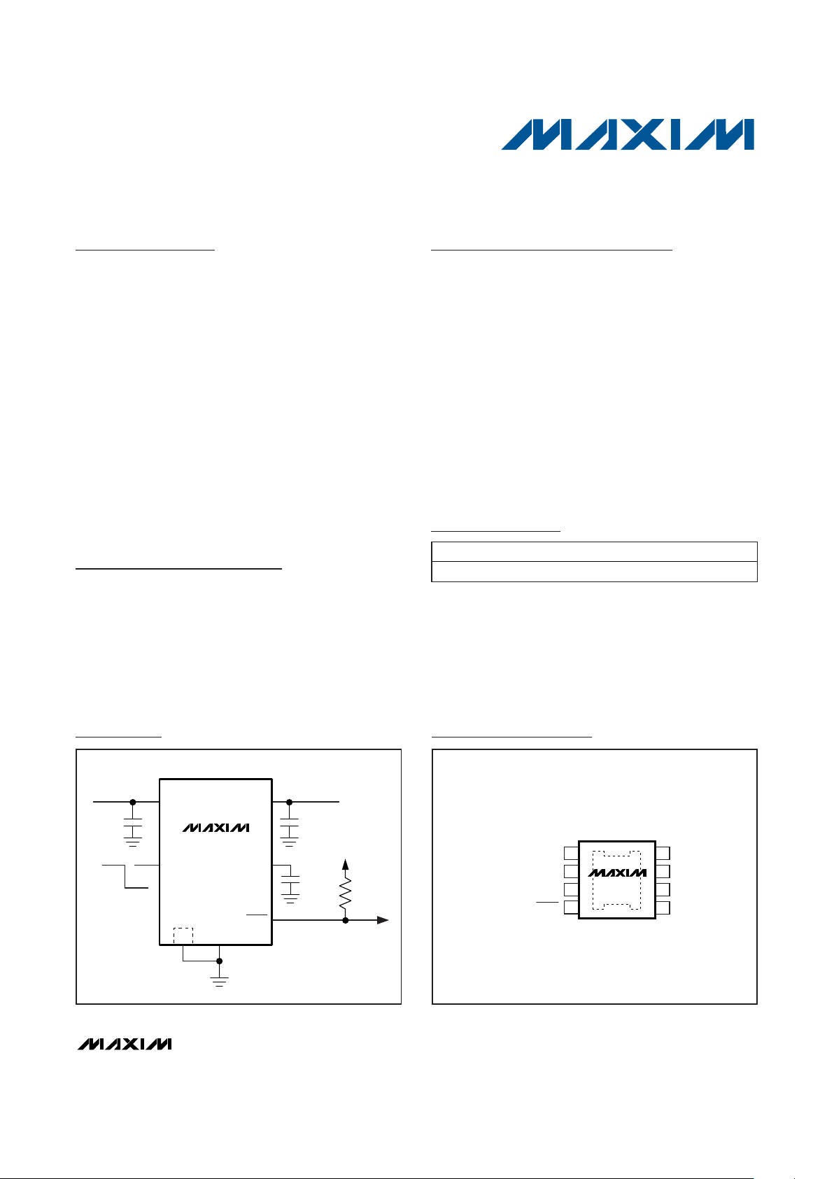
INPUT
2.5V TO 5.5V
OUTPUT
0.5V TO 3.3V
ON
C
IN
1μF
OFF
TO CONTROLLER
GND
IN
OUT
CRES
RESET
EN
EP
LOGIC
SUPPLY
MAX16999
C
OUT
4.7μF
C
CRES
15nF
Typical Operating Circuit
19-4114; Rev 0; 4/08
For pricing, delivery, and ordering information, please contact Maxim Direct at 1-888-629-4642,
or visit Maxim’s website at www.maxim-ic.com.
Ordering Information
*
Insert the desired two-digit suffix (see the Selector Guide) into
the blanks to complete the part number. Contact the factory for
other output voltages or other package options.
+
Denotes a lead-free package and RoHS compliant.
**
EP = Exposed pad.
PART* TEMP RANGE PIN-PACKAGE
MAX16999AUA_ _+ -40°C to +125°C 8 µMAX-EP**
1
2
3
4
+
8
7
6
5
IN
IN
EN
GND
*EXPOSED PAD
*
RESET
CRES
OUT
OUT
MAX16999
μMAX
TOP VIEW
Pin Configuration
Selector Guide appears at end of data sheet.
µMAX is a registered trademark of Maxim Integrated Products, Inc.

MAX16999
Ultra-Low Output Voltage, Low-Quiescent-Current
Linear Regulator for High-Temperature Applications
2 _______________________________________________________________________________________
ABSOLUTE MAXIMUM RATINGS
DC ELECTRICAL CHARACTERISTICS
(For devices with V
OUT
≤ 1.5V, VIN= 3.3V. For devices with V
OUT
> 1.5V, VIN= 5V. EN = IN, TJ= -40°C to +125°C, CIN= 1µF, C
OUT
= 4.7µF, C
CRES
= 1000pF, unless otherwise noted. Typical values are at TA= +25°C.) (Note 1)
Stresses beyond those listed under “Absolute Maximum Ratings” may cause permanent damage to the device. These are stress ratings only, and functional
operation of the device at these or any other conditions beyond those indicated in the operational sections of the specifications is not implied. Exposure to
absolute maximum rating conditions for extended periods may affect device reliability.
IN, RESET to GND.................................................-0.3V to +6.0V
OUT, CRES, EN to GND ..............................-0.3V to (V
IN
+ 0.3V)
Output Short-Circuit Duration.....................................Continuous
Continuous Power Dissipation (T
A
= +70°C) (Note 1)
(derate 10.3mW/°C above +70°C)
8-Pin µMAX (single-layer PCB) ..................................824.7mW
(derate 12.9mW/°C above +70°C)
8-Pin µMAX (multilayer PCB)....................................1030.9mW
Package Junction-to-Case Thermal Resistance (θ
JC
) ......4.8°C/W
Package Junction-to-Ambient Thermal Resistance (θ
JA
)
(single-layer PCB) ........................................................97°C/W
Package Junction-to-Ambient Thermal Resistance (θ
JA
)
(multilayer PCB) ........................................................77.6°C/W
Operating Temperature Range .........................-40°C to +125°C
Junction Temperature......................................................+150°C
Storage Temperature Range .............................-60°C to +150°C
Lead Temperature (soldering, 10s) .................................+300°C
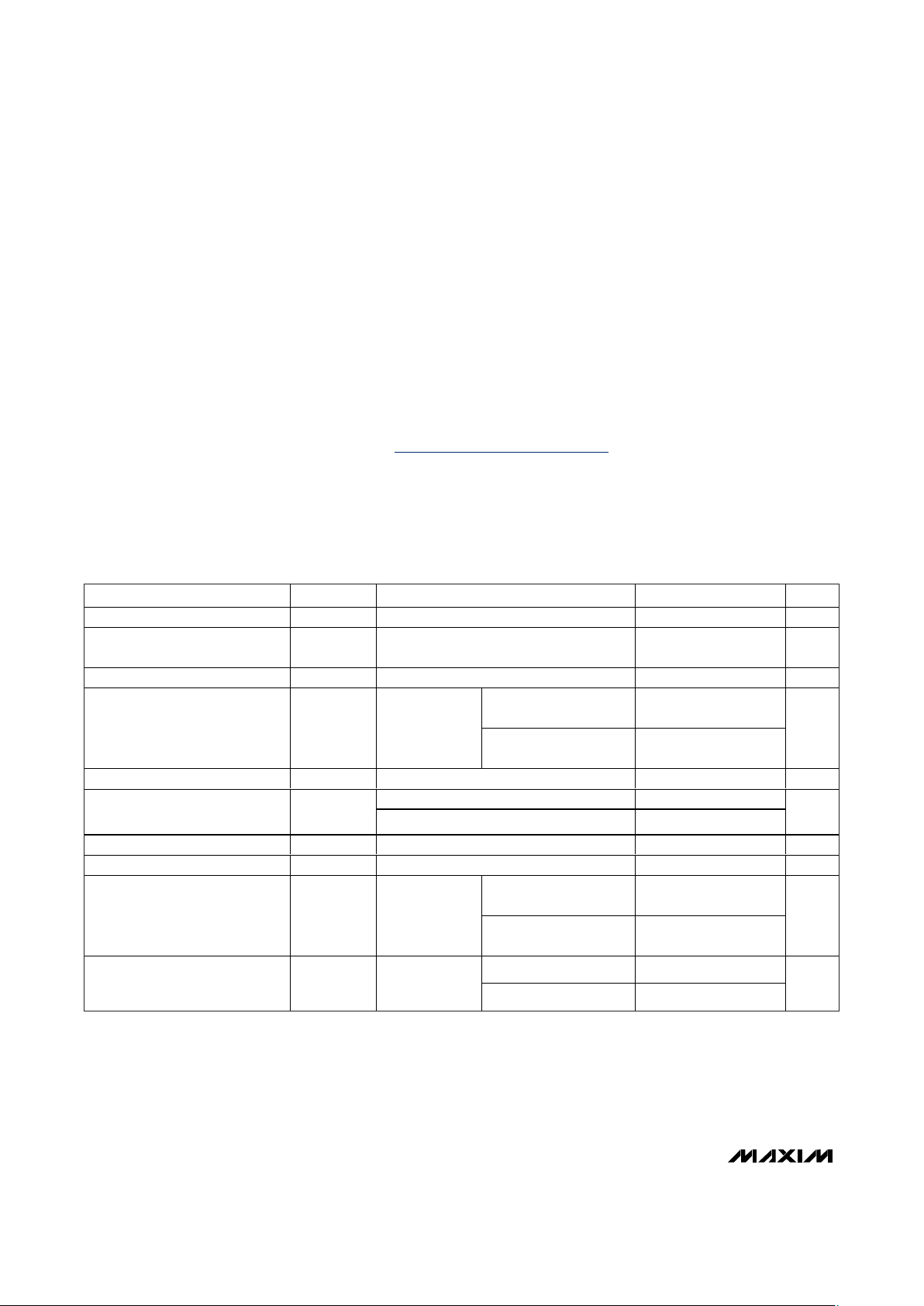
PARAMETER SYMBOL CONDITIONS MIN TYP MAX UNITS
IN Operating Voltage V
IN
2.5 5.5 V
IN Undervoltage-Lockout (UVLO)
Threshold
V
UVLO
VIN rising 1.94 2.2 V
IN UVLO Hysteresis 45 mV
V
OUT
≤ 1.5V,
I
OUT
= 1mA to 80mA
-2.5 +2.5
Output-Voltage Accuracy VIN = V
OUT
+ 2V
V
OUT
> 1.5V,
I
OUT
= 1mA to 100mA
-2.5 +2.5
%
Current Limit I
LIM
OUT = GND 105 150 mA
I
OUT
= 100µA 13 20
Ground Current I
Q
I
OUT
= 100mA 23
µA
Dropout Voltage VIN - V
OUTIOUT
= 80mA, V
OUT
= 3.3V (Note 2) 0.035 0.1 V
Load Regulation ΔV
OUT
/ΔI
OUTIOUT
= 1mA to 80mA 0.1 mV/mA
V
OUT
< 1V,
2.5V < V
IN
< 5.5V
0.4
Line Regulation ΔV
OUT
/ΔVINI
OUT
= 80mA
V
OUT
≥ 1V, (V
OUT
+
1.5V) < V
IN
< 5.5V
1.8
mV/V
f = 100Hz 70
Power-Supply Rejection Ratio PSRR
I
OUT
= 10mA,
500mV
P-P, VIN
-
V
OUT
> 1.5V
f = 100kHz 40
dB
Note 1: Package thermal resistances were obtained using the method described in JEDEC specifications. For detailed information
on packaging thermal considerations, refer to www.maxim-ic.com/thermal-tutorial
.

MAX16999
Ultra-Low Output Voltage, Low-Quiescent-Current
Linear Regulator for High-Temperature Applications
_______________________________________________________________________________________ 3
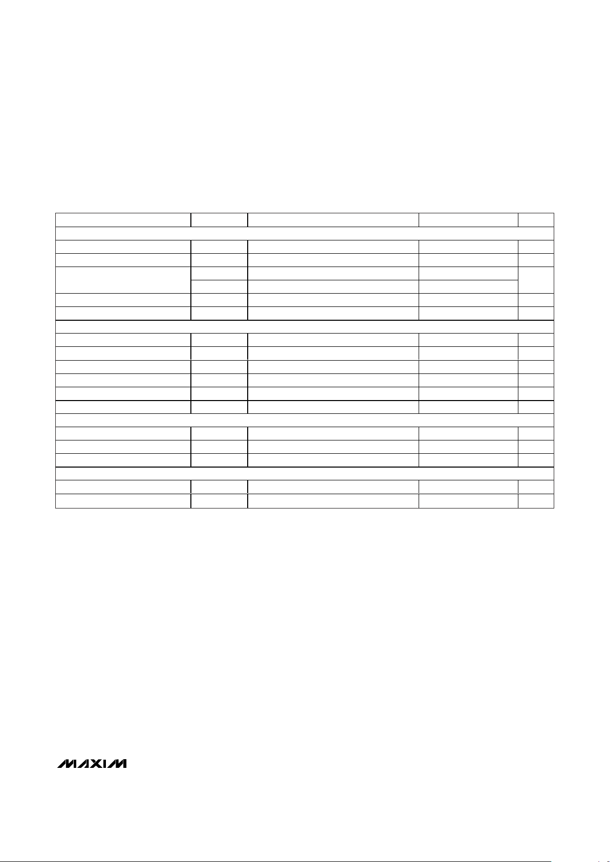
Note 2: Limits are 100% production tested at TA= +25°C. Limits over the operating temperature range are guaranteed by design.
Note 3: Dropout voltage is defined as V
IN
- V
OUT
when V
OUT
is 2% below its value for VIN= V
OUT
+ 2V.
DC ELECTRICAL CHARACTERISTICS (continued)
(For devices with V
OUT
≤ 1.5V, VIN= 3.3V. For devices with V
OUT
> 1.5V, VIN= 5V. EN = IN, TJ= -40°C to +125°C, CIN= 1µF, C
OUT
= 4.7µF, C
CRES
= 1000pF, unless otherwise noted. Typical values are at TA= +25°C.) (Note 1)
PARAMETER SYMBOL CONDITIONS MIN TYP MAX UNITS
EN
Standby Current I
STB
EN = GND 0.3 1 µA
Turn-On Delay From EN = high to V
OUT
= 100mV 10 µs
EN
H
Circuit active 70
Logic Levels
EN
L
Circuit inactive 30
%V
IN
Pullup Resistance R
EN-H
VEN = 75% V
IN
120 kΩ
Pulldown Resistance R
EN-L
VEN = 25% V
IN
120 kΩ
RESET
Threshold Accuracy V
RES
V
OUT
falling 79.5 82.5 85.5 %V
OUT
Threshold Hysteresis V
RES,HYST
2.5 %V
OUT
RESET Open-Drain Leakage RESET = high impedance, V
RESET
= 5mV 200 nA
Output Low Voltage V
RES,OLILOAD
= 250µA 100 mV
RESET T i m e o u t t
R S OF F
CRES = GND 30 80 m s
O u tp u t D eg l i t c h T i m e t
D E GL I T C H VOUT
< V
RES
30 µs
C R ES
Charge Current I
CRES,UP
81012µA
Discharge Current I
CRES,DN
1mA
Threshold V
CRES,THRS
RESET goes from low to high impedance 575 600 625 mV
T H E R M A L P R O T E C T I O N
T h er m al - S h u td o w n Te m p er a tu r e T
S H D N
+ 1 65 ° C
Thermal-Shutdown Hysteresis ΔT
S H D N
1 5 ° C
 Loading...