

General Description
The MAX1698 is the most efficient driver for white or
color LEDs. The device is ideal for LED backlit displays
in PDAs and digital cameras, and can also be used for
larger displays like those in laptop computers. Its
numerous benefits include greater simplicity, lower
cost, higher efficiency, longer bulb life, and greater reliability when compared to fluorescent (CCFL) and electroluminescent (EL) lamps.
The MAX1698 is a switch-mode boost controller in
which LED current, rather than output voltage, provides
the feedback signal. It can operate with battery inputs
as low as 0.8V. The device drives series-connected
LEDs with a controlled current that is measured at a
sense resistor connected at the feedback pin. The
required sense resistor is typically 15Ω, not an expensive fractional-ohm value. LED current control and dimming are accomplished with an adjust input (ADJ), not
with lossy current-limiting resistors. For larger light output, multiple LED banks can be connected in parallel
with up to 5W total output power.
The MAX1698 is supplied in a space-saving 10-pin
µMAX package that occupies half the space of an 8-pin
SO. An evaluation kit (MAX1698EVKIT) is available to
speed designs.
Applications
Battery-Powered Backlight Applications
Backlight for LCD Panels
Cell Phones
Handy Terminals
PDAs
Features
♦ Over 90% Efficiency
♦ Lossless, Adjustable LED Brightness
♦ Space-Saving 10-Pin µMAX Package
♦ Simpler, Lower Cost, More Reliable Compared
to CCFL or EL Backlights
♦ Up to 5W Output Power
MAX1698
High-Efficiency Step-Up
Current Regulator for LEDs
________________________________________________________________ Maxim Integrated Products 1
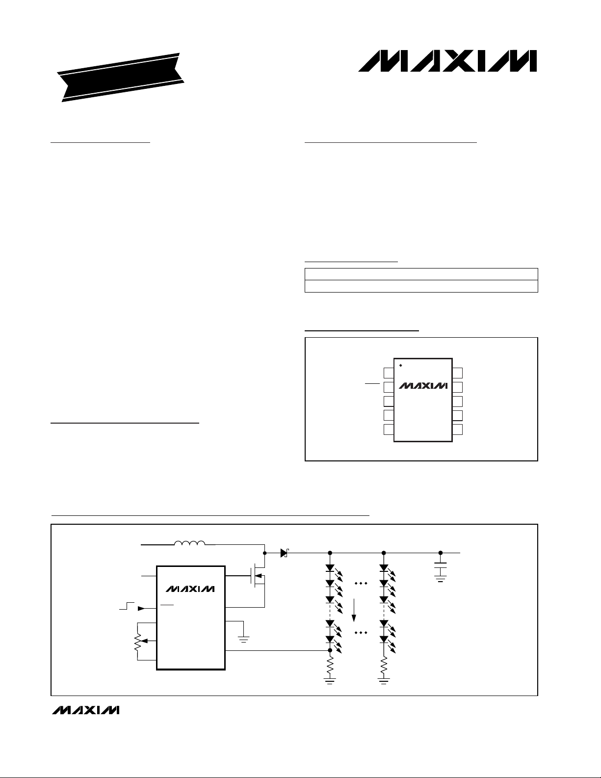
Typical Operating Circuit
19-1621; Rev 0; 1/00
PART
MAX1698EUB
-40°C to +85°C
TEMP. RANGE PIN-PACKAGE
10 µMAX
EVALUATION KIT
AVAILABLE
Pin Configuration
Ordering Information
For free samples and the latest literature, visit www.maxim-ic.com or phone 1-800-998-8800.
For small orders, phone 1-800-835-8769.
TOP VIEW
V
SHDN
REF
1
CC
2
MAX1698
3
4
5
10
9
8
7
6
EXT
CS
PGND
GNDADJ
FBGND
V
CC
SHDN
REF
ADJ
GND
L
EXT
MAX1698
CS
PGND
FB
V
BATT
V
CC
OFF
ON
µMAX
D1
I
LED
R
FB
R
N
V
OUT
C
OUT
MAX1698
High-Efficiency Step-Up
Current Regulator for LEDs
2 _______________________________________________________________________________________
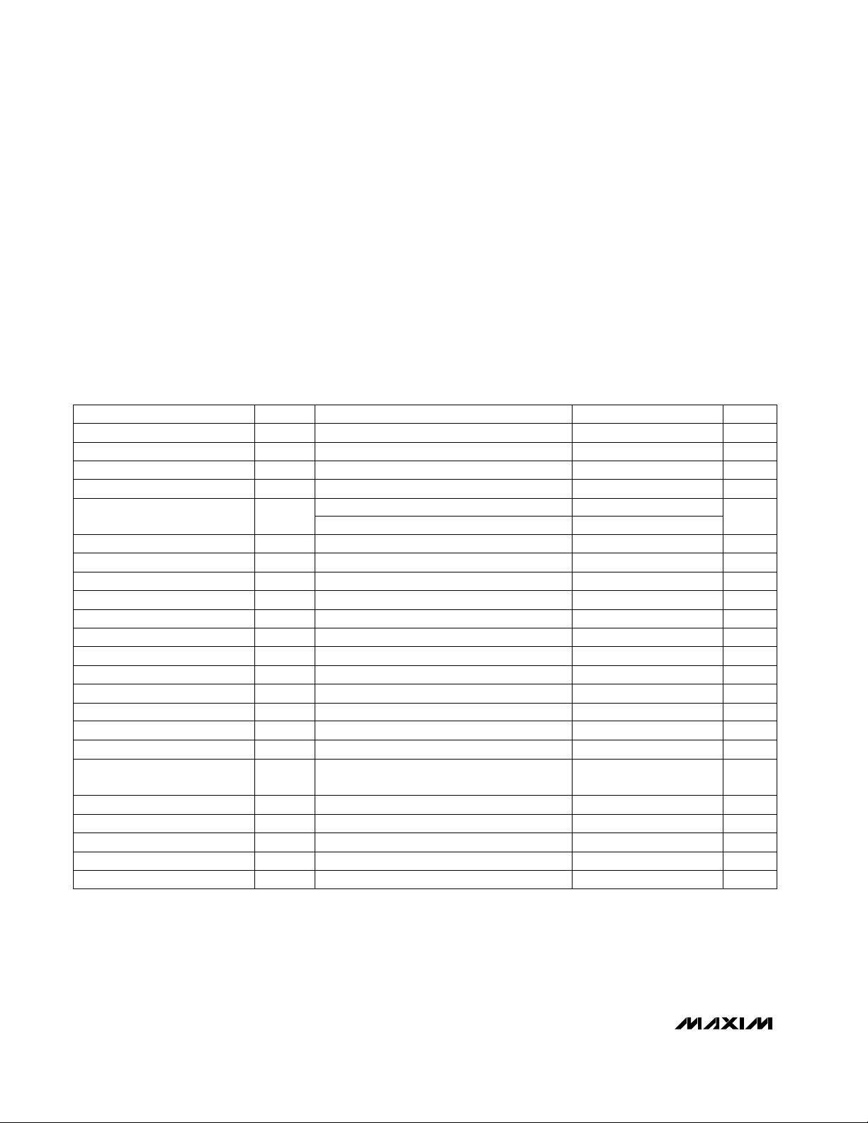
ABSOLUTE MAXIMUM RATINGS
ELECTRICAL CHARACTERISTICS
(VCC= +3.3V, TA= 0°C to +85°C, unless otherwise noted. Typical values are at TA= +25°C.)
Stresses beyond those listed under “Absolute Maximum Ratings” may cause permanent damage to the device. These are stress ratings only, and functional
operation of the device at these or any other conditions beyond those indicated in the operational sections of the specifications is not implied. Exposure to
absolute maximum rating conditions for extended periods may affect device reliability.
VCC, SHDN to GND..................................................-0.3V to +6V
EXT, FB, CS, ADJ, REF to GND..................-0.3V to (V
CC
+ 0.3V)
GND to PGND.....................................................................±0.3V
Continuous Power Dissipation (T
A
= +70°C)
10-Pin µMAX (derate 5.6mW/°C above +70°C) ............444mW
Operating Temperature Range ...........................-40°C to +85°C
Junction Temperature......................................................+150°C
Storage Temperature Range .............................-65°C to +150°C
Lead Temperature Range (soldering, 10s)......................+300°C
FB = GND, ADJ = REF, CS = GND
FB = GND, ADJ = REF
Rising edge
FB = GND
VFB= 0.3V
ADJ = REF
V
ADJ
= 100mV
CONDITIONS
mV30 50 70ADJ Start Threshold
µs10 15 20t
ON(MAX)
Maximum On Time
µs0.8 1.0 1.2t
OFF(MIN)
Minimum Off Time
A
RMS
0.8I
CS
CS Input Current
A0.8 1.5 2.5CS Trip Current
V2.25 2.4 2.55Undervoltage Lockout
µA260 500I
CC
V2.7 5.5V
CC
Supply Voltage
Quiescent Supply Current
mV80Undervoltage Hysteresis
285 300 315
mV
18 24 30
V
FB
FB Regulation Voltage
UNITSMIN TYP MAXSYMBOLPARAMETER
VFB= 300mV nA-15 15I
FB
FB Input Bias Current
V0.03 REFV
ADJ
ADJ Input Range
ADJ Input Bias Current I
ADJ
ADJ = REF -50 50 nA
Shutdown Supply Current
SHDN = GND
0.01 1 µA
REF Output Voltage V
REFIREF
= 0 1.20 1.25 1.30 V
REF Load Regulation ∆V
REFIREF
= 0 to 150µA -2 -25 mV
REF Short-Circuit Current REF = GND 0.45 1 mA
REF Power-Supply Rejection
Ratio
PSRR VCC= 2.7V to 5.5V +0.3 +2 mV/V
EXT Driver Sink/Source Current VCC= 5V, EXT = 2V 0.2 A
EXT Driver On-Resistance VCC= 5V 8 Ω
SHDN Input High Voltage
V
IH
VCC= 2.7V to 5.5V 2 V
SHDN Input Low Voltage
V
IL
VCC= 2.7V to 5.5V 0.8 V
SHDN Input Bias Current
I
SHDN
VCC= 2.7V to 5.5V -1 1 µA
MAX1698
High-Efficiency Step-Up
Current Regulator for LEDs
_______________________________________________________________________________________ 3
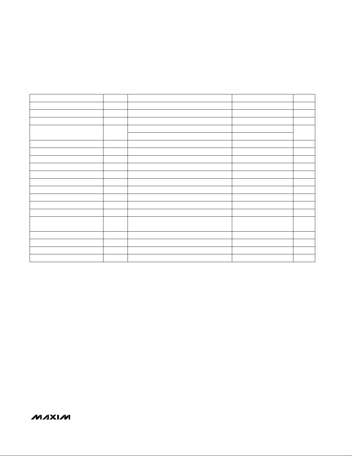
ELECTRICAL CHARACTERISTICS
(VCC= +3.3V, TA= -40°C to +85°C, unless otherwise noted.) (Note 1)
CONDITIONS
VV
CC
Supply Voltage 2.7 5.5
UNITSMIN MAXSYMBOLPARAMETER
CS Trip Current FB = GND 0.8 3.0 A
Minimum Off Time t
OFF(MIN)
FB = GND, ADJ = REF 0.6 1.4 µs
Maximum On Time t
ON(MAX)
FB = GND, ADJ = REF, CS = GND 921µs
ADJ Start Threshold 25 75 mV
FB Input Bias Current I
FB
VFB= 300mV -20 20 nA
ADJ Input Bias Current I
ADJ
ADJ = REF -50 50 nA
Shutdown Supply Current
SHDN = GND
1 µA
REF Output Voltage V
REFIREF
= 0 1.17 1.33 V
REF Load Regulation ∆V
REFIREF
= 0 to 150µA -30 mV
REF Short-Circuit Current REF = GND 1 mA
REF Power-Supply Rejection
Ratio
PSRR VCC= 2.7V to 5.5V +2 mV/V
EXT On-Resistance VCC= 5V 8 Ω
SHDN Input High Voltage
V
IH
VCC= 2.7V to 5.5V 2 V
SHDN Input Low Voltage
V
IL
VCC= 2.7V to 5.5V 0.8 V
SHDN Input Bias Current
I
SHDN
VCC= 2.7V to 5.5V -1 1 µA
Note 1: Specifications to -40°C are guaranteed by design, not production tested.
Rising edge VUndervoltage Lockout 2.20 2.65
V
ADJ
= 100mV
ADJ = REF
mV
13 35
V
FB
FB Regulation Voltage
280 320
VFB= 0.3V µAI
CC
Quiescent Supply Current 500

MAX1698
High-Efficiency Step-Up
Current Regulator for LEDs
4 _______________________________________________________________________________________
(pF)
Typical Operating Characteristics
(Circuit of Figure 2, VCC= V
BATT
= 3.3V, V
ADJ
= V
REF
, TA= +25°C, unless otherwise noted.)
OUTPUT CURRENT vs. V
25
vs. V
BATT
20
vs. V
CC
15
10
OUTPUT CURRENT (mA)
5
0
045231 678910
V
BATT
BATTERY CURRENT
1000
900
800
700
600
(mA)
500
BATT
I
400
OUT,
I
300
200
100
0
100
90
80
70
60
50
40
EFFICIENCY (%)
30
20
10
0
vs. BATTERY VOLTAGE
I
BATT
I
OUT
0 2341 567 9810
V
BATT
EFFICIENCY vs. OUTPUT CURRENT
5253515 45 55 65 75 85
OUTPUT CURRENT (mA)
AND V
BATT
1 CHAIN OF 4 LEDs
, VCC (V)
4 CHAINS OF 4 LEDs
(V)
V
= 5V
BATT
4 CHAINS OF 4 LEDs
NORMALIZED OUTPUT CURRENT
CC
1.2
MXA1698-01
1.0
0.8
0.6
0.4
NORMALIZED OUTPUT CURRENT
0.2
0
0 0.6 0.80.2 0.4 1.0 1.2 1.4
100
90
MXA1698-04
80
70
60
50
40
RISE/FALL TIME (ns)
30
20
10
0
100 400 700 1000 1300 1600 1900 2200
vs. ADJ VOLTAGE
ADJ VOLTAGE (V)
EXT RISE/FALL TIME vs. C
RISE TIME
FALL TIME
C
EXT
EXT
MXA1698-02
MXA1698-05
22.0
21.5
21.0
OUTPUT CURRENT (mA)
20.5
20.0
0 468102 1214161820
100
90
80
70
60
50
40
EFFICIENCY (%)
30
20
10
0
0426810
OUTPUT CURRENT
vs. INPUT VOLTAGE
1 CHAIN OF 4 LEDs
INPUT VOLTAGE (V)
EFFICIENCY vs. BATTERY VOLTAGE
I
= 80mA
OUT
4 CHAINS OF 4 LEDs
BATTERY VOLTAGE (V)
MXA1698-03
MXA1698-06
LED AND INDUCTOR CURRENT
MXA1698-07
SHUTDOWN/SOFT-START TIMING
3.3V
0
I
SET TO 80mA,
OUT
5ms/div
MXA1698-08
4 CHAINS OF 4 LEDs
I
OUT
50mA/div
I
BATT
100mA/div
SHDN
5V/div
WAVEFORMS
1µs/div
MXA1698-09
LED
CURRENT
50mA/div
INDUCTOR
CURRENT
500mA/div

MAX1698
High-Efficiency Step-Up
Current Regulator for LEDs
_______________________________________________________________________________________ 5
NAME FUNCTION
1 V
CC
IC Supply Voltage Input. Power for internal circuitry. Input range is 2.7V to 5.5V.
2
SHDN
Active-Low Shutdown Input. In shutdown, the MOSFET turns off, but a current path still exists between the
input and output. The minimum forward voltage of the LED array must exceed the maximum V
BATT
to ensure
that the LEDs are off in shutdown.
PIN
3 REF
1.25V Reference Output. Capable of sourcing 150µA for external loads. This pin is internally compensated.
Do not connect any bypass capacitors at REF.
4 ADJ Adjust Input. Allows dynamic adjustment of the output current. FB regulates to 300mV when ADJ = REF.
6 FB Feedback Input. Connect to the external LED current-sense feedback resistor.
8 PGND Power Ground
9 CS FET Current-Sense Input
5, 7 GND Ground
10 EXT Gate Driver Output
Pin Description
UNDERVOLTAGE
LOCKOUT/
SHUTDOWN
CS
PGND
EXT
REF
GND
ADJ
FB
SHDN
V
L
V
CC
V
CC
MAX t
ON
MIN t
OFF
MAX1698
SOFT-START
1.25V REFERENCE
Figure 1. Functional Diagram

MAX1698
High-Efficiency Step-Up
Current Regulator for LEDs
6 _______________________________________________________________________________________
Detailed Description
The MAX1698’s high efficiency and small size make it
ideally suited to drive LEDs. It operates as a boost DCDC converter that controls output current rather than
voltage. Losses are minimized by a low, 300mV current-sense threshold. In the standard configuration, a
feedback resistor, RFB, sets the current through the primary chain of LEDs. Additional chains of matching
LEDs can be added with an equivalent resistor. In
matched LED arrays, the secondary chain currents
closely track the primary chain. An optional zener
diode, D2, prevents overvoltage in the event that one of
the LEDs in the primary chain becomes an open circuit.
The LED brightness can be adjusted dynamically by a
voltage input at ADJ.
Shutdown
In shutdown, the MAX1698’s supply current is reduced
below 1µA. EXT goes low in shutdown, shutting off the
external N-channel FET. This leaves a current path
between the input and the LEDs through the boost
inductor and catch diode. The minimum forward voltage of the LED array must exceed the maximum V
BATT
to ensure that the LEDs remain off in shutdown. Typical
shutdown timing characteristics are shown in the
Typical Operating Characteristics.
Soft-Start
The MAX1698 includes a soft-start function that eliminates input current surges at turn-on. It does this by
extending the external FET driver (EXT) minimum offtime during start-up. During the first 512 switching
cycles, the minimum off-time is 5µs. It is then allowed to
drop to 2µs for the next 1500 switching cycles. After
that time, the minimum off-time falls to the 1µs value
used during normal operation. (See Shutdown/SoftStart Timing in the Typical Operating Characteristics
section.)
Design Procedure
Setting the Maximum LED Current
Resistor RFBsets the maximum current in the primary
chain of LEDs:
where I
LEDMAX
is the maximum LED current.
Adjusting LED Current
RFBsets the maximum LED current. This current can
be reduced proportional to the voltage at the ADJ pin
(see Normalized Output Current vs. ADJ Voltage in the
Typical Operating Characteristics section). Figure 3
Figure 2. Typical Operating Circuit
10µH
V
= 3.3V
BATT
10µF
VCC = 3.3V
1µF
V
CC
SHDN
REF
ADJ
MAX1698
GND
EXT
CS
FB
PGND
MBR0540
OPTIONAL
DZ
15Ω 15Ω 15Ω 15Ω
R
FB
1µF
LEDs
R
=
FB
mV
300
I
LEDMAX

MAX1698
High-Efficiency Step-Up
Current Regulator for LEDs
_______________________________________________________________________________________ 7
shows the standard method of setting the ADJ voltage.
Use the following equation to determine I
LED
:
where V
ADJ
is the voltage at ADJ. Note that ADJ volt-
ages below 50mV turns the LEDs off.
Inductor Selection
Choose an inductor with low DC resistance (in the
neighborhood of 100mΩ) to minimize losses. A typical
inductance value for L is 10µH; however, values from
3.3µH to 100µH can also be used. Higher inductor values will reduce the MAX1698’s switching frequency.
The typical operating frequency is given by:
The MAX1698 limits peak inductor current to 1.5A, but
also contains a control loop that reduces inductor current as a function of output power. For a given output
power, the required inductor peak current rating is
approximately set by:
I
L(PEAK)
= 1.0 · P
OUT
where P
OUT
is the output power to all LED banks in
watts and I
L(PEAK)
is in amperes.
Capacitor Selection
The exact value of output capacitance is not critical.
Typical values for the output capacitor are 0.1µF to
10µF. Larger values help reduce output ripple at the
expense of size and higher cost.
The requirements of the input capacitor depend on the
type of the input voltage source. However, in many
applications, the same capacitor type and value are
used for both the input and output capacitors.
Transistor Selection
The MAX1698 drives an external N-channel MOSFET.
Since the gate drive voltage is derived from VCC, best
performance is achieved with low-threshold NFETs that
specify on-resistance with gate-source voltages (VGS)
at the voltage supplied at VCCor less. For best results,
minimize the FET’s R
DS(ON)
. The external NFET’s maxi-
mum drain-to-source voltage (V
DS(MAX)
) must exceed
the output voltage.
Catch Diode (D1) Selection
The MAX1698’s high switching frequency demands a
high-speed rectifier. Schottky diodes are recommended for most applications, due to their fast recovery time
and low forward-voltage drop. Ensure that the diode’s
average and peak current ratings exceed the average
output current and peak inductor current, respectively.
In addition, the diode’s reverse breakdown voltage
must exceed V
OUT
. For output voltages exceeding 40V,
high-speed silicon rectifiers may be required for their
higher breakdown voltages.
Zener Diode
For applications requiring open-circuit protection if one
of the LEDs in the primary chain opens, add a zener
diode as shown in Figure 2. The zener diode protects
the MOSFET and output capacitor if the current feedback signal is lost. The zener voltage should exceed
the maximum forward voltage of the LED network by at
least 2V.
Applications Information
PC Board Layout
Due to fast switching waveforms and high-current
paths, careful PC board layout is required. Protoboards
and wire-wrap boards should not be used for evaluation. An EV kit (MAX1698EVKIT) is available to aid most
designs.
When laying out a board, minimize trace lengths to CS,
the inductor, diode, input capacitor, and output capacitor. Keep traces short, direct, and wide. Keep noisy
traces such as the inductor’s traces away from FB.
VCC’s bypass capacitor should be placed as close to
the IC as possible.
Refer to the MAX1698 EV kit for an example of proper
layout.
Figure 3. Adjusting LED Current
TRANSISTOR COUNT: 2180
Chip Information
REF
MAX1698
I
LED
ADJ
GND
V
ADJ
.
=⋅416
R
FB
500k
f
=
⋅067
.
V
L
BATT

MAX1698
High-Efficiency Step-Up
Current Regulator for LEDs
Maxim cannot assume responsibility for use of any circuitry other than circuitry entirely embodied in a Maxim product. No circuit patent licenses are
implied. Maxim reserves the right to change the circuitry and specifications without notice at any time.
8 _____________________Maxim Integrated Products, 120 San Gabriel Drive, Sunnyvale, CA 94086 408-737-7600
© 2000 Maxim Integrated Products Printed USA is a registered trademark of Maxim Integrated Products.
Package Information
Note: The MAX1698 does not have an exposed pad.
10LUMAX.EPS
 Loading...