

General Description
The MAX1697 ultra-small, monolithic, CMOS chargepump voltage inverter accepts an input voltage ranging
from +1.25V to +5.5V. This device features an ultra-low
12Ω output resistance, permitting loads of up to 60mA
with maximum efficiency. The MAX1697 is available
with operating frequencies of 12kHz, 35kHz, 125kHz, or
250kHz, allowing optimization of supply current or
external component size. Its small external components
and micropower shutdown mode make this device
ideal for both battery-powered and board-level voltage
conversion applications.
Oscillator control circuitry and four power MOSFET
switches are included on-chip. Applications include
generating a negative supply from a +5V or +3.3V logic
supply to power analog circuitry. All versions come in a
6-pin SOT23 package and deliver 60mA.
For applications with lower current requirements, the
MAX1719/MAX1720/MAX1721 are pin-compatible
SOT23 charge pumps that supply up to 25mA.
Applications
Negative Supply from +5V or +3.3V Logic Supplies
Small LCD Panels
GaAsFET Bias Supplies
Handy-Terminals, PDAs
Battery-Operated Equipment
Features
♦ 60mA Output Current
♦ Low 12Ω Output Resistance
♦ 150µA Supply Current (MAX1697R)
♦ Requires Only Two 1µF Capacitors (MAX1697U)
♦ Start-Up Current Limited
♦ +1.25V to +5.5V Input Voltage Range
♦ 0.1µA Logic-Controlled Shutdown
♦ Slew-Rate Limited to Reduce EMI
♦ 6-Pin SOT23 Package
MAX1697
60mA, SOT23 Inverting Charge Pump
with Shutdown
________________________________________________________________
Maxim Integrated Products
1
SHDN
5
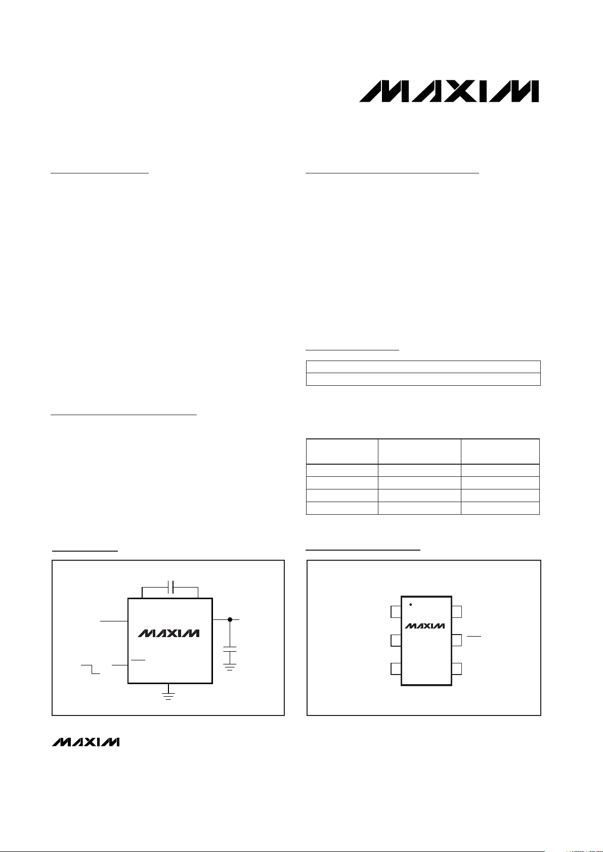
TOP VIEW
IN
GND
C1-
C1+
OUT
SOT23-6
1
6
MAX1697
2
3
4
Pin Configuration
C1+ C1-
IN
SHDN
OUT
GND
ON
1µF
1µF
OFF
INPUT
1.5V to 5.5V
NEGATIVE
OUTPUT
-1 · V
IN
60mA
MAX1697U
Typical Operating Circuit
19-1499; Rev 0; 7/99
PART
MAX1697_EUT-T
-40°C to +85°C
TEMP. RANGE PIN-PACKAGE
6 SOT23-6
Ordering Information
For free samples & the latest literature: http://www.maxim-ic.com, or phone 1-800-998-8800.
For small orders, phone 1-800-835-8769.
PART NO.
SUFFIX
R 12
FREQUENCY
(kHz)
TOP
MARK
AABV
S 35 AABW
T
U 250 AABY
125 AABX
Note: The MAX1697 is available with four different operating
frequencies. Choose the desired frequency from the table
below and insert the suffix in the blank above to complete the
part number.
MAX1697
60mA, SOT23 Inverting Charge Pump
with Shutdown
2 _______________________________________________________________________________________
ABSOLUTE MAXIMUM RATINGS
ELECTRICAL CHARACTERISTICS
(Circuit of Figure 1, capacitors from Table 2, V
IN
= +5V, SHDN = IN, TA= 0°C to +85°C, unless otherwise noted. Typical values are at
T
A
= +25°C.)
Stresses beyond those listed under “Absolute Maximum Ratings” may cause permanent damage to the device. These are stress ratings only, and functional
operation of the device at these or any other conditions beyond those indicated in the operational sections of the specifications is not implied. Exposure to
absolute maximum rating conditions for extended periods may affect device reliability.
IN to GND .................................................................-0.3V to +6V
C1+, SHDN to GND .....................................-0.3V to (V
IN
+ 0.3V)
C1- to GND..............................................(V
OUT
- 0.3V) to + 0.3V
OUT to GND .............................................................+0.3V to -6V
OUT Output Current............................................................90mA
OUT Short-Circuit to GND .............................................Indefinite
Continuous Power Dissipation (T
A
= +70°C)
6-Pin SOT23 (derate 14mW/°C above +70°C) ................1.1W
Operating Temperature Range ...........................-40°C to +85°C
Junction Temperature......................................................+150°C
Storage Temperature Range .............................-65°C to +150°C
Lead Temperature (soldering, 10sec) .............................+300°C
I
OUT
= 15mA
MAX1697T/U, R
L
= 5kΩ
SHDN = GND or IN
V
IN(MIN)
≤ VIN≤ 2.5V
MAX1697R/S, R
L
= 5kΩ
2.5V ≤ VIN≤ 5.5V
V
IN(MIN)
≤ VIN≤ 2.5V
2.5V ≤ VIN≤ 5.5V
I
OUT
= 0, TA= +25°C
SHDN = GND, OUT is internally pulled to GND
in shutdown
TA= +25°C
TA= +25°C
SHDN = GND
I
OUT
= 60mA
CONDITIONS
600
µs
1200
Wake-Up Time from Shutdown
10
nA
-100 0.05 +100
SHDN Bias Current
0.2
V
0.6
SHDN Input Logic Low
VIN- 0.2
V
2.0
SHDN Input Logic High
Ω38
OUT to GND Shutdown
Resistance
33
Ω
12 25
Output Resistance (Note 1)
1.4 5.5
1.5 5.5
V
1.25 5.5
Supply Voltage Range
%99 99.9Voltage Conversion Efficiency
20 35 50
kHzOscillator Frequency
0.03
1.5 5.5
µA
150 300
Quiescent Supply Current
350 650
µA
0.002 1
Shutdown Supply Current
UNITSMIN TYP MAXPARAMETER
TA= 0°C to + 85°C
TA= +25°C
TA= 0°C to + 85°C
TA= +25°C
MAX1697S
MAX1697R
TA= +85°C
TA= +25°C
TA= 0°C to +85°C
TA= +25°C
TA= +85°C
TA= +25°C
MAX1697S
MAX1697R
MAX1697U
MAX1697T 950 1700
1800 3400
Output shorted to ground, TA= +25°C mA170Short-Circuit Current
71217
MAX1697U 70
MAX1697T 100
140 250 360
70 125 180
MAX1697R
MAX1697S
MAX1697T
MAX1697U
MAX1697
60mA, SOT23 Inverting Charge Pump
with Shutdown
_______________________________________________________________________________________
3
ELECTRICAL CHARACTERISTICS
(Circuit of Figure 1, capacitors from Table 2, V
IN
= +5V, SHDN = IN, TA= -40°C to +85°C, unless otherwise noted.) (Note 2)
ELECTRICAL CHARACTERISTICS (continued)
(Circuit of Figure 1, capacitors from Table 2, V
IN
= +5V, SHDN = IN, TA= 0°C to +85°C, unless otherwise noted. )Typical values are at
T
A
= +25°C.)
CONDITIONS
150
UNITSMIN TYP MAXPARAMETER
Note 1: Output resistance is guaranteed with capacitor ESR of 0.3Ω or less.
Note 2: All specifications from -40°C to +85°C are guaranteed by design, not production tested.
Trip Temperature °C
Hysteresis °C15
Temperature increasing
THERMAL SHUTDOWN
VR
L
= 5kΩSupply Voltage Range
1.6 5.5
MAX1697R
V
IN(MIN)
≤ VIN≤ 2.5V
2.5V ≤ VIN≤ 5.5V
V
IN(MIN)
≤ VIN≤ 2.5V
2.5V ≤ VIN≤ 5.5V
MAX1697T/U
1.5 5.5
µA
SHDN = GND, OUT is internally pulled to GND in
shutdown
350
Continuous, long-term
Quiescent Current
750
MAX1697T
MAX1697R
I
OUT
= 60mA
CONDITIONS
1800
kHz
621
3600
MAX1697S
MAX1697U
Oscillator Frequency
16 60
MAX1697T 60 200
120 400
MAX1697S
MAX1697U
MAX1697R/S
0.2
V
0.6
SHDN Input Logic Low
VIN- 0.2
V
2.1
SHDN Input Logic High
Ω8
OUT to GND Shutdown
Resistance
33 ΩOutput Resistance (Note 1)
mA
RMS
60Output Current
UNITSMIN MAXPARAMETER
0
10
15
25
20
30
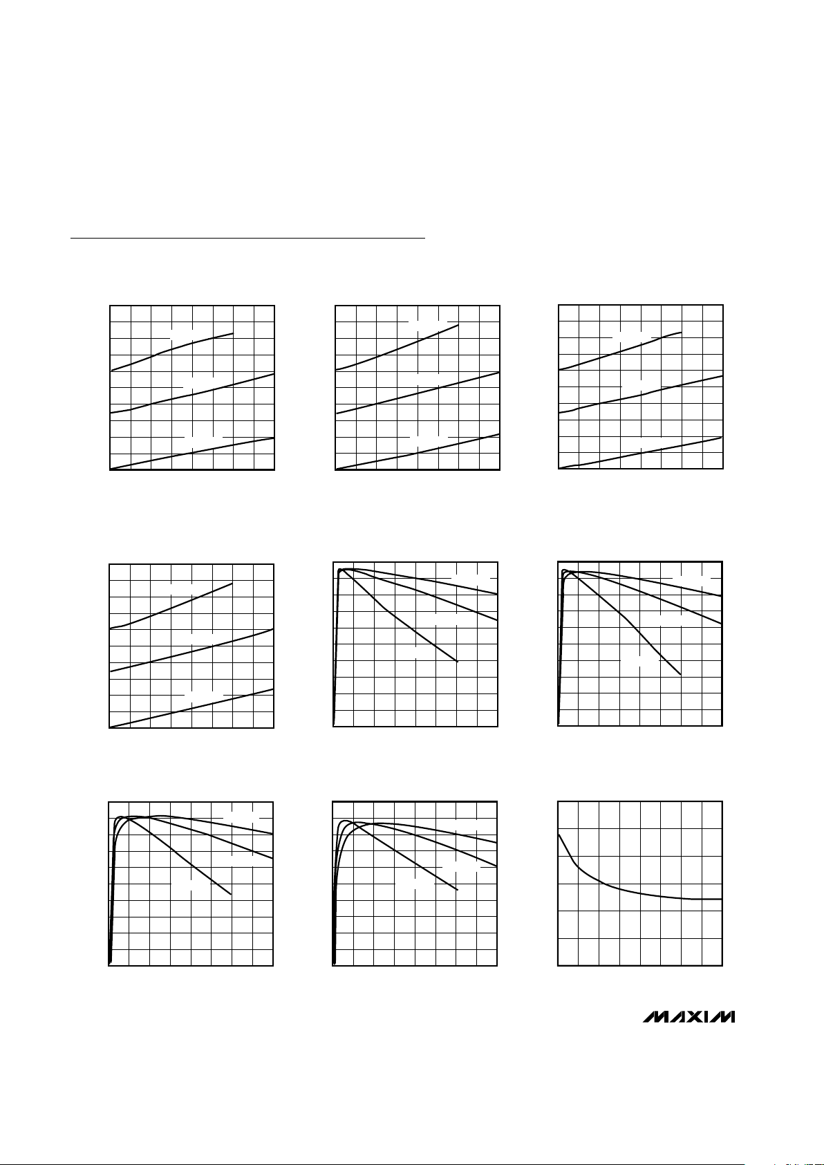
1.5 2.5 3.02.0 3.5 4.0 4.5 5.0 5.5
MAX1697R/S/T/U
OUTPUT IMPEDANCE vs. INPUT VOLTAGE
MAX1697 TOC09
INPUT VOLTAGE (V)
OUTPUT IMPEDANCE (Ω)
5
0
20
10
40
30
60
50
70
90
80
100
0203010 40 50 60 70 80
MAX1697U
EFFICIENCY vs. OUTPUT CURRENT
MAX1697 TOC08
OUTPUT CURRENT (mA)
EFFICIENCY (%)
VIN = +2V
VIN = +5V
VIN = +3.3V
MAX1697
4 _______________________________________________________________________________________
0
20
10
40
30
60
50
70
90
80
100
0203010 40 50 60 70 80
MAX1697T
EFFICIENCY vs. OUTPUT CURRENT
MAX1697 TOC07
OUTPUT CURRENT (mA)
EFFICIENCY (%)
VIN = +2V
VIN = +5V
VIN = +3.3V
-5.0
-4.0
-4.5
-3.0
-3.5
-2.0
-2.5
-1.5
-0.5
-1.0
0
0203010 40 50 60 70 80
MAX1697R
OUTPUT VOLTAGE
vs. OUTPUT CURRENT
MAX1697 TOC01
OUTPUT CURRENT (mA)
OUTPUT VOLTAGE (V)
VIN = +2V
VIN = +5V
VIN = +3.3V
-5.0
-4.0
-4.5
-3.0
-3.5
-2.0
-2.5
-1.5
-0.5
-1.0
0
0203010 40 50 60 70 80
MAX1697U
OUTPUT VOLTAGE
vs. OUTPUT CURRENT
MAX1697 TOC04
OUTPUT CURRENT (mA)
OUTPUT VOLTAGE (V)
VIN = +2V
VIN = +5V
VIN = +3.3V
-5.0
-4.0
-4.5
-3.0
-3.5
-2.0
-2.5
-1.5
-0.5
-1.0
0
0203010 40 50 60 70 80
MAX1697S
OUTPUT VOLTAGE
vs. OUTPUT CURRENT
MAX1697 TOC02
OUTPUT CURRENT (mA)
OUTPUT VOLTAGE (V)
VIN = +2V
VIN = +5V
VIN = +3.3V
-5.0
-4.0
-4.5
-3.0
-3.5
-2.0
-2.5
-1.5
-0.5
-1.0
0
0203010 40 50 60 70 80
MAX1697T
OUTPUT VOLTAGE
vs. OUTPUT CURRENT
MAX1697 TOC03
OUTPUT CURRENT (mA)
OUTPUT VOLTAGE (V)
VIN = +2V
VIN = +5V
VIN = +3.3V
0
20
10
40
30
60
50
70
90
80
100
0203010 40 50 60 70 80
MAX1697R
EFFICIENCY vs. OUTPUT CURRENT
MAX1697 TOC05
OUTPUT CURRENT (mA)
EFFICIENCY (%)
VIN = +2V
VIN = +5V
VIN = +3.3V
0
20
10
40
30
60
50
70
90
80
100
0203010 40 50 60 70 80
MAX1697S
EFFICIENCY vs. OUTPUT CURRENT
MAX1697 TOC06
OUTPUT CURRENT (mA)
EFFICIENCY (%)
VIN = +2V
VIN = +5V
VIN = +3.3V
Typical Operating Characteristics
(Circuit of Figure 1, capacitors from Table 2, VIN= +5V, SHDN = IN, TA= +25°C, unless otherwise noted.)
60mA, SOT23 Inverting Charge Pump
with Shutdown

MAX1697
60mA, SOT23 Inverting Charge Pump
with Shutdown
_______________________________________________________________________________________
5
0
0.5
1.0
2.0
1.5
2.5
1.5 2.5 3.02.0 3.5 4.0 4.5 5.0 5.5
SUPPLY CURRENT
vs. INPUT VOLTAGE
MAX1697 TOC10
INPUT VOLTAGE (V)
SUPPLY CURRENT (mA)
MAX1697R
MAX1697S
MAX1697T
MAX1697U
0
5
15
10
25
20
30
35
-40 0 20-20 40 60 80
MAX1697R/S/T/U
SHUTDOWN SUPPLY CURRENT
vs. TEMPERATURE
MAX1697 TOC11
TEMPERATURE (°C)
SUPPLY CURRENT (nA)
VIN = +2V
VIN = +3.3V
VIN = +5V
0
5
15
10
25
20
30
35
-40 0 20-20 40 60 80
MAX1697R
OUTPUT RESISTANCE
vs. TEMPERATURE
MAX1697 TOC12
TEMPERATURE (°C)
OUTPUT RESISTANCE (Ω)
VIN = +2V
VIN = +1.5V
VIN = +5V
VIN = +3.3V
0
5
15
10
25
20
30
-40 0 20-20 40 60 80
MAX1697S
OUTPUT RESISTANCE
vs. TEMPERATURE
MAX1697 TOC13
TEMPERATURE (°C)
OUTPUT RESISTANCE (Ω)
VIN = +2V
VIN = +1.5V
VIN = +5V
VIN = +3.3V
1
100
10
1000
-40 -20 0 20 40 60 80
PUMP FREQUENCY
vs. TEMPERATURE
MAX1697 TOC16
TEMPERATURE (°C)
PUMP FREQUENCY (kHz)
MAX1697U
MAX1697T
MAX1697S
MAX1697R
VIN = +1.5V TO +5V
0
5
15
10
25
20
30
35
-40 0 20-20 40 60 80
MAX1697T
OUTPUT RESISTANCE
vs. TEMPERATURE
MAX1697 TOC14
TEMPERATURE (°C)
OUTPUT RESISTANCE (Ω)
VIN = +2V
VIN = +1.5V
VIN = +5V
VIN = +3.3V
0
5
15
10
25
20
30
40
35
45
-40 0 20-20 40 60 80
MAX1697U
OUTPUT RESISTANCE
vs. TEMPERATURE
MAX1697 TOC15
TEMPERATURE (°C)
OUTPUT RESISTANCE (Ω)
VIN = +2V
VIN = +1.5V
VIN = +5V
VIN = +3.3V
V
OUT
MAX1697R
(12kHz)
V
OUT
MAX1697S
(35kHz)
MAX1697R/S
OUTPUT NOISE AND RIPPLE
MAX1697 TOC17
20µs/div
V
IN
= 3.3V, I
OUT
= 5mA,
10mV/div, AC-COUPLED
V
OUT
MAX1697T
(125kHz)
V
OUT
MAX1697U
(250kHz)
MAX1697T/U
OUTPUT NOISE AND RIPPLE
MAX1697 TOC18
2µs/div
VIN = 3.3V, I
OUT
= 5mA,
10mV/div, AC-COUPLED
Typical Operating Characteristics (continued)
(Circuit of Figure 1, capacitors from Table 2, VIN= +5V, SHDN = IN, TA= +25°C, unless otherwise noted.)

MAX1697
60mA, SOT23 Inverting Charge Pump
with Shutdown
6 _______________________________________________________________________________________
Typical Operating Characteristics (continued)
(Circuit of Figure 1, capacitors from Table 2, VIN= +5V, SHDN = IN, TA= +25°C, unless otherwise noted.)
0V
SHDN
0V
MAX1697S
(35kHz)
V
OUT
, 2V/div
MAX1697R
(12kHz)
V
OUT
, 2V/div
START-UP FROM SHUTDOWN
MAX1697 TOC19
400µs/div
0V
0V
MAX1697U
(250kHz)
V
OUT
, 2V/div
MAX1697T
(125kHz)
V
OUT
, 2V/div
START-UP FROM SHUTDOWN
MAX1697 TOC20
50µs/div
SHDN
0
20
10
40
30
60
50
70
0 1015205 253035 4540 50
MAX1697R
OUTPUT CURRENT
vs. CAPACITANCE
MAX1697 TOC21
CAPACITANCE (µF)
OUTPUT CURRENT (mA)
VIN = +4.75V, V
OUT
= -4.0V
VIN = +1.9V, V
OUT
= -1.5V
VIN = +3.15V, V
OUT
= -2.5V
0
20
10
40
30
60
50
70
80
0 1015205 2530354045
MAX1697S
OUTPUT CURRENT
vs. CAPACITANCE
MAX1697 TOC22
CAPACITANCE (µF)
OUTPUT CURRENT (mA)
VIN = +1.9V, V
OUT
= -1.5V
VIN = +3.15V, V
OUT
= -2.5V
VIN = +4.75V, V
OUT
= -4.0V
0
100
50
200
150
300
250
350
450
400
500
0 1015205 253035 4540 50
MAX1697R
OUTPUT RIPPLE vs. CAPACITANCE
MAX1697 TOC25
CAPACITANCE (µF)
OUTPUT RIPPLE (mV)
VIN = +1.9V, V
OUT
= -1.5V
VIN = +3.15V, V
OUT
= -2.5V
VIN = +4.75V, V
OUT
= -4.0V
0
20
10
40
30
60
50
70
0 2341 567 9810
MAX1697T
OUTPUT CURRENT
vs. CAPACITANCE
MAX1697 TOC23
CAPACITANCE (µF)
OUTPUT CURRENT (mA)
VIN = +3.15V, V
OUT
= -2.5V
VIN = +4.75V, V
OUT
= -4.0V
VIN = +1.9V, V
OUT
= -1.5V
0
20
10
40
30
60
50
70
80
0 2341 567 9810
MAX1697U
OUTPUT CURRENT
vs. CAPACITANCE
MAX1697 TOC24
CAPACITANCE (µF)
OUTPUT CURRENT (mA)
VIN = +1.9V, V
OUT
= -1.5V
VIN = +3.15V, V
OUT
= -2.5V
VIN = +4.75V, V
OUT
= -4.0V
0
100
50
200
150
300
250
350
450
400
500
0 1015205 253035 4540 50
MAX1697S
OUTPUT RIPPLE vs. CAPACITANCE
MAX1697 TOC26
CAPACITANCE (µF)
OUTPUT RIPPLE (mV)
VIN = +1.9V, V
OUT
= -1.5V
VIN = +3.15V, V
OUT
= -2.5V
VIN = +4.75V, V
OUT
= -4.0V

Detailed Description
The MAX1697 capacitive charge pumps invert the voltage applied to their input. For highest performance, use
low equivalent series resistance (ESR) capacitors (e.g.,
ceramic).
During the first half-cycle, switches S2 and S4 open,
switches S1 and S3 close, and capacitor C1 charges to
the voltage at IN (Figure 2). During the second halfcycle, S1 and S3 open, S2 and S4 close, and C1 is level
shifted downward by VINvolts. This connects C1 in parallel with the reservoir capacitor C2. If the voltage across
C2 is smaller than the voltage across C1, charge flows
from C1 to C2 until the voltage across C2 reaches
-VIN. The actual voltage at the output is more positive
than -VIN, since switches S1–S4 have resistance and the
load drains charge from C2.
Efficiency Considerations
The efficiency of the MAX1697 is dominated by its quiescent supply current (IQ) at low output current and by
its output impedance (R
OUT
) at higher output current; it
is given by:
η≅
+
−
⋅I
II
IR
V
OUT
OUT Q
OUT OUT
IN
1
MAX1697
60mA, SOT23 Inverting Charge Pump
with Shutdown
_______________________________________________________________________________________ 7
0
100
50
200
150
300
250
350
450
400
500
0 2341 567 9810
MAX1697T
OUTPUT RIPPLE vs. CAPACITANCE
MAX1697 TOC27
CAPACITANCE (µF)
OUTPUT RIPPLE (mV)
VIN = +1.9V, V
OUT
= -1.5V
VIN = +3.15V, V
OUT
= -2.5V
VIN = +4.75V, V
OUT
= -4.0V
0
100
50
200
150
300
250
350
450
400
500
0 2341 567 9810
MAX1697U
OUTPUT RIPPLE vs. CAPACITANCE
MAX1697 TOC28
CAPACITANCE (µF)
OUTPUT RIPPLE (mV)
VIN = +1.9V, V
OUT
= -1.5V
VIN = +3.15V, V
OUT
= -2.5V
VIN = +4.75V, V
OUT
= -4.0V
Pin Description
6
Positive Terminal of the Flying
Capacitor
1
Inverting Charge-Pump Output
2
Power-Supply Voltage Input. Input
range is 1.5V to 5.5V.
3
Negative Terminal of the Flying
Capacitor
4 Ground
5
Shutdown Input. Drive this pin high
for normal operation; drive it low for
shutdown mode. OUT is actively
pulled to ground during shutdown.
PIN FUNCTIONNAME
C1+
OUT
IN
C1-
GND
SHDN
Typical Operating Characteristics (continued)
(Circuit of Figure 1, capacitors from Table 2, VIN= +5V, SHDN = IN, TA= +25°C, unless otherwise noted.)
C1
C2
21
5
ON
OFF
3
R
L
6
4
C3
C1+ C1-
IN
SHDN
OUT
GND
INPUT
1.5V to 5.5V
NEGATIVE
OUTPUT
-1 · V
IN
MAX1697
Figure 1. Typical Application Circuit

MAX1697
60mA, SOT23 Inverting Charge Pump
with Shutdown
8 _______________________________________________________________________________________
where the output impedance is roughly approximated
by:
The first term is the effective resistance of an ideal
switched-capacitor circuit (Figures 3a and 3b), and
RSWis the sum of the charge pump’s internal switch
resistances (typically 4Ω to 5Ω at V
IN
= +5V). The typical output impedance is more accurately determined
from the
Typical Operating Characteristics
.
Current Limit
The MAX1697 limits its input current upon start-up to
170mA (typ). This prevents low-current or higher output
impedance input supplies (such as alkaline cells) from
being overloaded when power is applied or when the
device awakes from shutdown.
Shutdown
The MAX1697 has a logic-controlled shutdown input.
Driving SHDN low places the device in a low-power
shutdown mode. The charge-pump switching halts,
supply current is reduced to 2nA, and OUT is actively
pulled to ground through a 3Ω resistance.
Driving SHDN high will restart the charge pump. The
switching frequency and capacitor values determine
how soon the device will reach 90% of the input voltage.
Thermal Shutdown
The MAX1697 has a thermal shutdown mode for additional protection against fault conditions. When the temperature of the die exceeds +150°C, the internal clock
stops, suspending the device’s operation. The
MAX1697 resumes operation when the die temperature
falls 15°C. This prevents the device from rapidly oscillating around the temperature trip point.
Applications Information
Capacitor Selection
The charge-pump output resistance is a function of the
ESR of C1 and C2. To maintain the lowest output resistance, use capacitors with low ESR. (See Table 1 for a
list of recommended manufacturers.) Tables 2 and 3
suggest capacitor values for minimizing output resistance or capacitor size.
Flying Capacitor (C1)
Increasing the flying capacitor’s value reduces the output resistance. Above a certain point, increasing C1’s
capacitance has negligible effect because the output
resistance is then dominated by internal switch resistance and capacitor ESR.
Output Capacitor (C2)
Increasing the output capacitor’s value reduces the
output ripple voltage. Decreasing its ESR reduces both
output resistance and ripple. Lower capacitance values
can be used with light loads if higher output ripple can
be tolerated. Use the following equation to calculate the
peak-to-peak ripple:
Input Bypass Capacitor (C3)
If necessary, bypass the incoming supply to reduce its
AC impedance and the impact of the MAX1697’s switching noise. A bypass capacitor with a value equal to that
of C1 is recommended.
V=
I
2(f )C2
2 I ESR
RIPPLE
OUT
OSC
OUT C2
+ ⋅⋅
R
1
fC1
2R 4ESR ESR
OUT
OSC
SW C1 C2
≅
()
++ +
⋅
S1
IN
S2
S3 S4
C1
C2
V
OUT
= -(VIN)
Figure 2. Ideal Voltage Inverter
V+
C1
f
OSC
C2 R
L
V
OUT
Figure 3a. Switched-Capacitor Model
R
EQUIV
=
R
EQUIV
V
OUT
R
L
1
V+
f
OSC
· C1
C2
Figure 3b. Equivalent Circuit

MAX1697
60mA, SOT23 Inverting Charge Pump
with Shutdown
_______________________________________________________________________________________ 9
Surface-Mount
Tantalum
PRODUCTION
METHOD
714-969-2491
803-946-0690
PHONE
603-224-1961 603-224-1430
714-960-6492
803-626-3123
FAXMANUFACTURER
AVX
Matsuo
Sprague
SERIES
TPS series
267 series
593D, 595D series
714-969-2491
803-946-0690AVX
Matsuo 714-960-6492
803-626-3123X7R
X7R
Surface-Mount
Ceramic
Table 2. Capacitor Selection to Minimize
Output Resistance
Table 3. Capacitor Selection to Minimize
Capacitor Size
Table 1. Low-ESR Capacitor Manufacturers
Voltage Inverter
The most common application for these devices is a
charge-pump voltage inverter (Figure 1). This application requires only two external components—capacitors
C1 and C2—plus a bypass capacitor, if necessary.
Refer to the
Capacitor Selection
section for suggested
capacitor types.
Cascading Devices
Two devices can be cascaded to produce an even
larger negative voltage (Figure 4). The unloaded output
voltage is normally -2 · V
IN
, but this is reduced slightly
by the output resistance of the first device multiplied by
the quiescent current of the second. When cascading
more than two devices, the output resistance rises dramatically. For applications requiring larger negative
voltages, see the MAX865 and MAX868 data sheets.
Paralleling Devices
Paralleling multiple MAX1697s reduces the output resistance. Each device requires its own pump capacitor
(C1), but the reservoir capacitor (C2) serves all devices
(Figure 5). Increase C2’s value by a factor of n, where
n
is the number of parallel devices. Figure 5 shows the
equation for calculating output resistance.
Combined Doubler/Inverter
In the circuit of Figure 6, capacitors C1 and C2 form the
inverter, while C3 and C4 form the doubler. C1 and C3
are the pump capacitors; C2 and C4 are the reservoir
capacitors. Because both the inverter and doubler use
part of the charge-pump circuit, loading either output
causes both outputs to decline toward GND. Make sure
the sum of the currents drawn from the two outputs
does not exceed 60mA.
Heavy Load Connected to a
Positive Supply
Under heavy loads, where a higher supply is sourcing
current into OUT, the OUT supply must not be pulled
above ground. Applications that sink heavy current into
OUT require a Schottky diode (1N5817) between GND
and OUT, with the anode connected to OUT (Figure 7).
Layout and Grounding
Good layout is important, primarily for good noise performance. To ensure good layout, mount all components as close together as possible, keep traces short
to minimize parasitic inductance and capacitance, and
use a ground plane.
MAX1697R
MAX1697S
MAX1697T
MAX1697U
12
35
125
250
22
6.8
2.2
1
12
12
12
12
PART
FREQUENCY
(kHz)
CAPACITOR
(µF)
TYPICAL
R
OUT
(Ω)
MAX1697R
MAX1697S
PART
MAX1697T
MAX1697U
FREQUENCY
(kHz)
CAPACITOR
(µF)
TYPICAL
R
OUT
(Ω)
12
35
125
250
10
3.3
1
0.47
17
17
17
17

MAX1697
60mA, SOT23 Inverting Charge Pump
with Shutdown
10 ______________________________________________________________________________________
MAX1697
2
5
1
V
OUT
= (2VIN) -
(V
FD1
) - (V
FD2
)
C2
+V
IN
C1
3
4
6
V
OUT
= -V
IN
C4
D1
D1, D2 = 1N4148
C3
D2
SHDN
Figure 6. Combined Doubler and Inverter
MAX1697
4
1
GND
OUT
V+
R
L
Figure 7. Heavy Load Connected to a Positive Supply
TRANSISTOR COUNT: 275
MAX1697MAX1697
2
1
V
OUT
C2
2
+V
IN
C1
C1
3
3
44
6
5
5
61
V
OUT
= -V
IN
R
OUT
=
R
OUT
OF SINGLE DEVICE
NUMBER OF DEVICES
…
…
SHDN
Figure 5. Paralleling MAX1697s to Reduce Output Resistance
Chip Information
MAX1697
MAX1697
2
1
V
OUT
C2
2
+V
IN
C1
C2
SHDN
C1
33
44
6
55
61
V
OUT
= -nV
IN
…
…
Figure 4. Cascading MAX1697s to Increase Output Voltage

MAX1697
60mA, SOT23 Inverting Charge Pump
with Shutdown
______________________________________________________________________________________ 11
________________________________________________________Package Information
6LSOT.EPS

MAX1697
60mA, SOT23 Inverting Charge Pump
with Shutdown
NOTES
Maxim cannot assume responsibility for use of any circuitry other than circuitry entirely embodied in a Maxim product. No circuit patent licenses are
implied. Maxim reserves the right to change the circuitry and specifications without notice at any time.
12
____________________Maxim Integrated Products, 120 San Gabriel Drive, Sunnyvale, CA 94086 408-737-7600
© 1999 Maxim Integrated Products Printed USA is a registered trademark of Maxim Integrated Products.
 Loading...