Maxim MAX1688EUE, MAX1688ESA, MAX1687ESA Datasheet

For free samples & the latest literature: http://www.maxim-ic.com, or phone 1-800-998-8800.
For small orders, phone 1-800-835-8769.
General Description
The MAX1687/MAX1688 step-up DC-DC converters deliver up to 2W from a single Li-Ion or three NiMH cells. The
devices are ideal for burst-load applications such as GSM
cell phones and wireless LANs, where the RF power
amplifiers require short, high current bursts. The
MAX1687/MAX1688 reduce battery surge current by slowly charging a reservoir capacitor, which supplies the necessary peak energy for the load current burst. As a result,
the peak battery current is limited, thus maximizing battery
life and minimizing battery voltage sag and transient dips.
An internal synchronous rectifier provides over 90% conversion efficiency and eliminates the need for an external
Schottky diode. A logic shutdown mode reduces the shutdown current to only 3µA. The devices can be disabled
during current bursts (RF transmit mode) to eliminate
switching noise.
The switching frequency of the MAX1687/MAX1688, controlled by the selected inductor, can exceed 1MHz. Two
external resistors set the output voltage from 1.25V to 6V.
The MAX1687 controls peak battery current, while the
MAX1688 features a more advanced, adaptive constantrecharge-time algorithm that maximizes battery life. The
MAX1687/MAX1688 are available in thin 16-pin TSSOP
(1.1mm max height) or standard 8-pin SO packages.
Applications
GSM Phones
Wireless Handsets
PC Cards (PCMCIA)
Features
♦ Low 450mA Peak Battery Current
Provides 2A, 5V GSM Burst
♦ 90% Efficiency
♦ Internal Power MOSFETs and Current-Sense
Resistor
♦ Output Disconnects from Input During Shutdown
♦ 3µA Shutdown Current
♦ Precise Voltage-Controlled Current Limit
(MAX1687)
♦ Adaptive Constant-Recharge-Time Capability
(MAX1688)
♦ 1.25V to 6V Adjustable Output
♦ 2.7V to 6V Input Range
(1 Li-Ion cell or 3 NiMH cells)
♦ Switching Frequency Can Exceed 1MHz
♦ Standby Mode Disables DC-DC During
Transmission Burst
♦ Low Inrush Current at Start-Up
MAX1687
†
/MAX1688
†
Step-Up DC-DC Converters with
Precise, Adaptive Current Limit for GSM
________________________________________________________________
Maxim Integrated Products
1
16
15
14
13
12
11
10
9
1
2
3
4
5
6
7
8
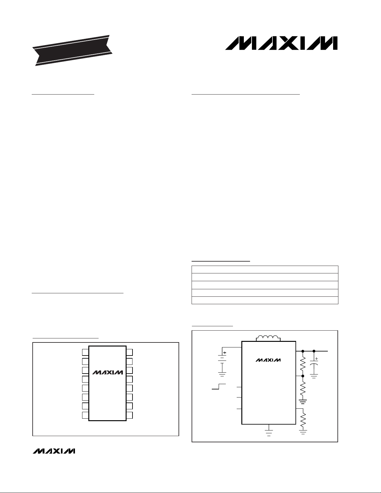
IN OUT
OUT
LX2
LX2
PGND
PGND
AGND
ON
TOP VIEW
MAX1687
MAX1688
TSSOP
IN
LX1
FB
LX1
LIM [CHG]
REF
N.C.
[ ] ARE FOR MAX1688
Typical Operating Circuit
19-1426; Rev 0; 2/99
PART*
MAX1687EUE
MAX1687ESA
MAX1688EUE
-40°C to +85°C
-40°C to +85°C
-40°C to +85°C
TEMP. RANGE PIN-PACKAGE
16 TSSOP
8 SO
16 TSSOP
Pin Configurations
Ordering Information
MAX1688ESA -40°C to +85°C
8 SO
Pin Configurations continued at end of data sheet.
†
Patent pending
*
U.S. and foreign patents pending.
EVALUATION KIT MANUAL
FOLLOWS DATA SHEET
2.7V TO 6V
1 Li-lon
OR
3 NiMH
OR
3 ALKALINE
ON
OFF
0 TO 1V
CONTROL INPUT
( ) ARE FOR MAX1687
[ ] ARE FOR MAX1688
LX1 LX2
IN
MAX1687
MAX1688
ON
(LIM)
REF
GND
OUT
FB
[CHG]
V
OUT
UP TO 6V

MAX1687/MAX1688
Step-Up DC-DC Converters with
Precise, Adaptive Current Limit for GSM
2 _______________________________________________________________________________________
ABSOLUTE MAXIMUM RATINGS
ELECTRICAL CHARACTERISTICS
(VIN= VON= +3V, V
LIM
= 1V (MAX1687), V
CHG
= 1V (MAX1688), VFB= 1.5V, V
OUT
= 6V, TA = 0°C to +85°C, unless otherwise noted.
Typical values are at T
A
= +25°C.)
Stresses beyond those listed under “Absolute Maximum Ratings” may cause permanent damage to the device. These are stress ratings only, and functional
operation of the device at these or any other conditions beyond those indicated in the operational sections of the specifications is not implied. Exposure to
absolute maximum rating conditions for extended periods may affect device reliability.
IN, ON, LX1, CHG, LIM, FB, OUT, REF to GND.......-0.3V to +7V
LX2 to GND ..............................................................-0.3V to +8V
IN, LX1 Average Current..........................................................1A
Continuous Power Dissipation (TA= +70°C)
TSSOP (derate 5.7mW/°C above +70°C) ....................457mW
SO (derate 5.88mW/°C above +70°C).........................471mW
Operating Temperature Range ...........................-40°C to +85°C
Storage Temperature Range .............................-65°C to +150°C
Lead Temperature (soldering, 10sec)............................+300° C
IN rising, 1% hysteresis
VFB= 0, V
OUT
= 3V (MAX1688)
VFB= 1.125V, V
OUT
= 3V (MAX1688)
VFBrising, 2% hysteresis
I
REF
= 0 to 10µA
VFB= 1.5V
Shutdown, VIN= 4.2V, LX2 connected to LX1,
V
OUT
= 0, ON = GND
V
LIM
= V
CHG
= 1V
CONDITIONS
0.744 0.8 0.856
Peak Current
VV
REF
6Output Voltage Range
V
2.4 2.5 2.6
V2.7 6Input Voltage Range
Input Undervoltage Lockout
µA60 110I
CHG
Source Current
mmho0.18 0.2 0.22g
mFB
FB Transconductance
V1.212 1.250 1.288FB Set Voltage
V1.225 1.25 1.275V
REF
Reference Voltage
mA
24
Input Supply Current
µA310
UNITSMIN TYP MAXSYMBOLPARAMETER
V
LIM
= V
CHG
= 1V
V
LIM
= V
CHG
= 0.65V
VIN= 2.7V
V
LIM
= 1V
VON= 0 or 3V
VIN= 2.7V
VIN= 6V
VIN= 4.2V
VFB= 1.5V
VIN= 2.7V Ω0.3 0.7P-Channel On-Resistance
Ω0.1 0.18R
SENSE
Sense Resistor
mA170 200 230I
RIPPLE
A
0.46 0.5 0.54
I
PEAK
Ripple Current
Ω0.4 0.8N-Channel On-Resistance
2
0.02 0.1
I
LIM
0.02 0.1I
ON
V0.6V
IL
V
1.8
ON Input Low Voltage
1.5
0.05 0.2I
FB
Input Current
VIN= V
LX2
= 6V, V
OUT
= VON= 0
VIN= 4V, V
FB
= 0, V
OUT
= 0
µA0.05 10
Ω30 70Precharge On-Resistance
LX2 Leakage Current
ms0.7 1.2 1.8t
DELAY
Shutdown Delay
V
IH
ON Input High Voltage
µA
TA= 0°C to +85°C
TA= +25°C

MAX1687/MAX1688
Step-Up DC-DC Converters with
Precise, Adaptive Current Limit for GSM
_______________________________________________________________________________________ 3
ELECTRICAL CHARACTERISTICS
(VIN= VON= +3V, V
LIM
= 1V (MAX1687), V
CHG
= 1V (MAX1688), VFB= 1.5V, V
OUT
= 6V, TA= -40°C to +85°C, unless otherwise noted.)
(Note 1)
Note 1: Specifications to -40°C are guaranteed by design, not production tested.
V
LIM
= V
CHG
= 1V
V
LIM
= V
CHG
= 0.65V
I
IN
IN rising, 1% hysteresis
VFB= 1.125V, V
OUT
= 3V (MAX1688)
FB rising, 2% hysteresis
I
REF
= 0 to 10µA
VFB= 1.5V
Shutdown VIN= 4.2V, LX2 connected to LX1,
V
OUT
= 0, ON = GND
V
LIM
= V
CHG
= 1V
CONDITIONS
mA
145 240
I
RIPPLE
Ripple Current
A
0.44 0.57
I
PEAK
Ω
0.18
R
SENSE
Sense Resistor
0.73 0.90
Peak Current
V
2.35 2.65
V
2.7 6
Input Voltage Range
Input Undervoltage Lockout
mmho
0.16 0.24
gm
FB
FB Transconductance
V
1.20 1.30
FB Set Voltage
V1.212 1.288V
REF
Reference Voltage
ms
0.6 2
T
DELAY
Shutdown Delay
mA
5
I
SHDN
Input Supply Current
µA10
UNITSMIN TYP MAXSYMBOLPARAMETER
VIN= 4V, V
FB
= 0, V
OUT
= 0
VIN= 2.7V
VIN= 2.7V
Ω
70
Precharge On-Resistance
Ω
0.7
Ω
0.8
N-Channel On-Resistance
P-Channel On-Resistance
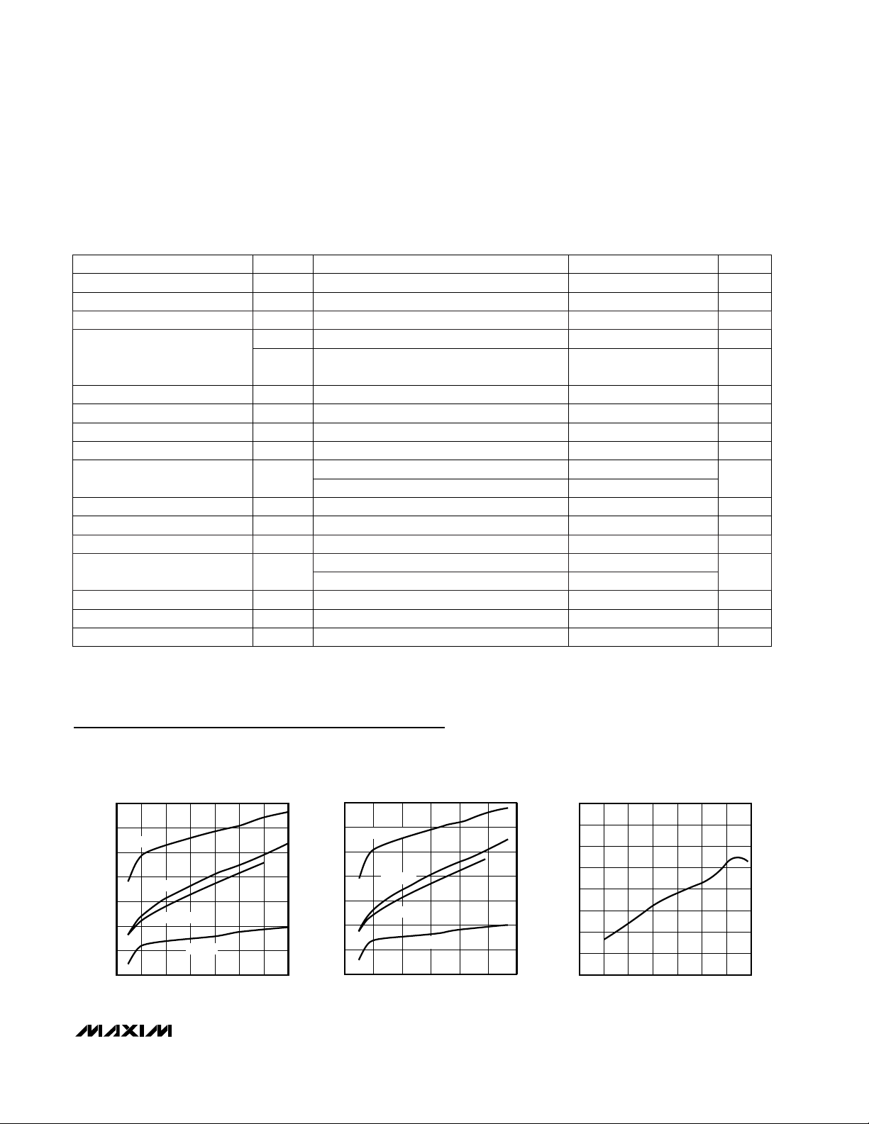
Typical Operating Characteristics
(VIN= +3.3V, V
OUT
= 5V, V
LIM
= 1V, Figures 6b and 7, TA= +25°C, unless otherwise noted.)
60
70
65
80
75
85
95
90
0 150 20050 100 250 300 350
EFFICIENCY vs. DC LOAD CURRENT
(V
OUT
= 5.5V)
MAX1687/88 toc01
LOAD CURRENT (mA)
EFFICIENCY (%)
VIN = 5V
VIN = 3.3V
VIN = 2.7V
VIN = 6V
60
65
70
75
80
85
90
95
0 1500500 1000 2000 2500 3000
EFFICIENCY vs. GSM BURST LOAD
(V
OUT
= 5.5V)
MAX1687/88 toc02
LOAD CURRENT (mA)
EFFICIENCY (%)
VIN = 5V
VIN = 3.3V
VIN = 2.7V
VIN = 6V
60
70
65
80
75
95
90
85
100
0 10050 150 200 250 300 350
EFFICIENCY vs. LOAD CURRENT
(V
IN
= 2.7V, V
OUT
= 3.3V)
MAX1687/88 toc03
LOAD CURRENT (mA)
EFFICIENCY (%)
VIN= 2.7V V
0.6
V
IL
ON Input Low Voltage
V
VIN= 6V
VIN= 4.2V
V
IH
ON Input High Voltage
1.8
1.5
V
V
REF
6
Output Voltage Range

MAX1687/MAX1688
Step-Up DC-DC Converters with Precise,
Adaptive Current Limit for GSM
4 _______________________________________________________________________________________
_____________________________
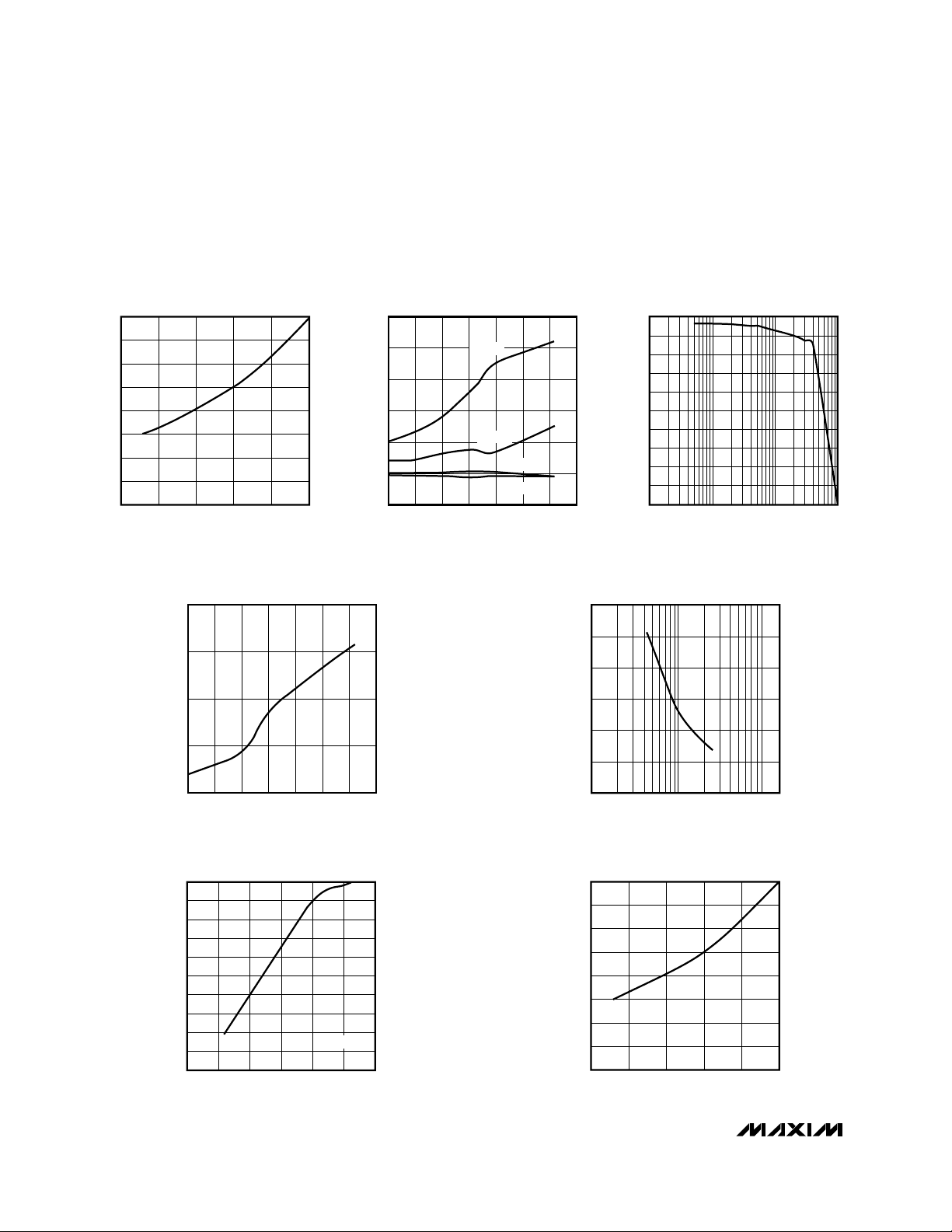
Typical Operating Characteristics (continued)
(V
IN
= +3.3V, V
OUT
= 5V, V
LIM
= 1V, Figures 6b and 7, TA= +25°C, unless otherwise noted.)
300
450
400
350
500
550
600
650
700
750
800
100 200150 250 300 350 400
MAX1688
I
PEAK
vs. V
OUT
DROOP
MAX1687/88 toc09
V
OUT
DROOP (mV)
I
PEAK
(mA)
R
CHG
= 40.2k
0
800
700
600
500
400
300
200
100
15 20 25 30 35 40
MAX1688 PEAK INDUCTOR CURRENT
vs. R
CHG
(1A GSM LOAD)
MAX1687/88 toc10
R
CHG
(kΩ)
PEAK INDUCTOR CURRENT (mA)
0
100
200
300
400
500
600
700
800
15 20 25 30 35 40
MAX1688 PEAK BATTERY CURRENT
vs. R
CHG
(1A GSM LOAD)
MAX1687/88 toc04
R
CHG
(kΩ)
PEAK BATTERY CURRENT (mA)
1.5
2.5
2.0
3.5
3.0
4.0
4.5
-40 20 40-20 0 60 80 100
TEMPERATURE (°C)
SUPPLY CURRENT (mA)
NO-LOAD BATTERY INPUT CURRENT vs.
TEMPERATURE (V
OUT
= 5V, V
LIM
= 1V )
MAX1687/88 toc05
VIN = 5V
VIN = 3.3V
VIN = 2.7V
VIN = 6V
REFERENCE VOLTAGE vs. REFERENCE
CURRENT (V
IN
= 3.3V, V
OUT
= 5V)
MAX1687/88 toc06
I
REF
(µA)
V
REF
(V)
1.245
1.200
1 100010010
1.215
1.205
1.235
1.225
1.250
1.220
1.210
1.240
1.230
1.245
1.247
1.249
1.251
1.253
TEMPERATURE (°C)
REFERENCE VOLTAGE (V)
-40 20 40-20 0 60 80 100
REFERENCE VOLTAGE vs. TEMPERATURE
(V
IN
= 3.3V, V
OUT
= 5V)
MAX1687/88 toc07
1200
0
1 10 100
SWITCHING FREQUENCY vs. INDUCTANCE
(V
IN
= 3.3V, V
OUT
= 5V,
I
LOAD
= 100mA, V
LIM
= 1V)
200
MAX1687/88 toc08
INDUCTANCE (µH)
FREQUENCY (kHz)
600
400
1000
800
 Loading...