For free samples & the latest literature: http://www.maxim-ic.com, or phone 1-800-998-8800.
For small orders, phone 1-800-835-8769.
General Description
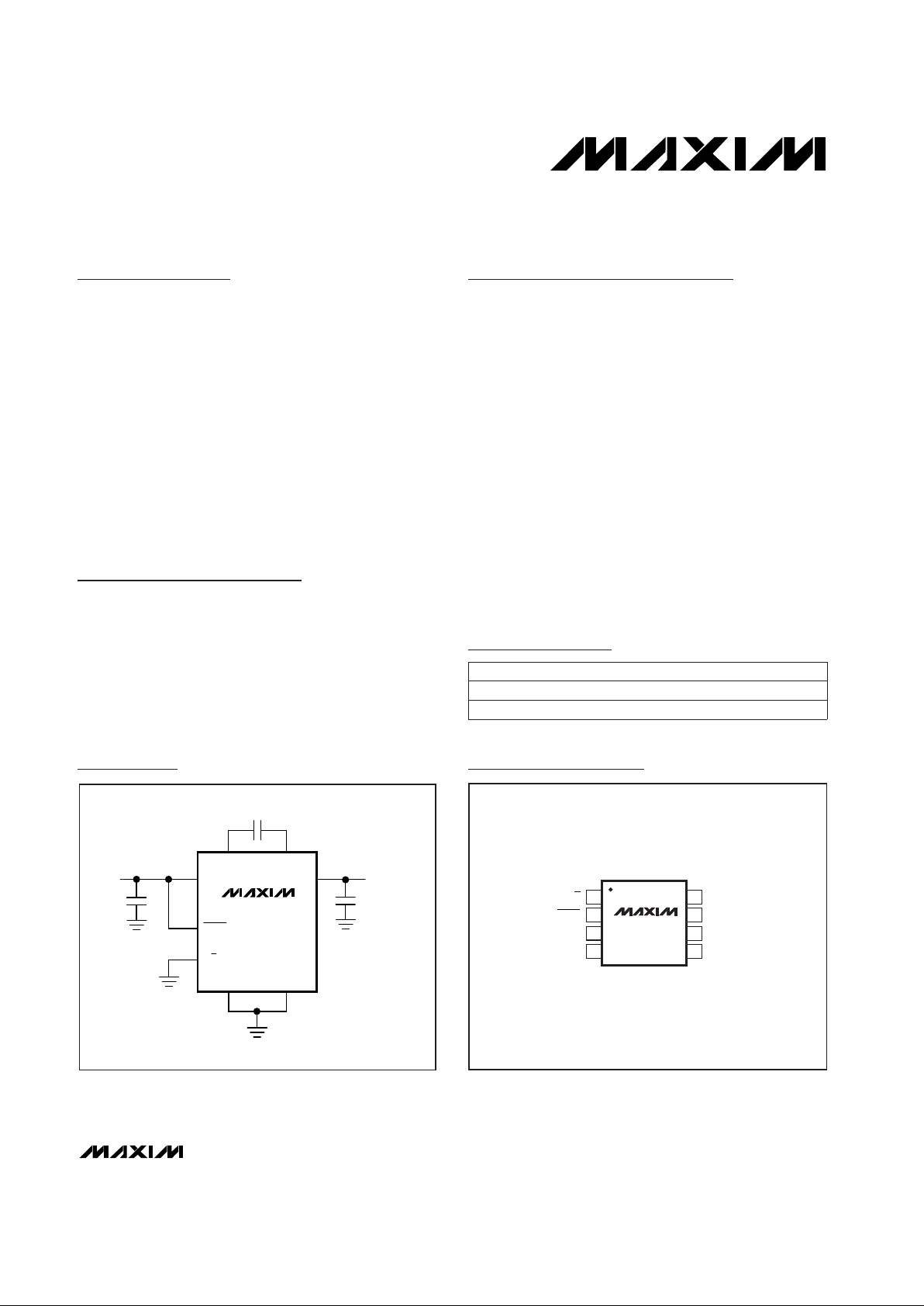
The MAX1686 provides power for dual-voltage subscriber ID module (SIM) cards in portable applications
such as GSM cellular phones. Designed to reside in the
portable unit (cellular phone handset), the 1MHz charge
pump converts a 2.7V to 4.2V input to regulated 5V output. The MAX1686H has a nominal output voltage of
5.0V, while the MAX1686 is set to 4.75V to reduce SIMcard current drain. The charge pump has only 45µA quiescent supply current, which reduces to 3µA when a
3V-capable SIM card is being powered and the charge
pump is disabled. An internal input/output shorting
switch provides power for 3V SIM cards.
The MAX1686/MAX1686H require only three external
capacitors around their space-saving, thin (1mm) 8-pin
µMAX packages.
Applications
GSM Cellular Phones
PCS Phones
Portable POS Terminals
Personal Communicators
Features
♦ 2.7V to 4.2V Input Range
♦ 12mA min Charge-Pump Output Current
♦ 45µA Quiescent Supply Current
♦ 0.1µA Supply Current in Shutdown Mode
♦ 5.0V Regulated Charge-Pump Output (MAX1686H)
4.75V Regulated Charge-Pump Output (MAX1686)
♦ Input-Output Shorting Switch for 3V Cards
♦ Small External Components
(Uses a 0.047µF, 0.1µF, and a 2.2µF Capacitor)
♦ Output Driven to Ground in Shutdown Mode
♦ Super-Small 8-Pin µMAX Package
♦ Soft-Start and Short-Circuit Protection
MAX1686/MAX1686H
3V to 5V Regulating
Charge Pumps for SIM Cards
________________________________________________________________
Maxim Integrated Products
1
1
2
3
4
8
7
6
5
OUT
CXP
CXN
PGNDGND
IN
SHDN
3/5
MAX1686
MAX1686H
µMAX
TOP VIEW
MAX1686
MAX1686H
IN
CXN CXP
GND PGND
C
IN
INPUT
2.7V TO 4.2V
OUTPUT
V
IN
OR 5V/20mA
C
X
C
OUT
SHDN
3/5
OUT
Typical Operating Circuit
19-1376; Rev 1; 12/98
PART
MAX1686EUA
-40°C to +85°C
TEMP. RANGE PIN-PACKAGE
8 µMAX
Pin Configuration
Ordering Information
MAX1686HEUA
-40°C to +85°C 8 µMAX

MAX1686/MAX1686H
3V to 5V Regulating
Charge Pumps for SIM Cards
2 _______________________________________________________________________________________
ABSOLUTE MAXIMUM RATINGS
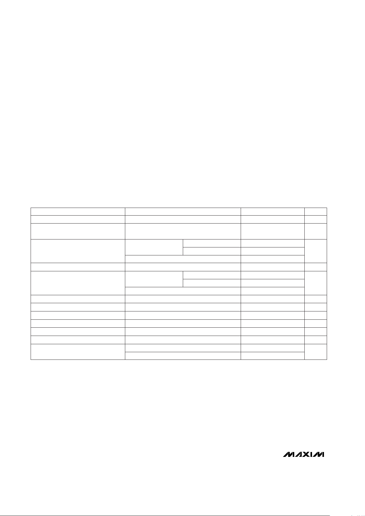
ELECTRICAL CHARACTERISTICS
(VIN= V
SHDN
= 3.3V, 3/5 = GND, CX= 0.22µF, C
OUT
= 10µF (see
Applications Information
section to use smaller capacitors),
T
A
= T
MIN
to T
MAX
, unless otherwise noted. Typical values are at TA= +25°C.) (Note 1)
IN, OUT, SHDN, 3/5 to GND.....................................-0.3V to +6V
CXP to GND..............................................-0.3V to (V
OUT
+ 0.3V)
CXN to GND ................................................-0.3V to (V
IN
+ 0.3V)
PGND to GND ......................................................-0.3V to + 0.3V
OUT Short Circuit to GND..........................................Continuous
IN-to-OUT Current...............................................................50mA
Continuous Power Dissipation (T
A
= +70°C )
8-Pin µMAX (derate 4.1mW/°C above +70°C).............330mW
Operating Temperature Range
MAX1686EUA/MAX1686HEUA........................-40°C to +85°C
Junction Temperature......................................................+150°C
Storage Temperature Range.............................-65°C to +165°C
Lead Temperature (soldering, 10sec).............................+300°C
PARAMETER
CONDITIONS MIN TYP MAX UNITS
Input Voltage Range 2.7 4.2 V
Input Undervoltage-Lockout
Threshold Voltage
0.8 1.2 1.6 V
Quiescent Supply Current
Charge pump enabled,
no load, 3/5 = GND
µA
Charge pump disabled, no load, 3/5 = IN
Shutdown Supply Current
V
IN
= 3.6V, SHDN = GND
0.1 5
VOUT Output Voltage
4.55 4.75 5.25
V
3/5
= VIN= 3.0V 2.5 5 Ω
OUT Short-Circuit Current
3/5 = GND or IN
20 100 200 mA
Logic Input Low Voltage
SHDN, 3/5
0.5 · VIN0.3 · V
IN
V
Logic Input High Voltage
SHDN, 3/5
0.7 · VIN0.5 · V
IN
V
Logic Input Leakage Current
SHDN, 3/5 = GND or IN
0.1 1 µA
4.75 5.00 5.25
OUT Discharge Switch On-Resistance
3/5 = GND or IN, SHDN = GND
80 200 Ω
IN-to-OUT Switch On-Resistance
TA= +25°C 800 1000 1200
µA
Note 1: Electrical specifications are measured by pulse testing and are guaranteed for a junction temperature within the operating
temperature range, unless otherwise noted. Limits are 100% production tested at T
A
= +25°C. Limits over the entire operating temperature range are guaranteed through correlation using Statistical Quality Control (SQC) methods and are not production tested.
Stresses beyond those listed under “Absolute Maximum Ratings” may cause permanent damage to the device. These are stress ratings only, and functional
operation of the device at these or any other conditions beyond those indicated in the operational sections of the specifications is not implied. Exposure to
absolute maximum rating conditions for extended periods may affect device reliability.
TA= +25°C 45 100
310
Charge-Pump Frequency
TA= -40°C to +85°C 700 1300
kHz
TA= -40°C to +85°C 150
3/5 = IN
V
IN
MAX1686
MAX1686H
VIN= 2.7V to 4.2V,
load = 0 to 12mA

MAX1686/MAX1686H
3V to 5V Regulating
Charge Pumps for SIM Cards
_______________________________________________________________________________________
3
0
0.1 100101
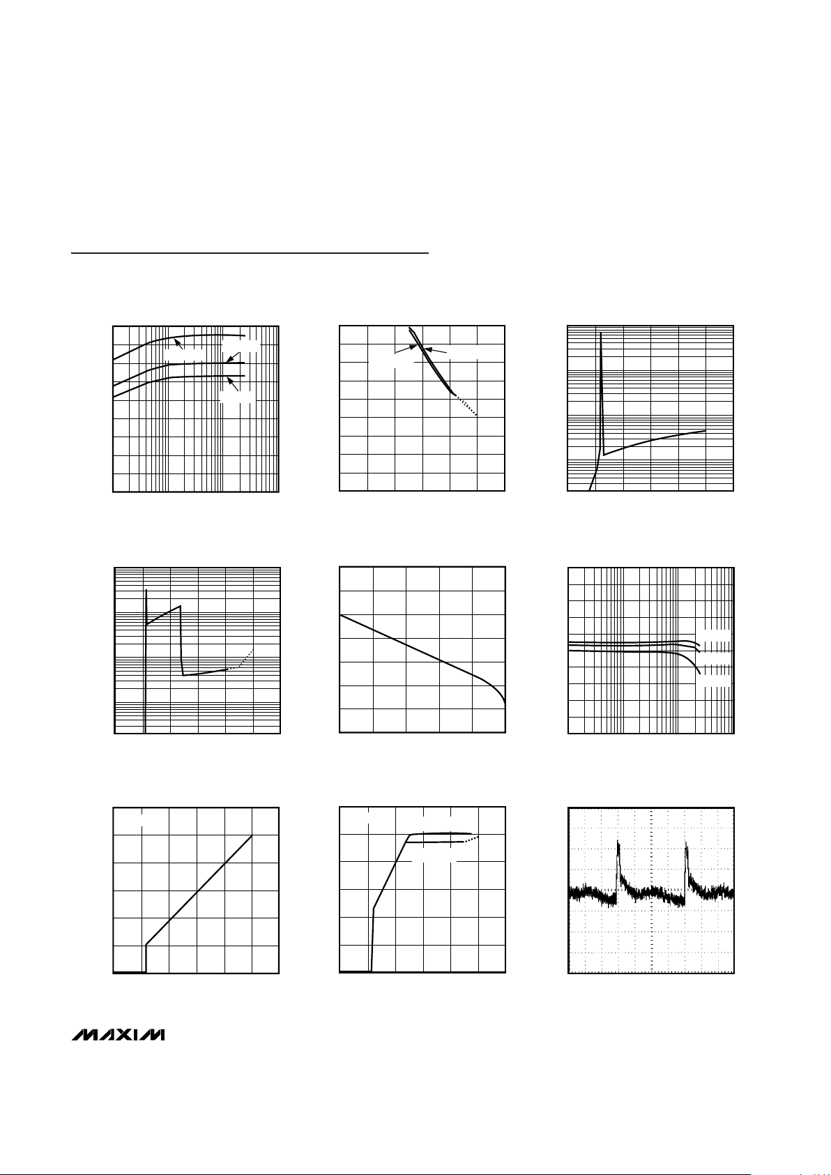
EFFICIENCY vs. LOAD CURRENT
(5V MODE)
30
10
70
50
90
40
20
80
60
MAX1686-01
LOAD CURRENT (mA)
EFFICIENCY (%)
V
IN
= 3.6V
V
IN
= 2 .7V
V
IN
= 3.3V
0
0
EFFICIENCY vs. INPUT VOLTAGE
(5V MODE)
MAX1686-TOC2
INPUT VOLTAGE (V)
EFFICIENCY (%)
10
20
30
40
50
60
70
80
90
123 456
I
LOAD
= 10mA
I
LOAD
= 1mA
1000
0.1
02146
NO-LOAD INPUT CURRENT
vs. INPUT VOLTAGE (3V MODE)
1
10
100
MAX1686-03
INPUT VOLTAGE (V)
INPUT CURRENT (µA)
35
10,000
1
02146
NO-LOAD INPUT CURRENT
vs. INPUT VOLTAGE (5V MODE)
10
100
1000
MAX1686-04
INPUT VOLTAGE (V)
INPUT CURRENT (µA)
35
0
2
1
4
3
5
6
0231 456
OUTPUT VOLTAGE
vs. INPUT VOLTAGE (3V MODE)
MAX1686-07
INPUT VOLTAGE (V)
OUTPUT VOLTAGE (V)
NO LOAD
3.20
3.24
3.22
3.28
3.26
3.30
3.34
3.32
0 5 10 15 20 25
OUTPUT VOLTAGE
vs. LOAD CURRENT (3V MODE)
MAX1686-05
LOAD CURRENT (mA)
OUTPUT VOLTAGE (V)
4.70
0.1 100101
MAX1686 OUTPUT VOLTAGE
vs. LOAD CURRENT (5V MODE)
4.73
4.71
4.77
4.75
4.80
4.74
4.72
4.78
4.79
4.76
MAX1686-06
LOAD CURRENT (mA)
OUTPUT VOLTAGE (V)
V
IN
= 2.7V
V
IN
= 3 .3V
V
IN
= 3.6V
0
2
1
4
3
5
6
0231 456
OUTPUT VOLTAGE
vs. INPUT VOLTAGE (5V MODE)
MAX1686-08
INPUT VOLTAGE (V)
OUTPUT VOLTAGE (V)
NO LOAD
MAX1686
MAX1686H
2.5µs/div
OUTPUT WAVEFORM
(I
LOAD
= 10mA)
MAX1686-09
V
OUT
(20mV/div)
5V MODE, AC COUPLED,
C
OUT
= 10µF 0.1µF
Typical Operating Characteristics
(See
Typical Operating Circuit
, CIN= 0.47µF, CX= 0.22µF, C
OUT
= 10µF, VIN= 3.3V, TA= +25°C, unless otherwise noted.)
 Loading...