

Page 1
For free samples & the latest literature: http://www.maxim-ic.com, or phone 1-800-998-8800.
For small orders, phone 408-737-7600 ext. 3468.
General Description
The ultra-small MAX1682/MAX1683 monolithic, CMOS
charge-pump voltage doublers accept input voltages
ranging from +2.0V to +5.5V. Their high voltage-conversion efficiency (over 98%) and low operating current
(110µA for MAX1682) make these devices ideal for
both battery-powered and board-level voltage-doubler
applications.
Oscillator control circuitry and four power MOSFET
switches are included on-chip. The MAX1682 operates
at 12kHz and the MAX1683 operates at 35kHz. A typical application includes generating a 6V supply to
power an LCD display in a hand-held PDA. Both parts
are available in a 5-pin SOT23 package and can deliver
30mA with a typical voltage drop of 600mV.
________________________Applications
Small LCD Panels
Cell Phones
Handy-Terminals
PDAs
____________________________Features
♦ 5-Pin SOT23 Package
♦ +2.0V to +5.5V Input Voltage Range
♦ 98% Voltage-Conversion Efficiency
♦ 110µA Quiescent Current (MAX1682)
♦ Requires Only Two Capacitors
♦ Up to 45mA Output Current
MAX1682/MAX1683
Switched-Capacitor Voltage Doublers
________________________________________________________________
Maxim Integrated Products
1
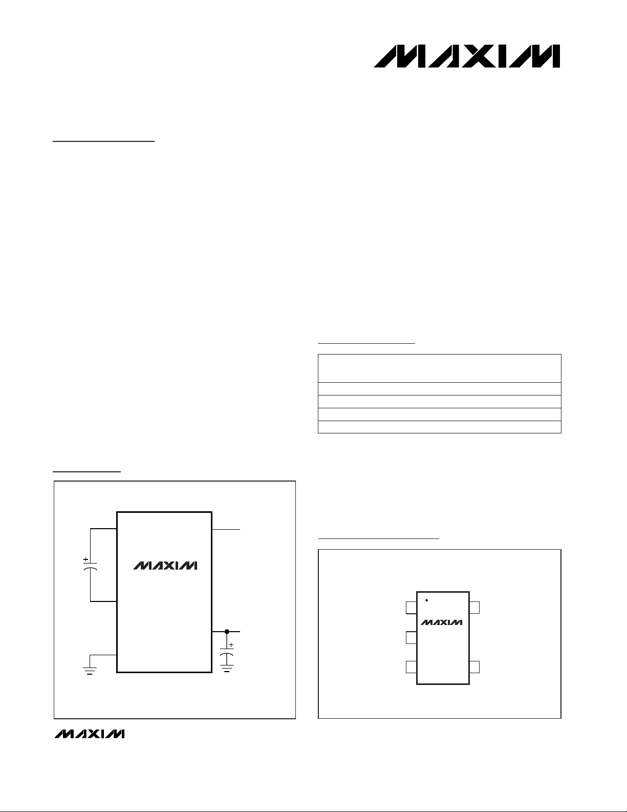
OUT
INC1-
15C1+GND
MAX1682
MAX1683
SOT23-5
TOP VIEW
2
34
Pin Configuration
VOLTAGE DOUBLER
C1+
C1-
IN
OUT
GND
INPUT
SUPPLY
VOLTAGE
OUTPUT
VOLTAGE
2 x V
IN
MAX1682
MAX1683
1
3
C1
C2
54
2
V
IN
Typical Operating Circuit
19-1305; Rev 1; 8/98
PART
MAX1682C/D
MAX1682EUK-T
MAX1683C/D
0°C to +70°C
-40°C to +85°C
0°C to +70°C
TEMP.
RANGE
PIN-
PACKAGE
Dice*
5 SOT23-5
Dice*
Ordering Information
Note: These parts are available in tape-and-reel only. Minimum
order quantity is 2500 pieces.
*
Dice are tested at TA= +25°C.
MAX1683EUK-T -40°C to +85°C 5 SOT23-5
SOT
TOP MARK
—
ACLL
—
ACCM
Page 2
MAX1682/MAX1683
Switched-Capacitor Voltage Doublers
2 _______________________________________________________________________________________
ABSOLUTE MAXIMUM RATINGS
ELECTRICAL CHARACTERISTICS
(VIN= +5.0V, capacitor values from Table 2, TA= 0°C to +85°C, unless otherwise noted. Typical values are at TA= +25°C.)
ELECTRICAL CHARACTERISTICS
(VIN= +5.0V, capacitor values from Table 2, TA= -40°C to +85°C, unless otherwise noted.) (Note 3)
Stresses beyond those listed under “Absolute Maximum Ratings” may cause permanent damage to the device. These are stress ratings only, and functional
operation of the device at these or any other conditions beyond those indicated in the operational sections of the specifications is not implied. Exposure to
absolute maximum rating conditions for extended periods may affect device reliability.
Note 2: Once started, the MAX1682/MAX1683 typically operate down to 1V.
Note 3: Specifications at -40°C to +85°C are guaranteed by design.
IN to GND.................................................................+6V to -0.3V
OUT to GND.......................................................+12V, V
IN
- 0.3V
OUT Output Current............................................................50mA
Output Short-Circuit Duration.................................1sec (Note 1)
Continuous Power Dissipation (T
A
= +70°C)
SOT23-5 (derate 7.1mW/°C above +70°C)...................571mW
Operating Temperature Range
MAX1682EUK/MAX1683EUK ...........................-40°C to +85°C
Junction Temperature......................................................+150°C
Storage Temperature Range.............................-65°C to +160°C
Lead Temperature (soldering, 10sec).............................+300°C
(Note 2)
TA= +25°C
TA= +25°C
I
OUT
= 0mA, TA= +25°C
CONDITIONS
V1Minimum Operating Voltage
µA
230 310
110 145
No-Load Supply Current
8.4 12 15.6
kHz
24.5 35 45.5
Oscillator Frequency
%98 99.9Voltage Conversion Efficiency
UNITSMIN TYP MAXPARAMETER
Note 1: Avoid shorting OUT to GND, as it may damage the device. For temperatures above +85°C, shorting OUT to GND even
instantaneously will damage the device.
MAX1682
MAX1683
R
LOAD
= 10kΩ
TA= +25°C
TA= 0°C to +85°C
V
2.1 1.8 5.5
2.0 1.7 5.5
Supply Voltage Range
MAX1682
MAX1683
TA= +25°C
TA= 0°C to +85°C
I
OUT
= 5mA
20 50
Ω
65
Output Resistance
I
OUT
= 0mA
I
OUT
= 5mA
MAX1683
MAX1682
R
LOAD
= 10kΩ
MAX1683
MAX1682
CONDITIONS
%97Voltage Conversion Efficiency
Ω65Output Resistance
kHz
17.5 57.8
Oscillator Frequency
6.6 18.6
V2.3 5.5Supply-Voltage Range
µA
350
160
No-Load Supply Current
UNITSMIN TYP MAXPARAMETER
Page 3
MAX1682/MAX1683
Switched-Capacitor Voltage Doublers
_______________________________________________________________________________________
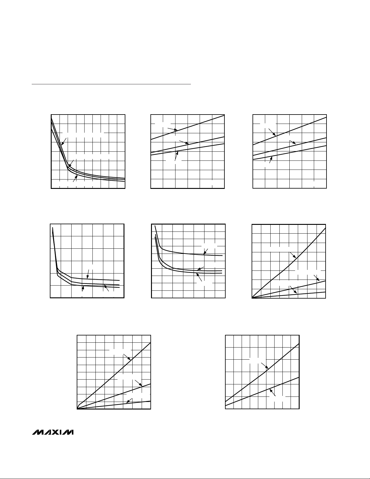
3
10
30
20
60
50
40
80
70
90
1.0 2.5 3.01.5 2.0 3.5 4.0 4.5 5.0 5.5
OUTPUT RESISTANCE
vs. SUPPLY VOLTAGE
MAX1682/83 TOC1
VIN (V)
OUTPUT RESISTANCE (Ω)
MAX1683, C1 = C2 = 3.3µF
MAX1683, C1 = C2 = 10µF
MAX1682, C1 = C2 = 10µF
0
5
10
15
20
25
30
35
40
-40 0-20 20 40 60 80
MAX1682 OUTPUT RESISTANCE
vs. TEMPERATURE
MAX1682/83 TOC02
TEMPERATURE (°C)
OUTPUT RESISTANCE (Ω)
I
LOAD
= 5mA
VIN = 5V
VIN = 3.3V
VIN = 2V
0
5
10
15
20
25
30
35
40
-40 0-20 20 40 60 80
MAX1683 OUTPUT RESISTANCE
vs. TEMPERATURE
MAX1682/83 TOC03
TEMPERATURE (°C)
OUTPUT RESISTANCE (Ω)
I
LOAD
= 5mA
VIN = 5V
VIN = 3.3V
VIN = 2V
0
40
20
80
60
100
120
0 15 205 10 25 30 35
MAX1682 OUTPUT RESISTANCE
vs. CAPACITANCE
MAX1682/83 TOC4
CAPACITANCE (µF)
OUTPUT RESISTANCE (Ω)
VIN = 5V
VIN = 3.3V
VIN = 2V
0
200
100
400
300
600
500
700
900
800
1000
0 10 155 20 25 30 35 40
MAX1683
OUTPUT VOLTAGE RIPPLE
vs. OUTPUT CURRENT
MAX1682/83 TOC07
I
OUT
(mA)
V
RIPPLE
(mV)
C1 = C2 =1µF
C1 = C2 = 3.3µF
C1 = C2 = 10µF
0
15
10
5
25
20
45
40
35
30
50
0 5 10 15 20 25 30 35
MAX1683 OUTPUT RESISTANCE
vs. CAPITANCE
MAX1682/83 TOC05
CAPACITANCE (µF)
OUTPUT RESISTANCE (Ω)
VIN = 2V
VIN = 3.3V
VIN = 5V
0
200
100
400
300
500
600
700
800
0 10 155 20 25 30 35 40
MAX1682
OUTPUT VOLTAGE RIPPLE
vs. OUTPUT CURRENT
MAX1682/83 TOC06
I
OUT
(mA)
V
RIPPLE
(mV)
C1 = C2 = 3.3µF
C1 = C2 = 10µF
C1 = C2 = 33µF
0
50
100
150
200
250
300
1.0 2.01.5 2.5 3.0 3.5 4.0 4.5 5.0 5.5
SUPPLY CURRENT
vs. SUPPLY VOLTAGE
MAX1682/83 TOC09
SUPPLY VOLTAGE (V)
SUPPLY CURRENT (µA)
MAX1683
MAX1682
Typical Operating Characteristics
(Typical Operating Circuit, VIN= +5V, C1 = C2 = 10µF for the MAX1682 and 3.3µF for the MAX1683, TA= +25°C, unless otherwise
noted.)
Page 4

MAX1682/MAX1683
Switched-Capacitor Voltage Doublers
4 _______________________________________________________________________________________
Typical Operating Characteristics (continued)
(Typical Operating Circuit, VIN= +5V, C1 = C2 = 10µF for the MAX1682 and 3.3µF for the MAX1683, TA= +25°C, unless otherwise
noted.)
11.0
11.5
12.0
12.5
-40 0 20-20 40 60 80
MAX1682 OSCILLATOR FREQUENCY
vs. TEMPERATURE
MAX1682/83 TOC10
TEMPERATURE (°C)
OSCILLATOR FREQUENCY (kHz)
VIN = 5V
VIN = 3.3V
VIN = 2V
28
32
30
36
34
38
40
-40 0 20-20 40 60 80
MAX1683 OSCILLATOR FREQUENCY
vs. TEMPERATURE
MAX1682/83 TOC11
TEMPERATURE (°C)
OSCILLATOR FREQUENCY (kHz)
VIN = 5V
VIN = 3.3V
VIN = 2V
0
2
1
4
3
6
5
7
9
8
10
0 10 15 205 25 30 35 4540 50
MAX1682 OUTPUT VOLTAGE
vs. OUTPUT CURRENT
MAX1682/83 TOC12
OUTPUT CURRENT (mA)
OUTPUT VOLTAGE (V)
VIN = 5V
VIN = 3.3V
VIN = 2V
0
2
1
4
3
6
5
7
9
8
10
0 10 15 205 25 30 35 4540 50
MAX1683 OUTPUT VOLTAGE
vs. OUTPUT CURRENT
MAX1682/83 TOC13
OUTPUT CURRENT (mA)
OUTPUT VOLTAGE (V)
VIN = 5V
VIN = 3.3V
VIN = 2V
20µs/div
V
OUT
20mV/div
I
LOAD
= 5mA, VIN = 5V, C1 = C2 = 10µF
MAX1682
OUTPUT RIPPLE
MAX1682toc16
80
86
84
82
88
90
92
94
96
98
100
0 105 15 20 25 30
MAX1682 EFFICIENCY vs.
LOAD CURRENT
MAX1682/83 TOC14
LOAD CURRENT (mA)
EFFICIENCY (%)
VIN = 5V
VIN = 3.3V
VIN = 2V
80
86
84
82
88
90
92
94
96
98
100
0 105 15 20 25 30
MAX1683 EFFICIENCY vs.
LOAD CURRENT
MAX1682/83 TOC15
LOAD CURRENT (mA)
EFFICIENCY (%)
VIN = 5V
VIN = 3.3V
VIN = 2V
MAX1683
OUTPUT RIPPLE
MAX1682toc17
I
LOAD
= 5mA, VIN = 5V, C1 = 3.3µF, C2 = 10µF
20µs/div
V
OUT
20mV/div
0
0.5
1.0
1.5
2.0
2.5
700 30 10100 70300 7 3 1 0.7 0.3
START-UP VOLTAGE
vs. RESISTIVE LOAD
MAX1682toc18
R
LOAD
(kΩ)
V
START
(V)
MAX1682
MAX1683
Page 5

_______________Detailed Description
The MAX1682/MAX1683 capacitive charge pumps
double the voltage applied to their input. Figure 1
shows a simplified functional diagram of an ideal voltage doubler. During the first half-cycle, switches S1
and S2 close, and capacitor C1 charges to VIN. During
the second half cycle, S1 and S2 open, S3 and S4
close, and C1 is level shifted upward by VINvolts. This
connects C1 to the reservoir capacitor C2, allowing
energy to be delivered to the output as necessary. The
actual voltage is slightly lower than 2 x VIN, since
switches S1–S4 have resistance and the load drains
charge from C2.
Charge-Pump Output
The MAX1682/MAX1683 have a finite output resistance
of about 20Ω (Table 2). As the load current increases,
the devices’ output voltage (V
OUT
) droops. The droop
equals the current drawn from V
OUT
times the circuit’s
output impedance (RS), as follows:
V
DROOP
= I
OUT
x R
S
V
OUT
= 2 x VIN- V
DROOP
Efficiency Considerations
The power efficiency of a switched-capacitor voltage
converter is affected by three factors: the internal losses
in the converter IC, the resistive losses of the capacitors,
and the conversion losses during charge transfer
between the capacitors. The total power loss is:
The internal losses are associated with the IC’s internal
functions, such as driving the switches, oscillator, etc.
These losses are affected by operating conditions such
as input voltage, temperature, and frequency.
The next two losses are associated with the voltage
converter circuit’s output resistance. Switch losses
occur because of the on-resistance of the MOSFET
switches in the IC. Charge-pump capacitor losses
occur because of their ESR. The relationship between
these losses and the output resistance is as follows:
where f
OSC
is the oscillator frequency. The first term is
the effective resistance from an ideal switchedcapacitor circuit (Figures 2a and 2b).
P P
I x R
R
f x C
R ESR
ESR
PUMP CAPACITOR LOSSES SWITCH LOSSES
OUT OUT
OUT
OSC
SWITCHES C
C
+ =
≅
( )
+ +
+
2
1
2
1
1
2 4
ΣP P
P
P
LOSS INTERNAL LOSSES
PUMP CAPACITOR LOSSES
CONVERSION LOSSES
=
+
+
MAX1682/MAX1683
Switched-Capacitor Voltage Doublers
_______________________________________________________________________________________ 5
_____________________Pin Description
NAME FUNCTION
1 GND Ground
2 OUT
Doubled Output Voltage. Connect C2
between OUT and GND.
PIN
3 C1-
Negative Terminal of the Flying
Capacitor
4 IN Input Supply
5 C1+
Positive Terminal of the Flying
Capacitor
Figure 2a. Switched-Capacitor Model
V+
C1
f
C2 R
L
V
OUT
Figure 1. Simplified Functional Diagram of Ideal Voltage
Doubler
S1
V
IN
S3
S2
V
IN
V
OUT
S4
C1
C2
Figure 2b. Equivalent Circuit
R
EQUIV
=
R
EQUIV
V
OUT
R
L
1
V+
f × C1
C2
Page 6

MAX1682/MAX1683
Conversion losses occur during the charge transfer
between C1 and C2 when there is a voltage difference
between them. The power loss is:
where V
RIPPLE
is the peak-to-peak output voltage ripple
determined by the output capacitor and load current
(see
Output Capacitor
section). Choose capacitor val-
ues that decrease the output resistance (see
Flying
Capacitor
section).
Applications Information
Flying Capacitor (C1)
To maintain the lowest output resistance, use capacitors with low ESR. Suitable capacitor manufacturers are
listed in Table 1. The charge-pump output resistance is
a function of C1 and C2’s ESR and the internal switch
resistance, as shown in the equation for R
OUT
in the
Efficiency Considerations
section.
Minimizing the charge-pump capacitor’s ESR minimizes the total resistance. Suggested values are listed
in Tables 2 and 3.
Using a larger flying capacitor reduces the output
impedance and improves efficiency (see the
Efficiency
Considerations
section). Above a certain point, increasing C1’s capacitance has a negligible effect because
the output resistance becomes dominated by the internal switch resistance and capacitor ESR (see the
Output Resistance vs. Capacitance graph in the
Typical Operating Characteristics
). Table 2 lists the
most desirable capacitor values—those that produce a
low output resistance. But when space is a constraint, it
may be necessary to sacrifice low output resistance for
the sake of small capacitor size. Table 3 demonstrates
how the capacitor affects output resistance.
Output Capacitor (C2)
Increasing the output capacitance reduces the output
ripple voltage. Decreasing its ESR reduces both output
resistance and ripple. Smaller capacitance values can
be used with light loads. Use the following equation to
calculate the peak-to-peak ripple:
V
RIPPLE
= I
OUT
/ (f
OSC
x C2) + 2 x I
OUT
x ESR
C2
Input Bypass Capacitor
Bypass the incoming supply to reduce its AC impedance and the impact of the MAX1682/MAX1683’s
switching noise. When loaded, the circuit draws a continuous current of 2 x I
OUT
. A 0.1µF bypass capacitor is
sufficient.
P / C1 4V V
/ C2 2V V V x f
CONVERSION LOSS
1
2 IN
2
OUT
2
1
2 OUT RIPPLE
2
RIPPLE
OSC
= −
+
−
Switched-Capacitor Voltage Doublers
6 _______________________________________________________________________________________
Table 1. Recommended Capacitor Manufacturers
Table 2. Suggested Capacitor Values for
Low Output Resistance
Table 3. Suggested Capacitor Values for
Minimum Size
MANUFACTURER
AVX
PRODUCTION METHOD SERIES
TPS
PHONE FAX
803-946-0690 803-448-2170
Matsuo 267 714-969-2491 714-960-6492Surface-Mount Tantalum
Sprague 593D, 595D 603-224-1961 603-224-1430
AVX X7R 803-946-0590 803-626-3123
Surface-Mount Ceramic
Matsuo X7R 714-969-2491 714-960-6492
PART
FREQUENCY
(kHz)
MAX1682 12
MAX1683 35
CAPACITOR
VALUE (µF)
10
3.3
TYPICAL
R
OUT
(Ω)
20
20
PART
FREQUENCY
(kHz)
CAPACITOR
VALUE (µF)
MAX1682 12 3.3
1
TYPICAL
R
OUT
(Ω)
35
35MAX1683 35
Page 7

Cascading Devices
Devices can be cascaded to produce an even larger
voltage (Figure 3). The unloaded output voltage is nominally (n + 1) x VIN, where n is the number of voltage
doublers used. This voltage is reduced by the output
resistance of the first device multiplied by the quiescent
current of the second. The output resistance increases
when devices are cascaded. Using a two-stage doubler as an example, output resistance can be approximated as R
OUT
= 2 x R
OUT1
+ R
OUT2
, where R
OUT1
is
the output resistance of the first stage and R
OUT2
is the
output resistance of the second stage. A typical value
for a two-stage voltage doubler is 60Ω (with C1 at 10µF
for MAX1682 and 3.3µF for MAX1683). For n stages
with the same C1 value, R
OUT
= (2n- 1) x R
OUT1
.
Paralleling Devices
Paralleling multiple MAX1682 or MAX1683s reduces
the output resistance. Each device requires its own
pump capacitor (C1), but the reservoir capacitor (C2)
serves all devices (Figure 4). Increase C2’s value by a
factor of n, where n is the number of parallel devices.
Figure 4 shows the equation for calculating output
resistance.
Layout and Grounding
Good layout is important, primarily for good noise performance. To ensure good layout, mount all components as close together as possible, keep traces short
to minimize parasitic inductance and capacitance, and
use a ground plane.
MAX1682/MAX1683
Switched-Capacitor Voltage Doublers
_______________________________________________________________________________________ 7
MAX1682
MAX1683
C1
C2
C2
C1+
IN
OUT
GND
C1-
MAX1682
MAX1683
C1
C1+
INPUT
SUPPLY
VOLTAGE
OUTPUT
VOLTAGE
IN
OUT
GND
C1-
Figure 3. Cascading Devices
MAX1682
MAX1683
R
OUT
= R
OUT
OF SINGLE DEVICE
NUMBER OF DEVICES
C2
C1+
IN
OUT
GND
C1-
MAX1682
MAX1683
C1
C1
C1+
INPUT
SUPPLY
VOLTAGE
OUTPUT
VOLTAGE
IN
OUT
GND
C1-
Figure 4. Paralleling Devices
Page 8

MAX1682/MAX1683
Switched-Capacitor Voltage Doublers
Maxim cannot assume responsibility for use of any circuitry other than circuitry entirely embodied in a Maxim product. No circuit patent licenses are
implied. Maxim reserves the right to change the circuitry and specifications without notice at any time.
8
_____________________Maxim Integrated Products, 120 San Gabriel Drive, Sunnyvale, CA 94086 408-737-7600
© 1998 Maxim Integrated Products Printed USA is a registered trademark of Maxim Integrated Products.
___________________Chip Information
________________________________________________________Package Information
TRANSISTOR COUNT: 97
SUBSTRATE CONNECTED TO OUT
SOT5L.EPS
 Loading...