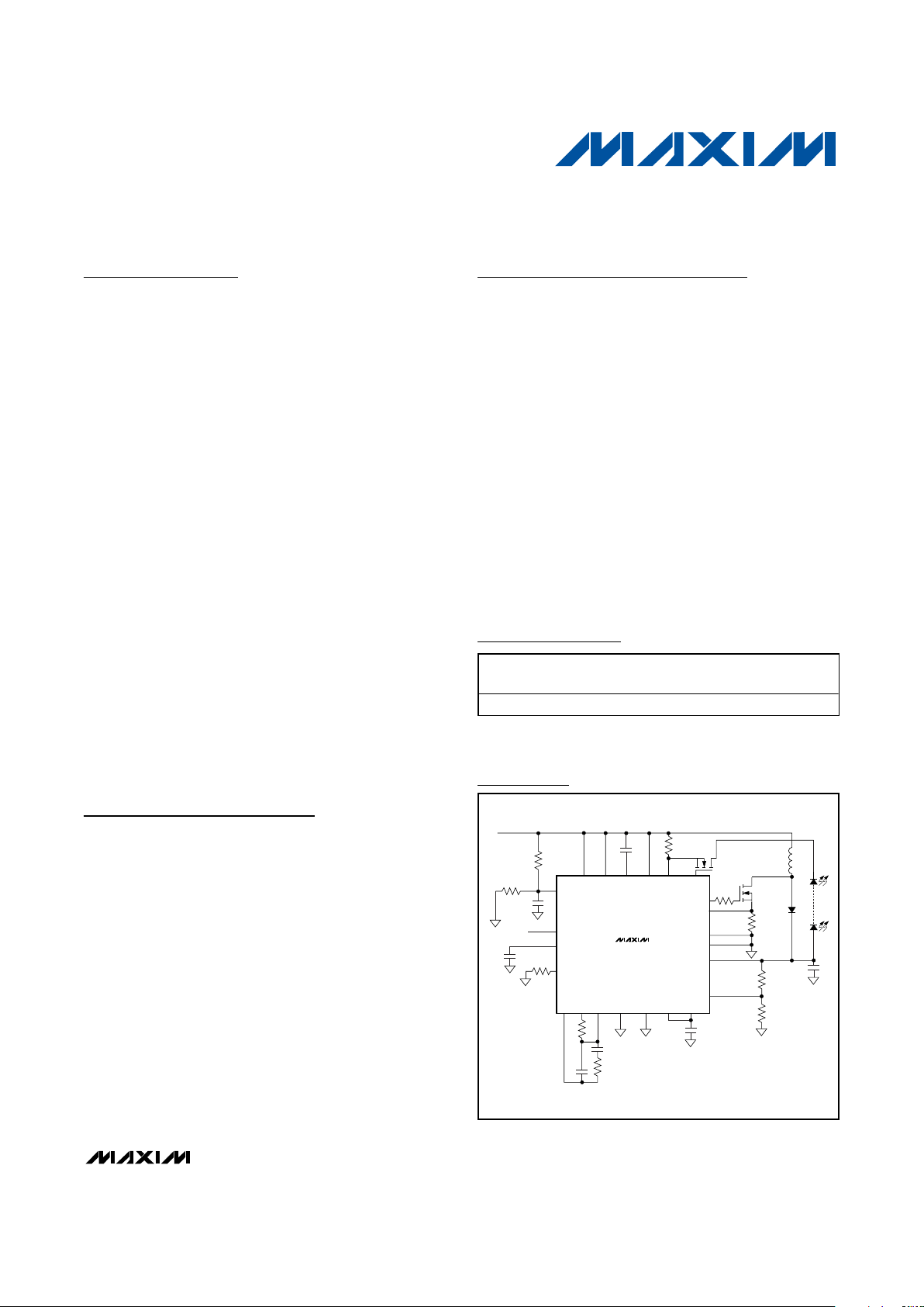
General Description
The MAX16831 is a current-mode, high-brightness LED
(HBLED) driver designed to control two external
n-channel MOSFETs for the single-string LED current
regulation. The MAX16831 integrates all the building
blocks necessary to implement fixed-frequency HBLED
drivers with wide-range dimming control. The
MAX16831 is configurable to operate as a step-down
(buck), step-up (boost), or step-up/-down (buck-boost)
current regulator.
Current-mode control with leading-edge blanking simplifies control-loop design. Internal slope compensation
stabilizes the current loop when operating at duty cycles
above 50%. The MAX16831 operates over a wide input
voltage range and is capable of withstanding automotive load-dump events. Multiple MAX16831s can be
synchronized to each other or to an external clock. The
MAX16831 includes a floating dimming driver for
brightness control with an external n-channel MOSFET
in series with the LED string.
HBLED drivers using the MAX16831 achieve efficiencies of over 90% in automotive applications. The
MAX16831 also includes a 1.4A source and 2.5A sink
gate driver for driving switching MOSFETs in high-power
LED driver applications, such as front light assemblies.
The dimming control allows for wide PWM dimming at
frequencies up to 2kHz. Higher dimming ratios of up to
1000:1 are achievable at lower dimming frequencies.
The MAX16831 is available in a 32-pin thin QFN package
with exposed pad and operates over the -40°C to
+125°C automotive temperature range.
Applications
Automotive Exterior Lighting:
High-Beam/Low-Beam/Signal Lights
Rear Combination Lights (RCL)
Daytime Running Lights (DRL)
Fog Light and Adaptive Front Light Assemblies
Industrial and Architectural Lighting
Emergency Lighting
Projectors with RGB LED Light Sources
Navigation and Marine Indicators
Features
o Wide Input Range: 6V to 76V With Cold-Start
Operation to 5.5V
o Integrated Differential LED Current-Sense
Amplifier
o Floating Dimming Driver Capable of Driving an
n-Channel MOSFET
o 5% LED Current Accuracy
o 200Hz On-Board Ramp Syncs to External PWM
Dimming Signal
o Programmable Switching Frequency (125kHz to
600kHz) and Synchronization
o Output Overvoltage Load Dump, LED Short,
Overtemperature Protection
o Low 107mV LED Current Sense for High
Efficiency
o Enable/Shutdown Input with Shutdown Current
Below 45µA
MAX16831
High-Voltage, High-Power LED Driver with
Analog and PWM Dimming Control
________________________________________________________________
Maxim Integrated Products
1
19-0809; Rev 0; 4/07
For pricing, delivery, and ordering information, please contact Maxim/Dallas Direct! at
1-888-629-4642, or visit Maxim’s website at www.maxim-ic.com.
Ordering Information
PART TEMP RANGE
PINPACKAGE
PKG
CODE
MAX16831ATJ+ -40°C to +125°C 32 TQFN-EP* T3255M-4
+
Denotes lead-free package.
*
EP = Exposed pad.
V
IN
DIM
R
CS
C
F
R
T
C
REG1
R
UV2
DRV
DRI
REG1
DIM
CS
V
CC
SNS+
FB
QGND
RTSYNC
CS-
CS+
LO
COMP
REG2
DGT
HI
OV
UVEN
SNS-
AGND
R
SENSE
R2
C2
R
OV1
R
OV2
CLMP
SGND
C
CLMP
C
REG2
R1
C1
R
D
LEDs
BUCK-BOOST CONFIGURATION
R
UV1
C
UVEN
Q
S
MAX16831
Typical Operating Circuits
Pin Configuration appears at end of data sheet.
Typical Operating Circuits continued at end of data sheet.
MAX16831
High-Voltage, High-Power LED Driver with
Analog and PWM Dimming Control
2 _______________________________________________________________________________________
ABSOLUTE MAXIMUM RATINGS
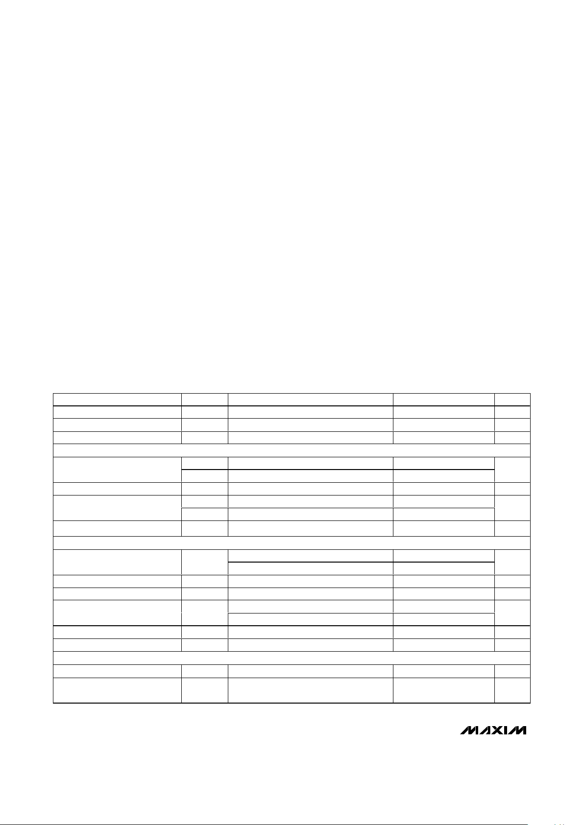
ELECTRICAL CHARACTERISTICS
(VCC= V
UVEN
= 14V, C
REG1
= 1µF, C
REG2
= 1µF, C
CLMP
= 0.1µF, RT= 25kΩ, TA= TJ = -40°C to +125°C, unless otherwise noted.
Typical specifications are at T
A
= +25°C.)
Stresses beyond those listed under “Absolute Maximum Ratings” may cause permanent damage to the device. These are stress ratings only, and functional
operation of the device at these or any other conditions beyond those indicated in the operational sections of the specifications is not implied. Exposure to
absolute maximum rating conditions for extended periods may affect device reliability.
VCC, HI, LO, CLMP to QGND.................................-0.3V to +80V
CS+, CS-, DGT, UVEN to QGND............................-0.3V to +80V
UVEN to QGND ..........................................-0.3V to (V
CC
+ 0.3V)
DRV to SGND .........................................................-0.3V to +18V
DRI, REG2, DIM to AGND ......................................-0.3V to +18V
QGND, SGND to AGND ........................................-0.3V to +0.3V
SNS+ to SNS- ...........................................................-0.3V to +6V
CS, FB, COMP, SNS+, SNS-, OV, REF,
RTSYNC to AGND .................................................-0.3V to +6V
REG1, CLKOUT to AGND ........................................-0.3V to +6V
CS+ to CS- .............................................................-0.3V to +12V
HI to LO ..................................................................-0.3V to +36V
CS+, CS-, DGT, CLMP to LO .................................-0.3V to +12V
CS+, CS-, DGT, CLMP to LO ........................-0.3V to (HI + 0.3V)
HI to CLMP .............................................................-0.3V to +28V
Continuous Power Dissipation* (T
A
= +70°C)
32-Pin TQFN (derate 34.5mW/°C above +70°C) ........2758mW
Thermal Resistance*
θ
JA
.................................................................................29°C/W
θ
JC
................................................................................1.7°C/W
Operating Temperature Range .........................-40°C to +125°C
Maximum Junction Temperature .....................................+150°C
Storage Temperature Range .............................-60°C to +150°C
Reflow Temperature.........................................................+240°C
Lead Temperature (soldering, 10s) .................................+300°C
*As per JEDEC 51 standard, multilayer board (PCB).
PARAMETER SYMBOL CONDITIONS MIN TYP MAX UNITS
Input Voltage Range V
CC
5.5 76.0 V
Supply Current I
Q
I
REG2
= 0A 2.7 4.5 mA
Shutdown Current I
SHDN
V
UVEN
≤ 0.8V 25 45 µA
UVEN
V
CC_R
VCC rising 5.5 6.0
VCC UVLO Threshold
V
CC_F
VCC falling 5.0 5.5
V
VCC Threshold Hysteresis V
CC_HYS
0.4 V
V
UVR
V
UVEN
rising 1.100 1.244 1.360
UVEN Threshold
V
UVF
V
UVEN
falling 1.000 1.145 1.260
V
UVEN Input Current I
UVEN
V
UVEN
= 0V and V
UVEN
= 76V, VCC = 77V -0.2 +0.2 µA
REGULATORS
0 ≤ I
REG1
≤ 2mA, 7.5V ≤ VCC ≤ 76V 4.75 5.00 5.25
REG1 Regulator Output V
REG1
I
REG1
= 2mA, VCC = 5.7V 4.00 4.50 5.25
V
REG1 Dropout Voltage I
REG1
= 2mA (Note 1) 0.5 1.0 V
REG1 Load Regulation ∆V/∆IVCC = 7.5V, 0 ≤ I
REG1
≤ 2mA 25 Ω
7.5V ≤ VCC ≤ 76V, I
REG2
= 1mA 6.65 7.00 7.35
REG2 Regulator Output V
REG2
VCC = 5.7V, 0 ≤ I
REG2
≤ 20mA 4.5 5.0
V
REG2 Dropout Voltage I
REG2
= 20mA (Note 1) 0.5 V
REG2 Load Regulation ∆V/∆IVCC = 7.5V, 0 ≤ I
REG2
≤ 20mA 25 Ω
HIGH-SIDE REGULATOR (CLMP) (All Voltages Referred to LO) (Note 2)
CLMP UVLO Threshold V
CLMPTHVCLMP
rising 2.0 2.5 3.0 V
CLMP UVLO Threshold
Hysteresis
V
CLMPHYS
0.22 V
MAX16831
High-Voltage, High-Power LED Driver with
Analog and PWM Dimming Control
_______________________________________________________________________________________ 3
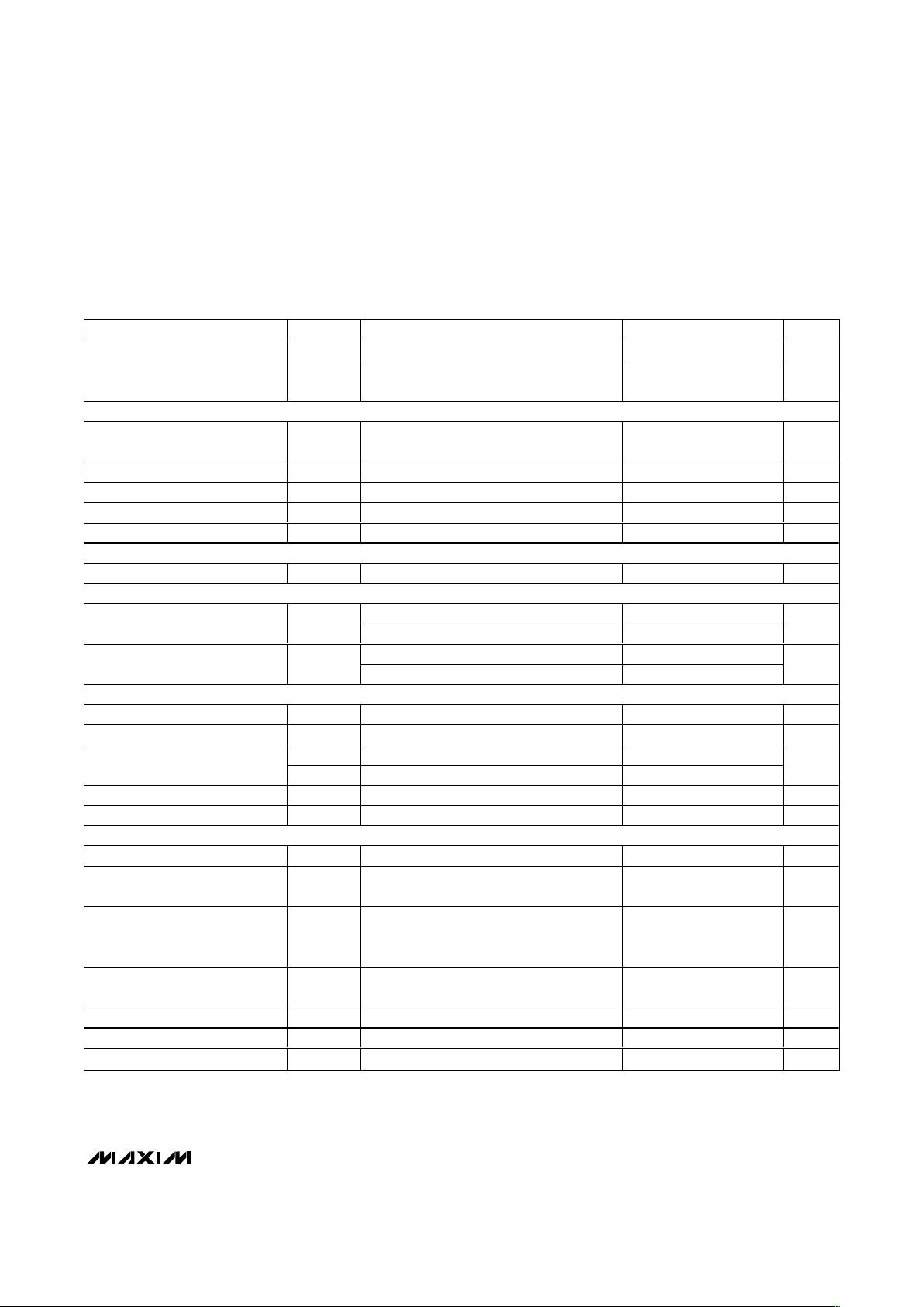
PARAMETER SYMBOL CONDITIONS MIN TYP MAX UNITS
8.7V ≤ (V
HI
- VLO) ≤ 36V, I
CLMP
= 1mA 5.5 8.0 10.0
CLMP Regulator Output Voltage V
CLMP
5.0V ≤ (VHI - VLO) ≤ 8.7V, I
CLMP
= 250µA
(V
HI
- VLO)
- 0.7
V
CURRENT-SENSE AMPLIFIER (CSA)
Differential Input Voltage Range
V
CS+
-
V
CS-
0 0.3 V
Common-Mode Range 0V
CC
V
CS+ Input Bias Current I
CS+
V
CS+
- V
CS-
= 0.3V -250 +250 µA
CS- Input Bias Current I
CS-
V
CS+
- V
CS-
= 0.3V 400 µA
Unity-Gain Bandwidth From (CS+ - CS-) to CS 1.0 MHz
REF OUTPUT BUFFER
REF Output Voltage V
REF
-100µA ≤ I
REF
≤ +100µA 2.85 3.00 3.15 V
DIM DRIVER
V
CLMP
- VLO = 4V 5 20
Source Current
V
CLMP
- VLO = 8V 30 67
mA
V
CLMP
- VLO = 4V 10 22
Sink Current
V
CLMP
- VLO = 8V 40 76
mA
GATE DRIVER
DRI UVLO Threshold V
UVLO_TH
DRI rising 4.0 4.2 4.4 V
DRI UVLO Threshold Hysteresis V
UVLO_HYST
0.3 V
Z
OUT_LVDRI
= 7.0V, DRV sinking 250mA 2.8 4
Driver Output Impedance
Z
OUT_HVDRI
= 7.0V, DRV sourcing 250mA 5.0 8
Ω
Peak Sink Current I
SK
V
DRI
= 7.0V 2.5 A
Peak Source Current I
SR
V
DRI
= 7.0V 1.4 A
PWM, ILIM, AND HICCUP COMPARATOR
PWM Comparator Offset Voltage V
COMP
- (V
SNS+
- V
SNS-)
0.7 V
Peak Current-Limit Comparator
Trip Threshold
160 200 240 mV
Peak Current-Limit Comparator
Propagation Delay (Excluding
Blanking Time)
50mV overdrive 40 ns
HICCUP Comparator Trip
Threshold
235 300 385 mV
SNS+ Input Bias Current V
SNS+
= 0V, V
SNS-
= 0V -100 -65 µA
SNS- Input Bias Current V
SNS+
= 0V, V
SNS-
= 0V -100 -65 µA
Blanking Time t
BLNK
40 ns
ELECTRICAL CHARACTERISTICS (continued)
(VCC= V
UVEN
= 14V, C
REG1
= 1µF, C
REG2
= 1µF, C
CLMP
= 0.1µF, RT= 25kΩ, TA= TJ = -40°C to +125°C, unless otherwise noted.
Typical specifications are at T
A
= +25°C.)
MAX16831
High-Voltage, High-Power LED Driver with
Analog and PWM Dimming Control
4 _______________________________________________________________________________________
ELECTRICAL CHARACTERISTICS (continued)
(VCC= V
UVEN
= 14V, C
REG1
= 1µF, C
REG2
= 1µF, C
CLMP
= 0.1µF, RT= 25kΩ, TA= TJ = -40°C to +125°C, unless otherwise noted.
Typical specifications are at T
A
= +25°C.)
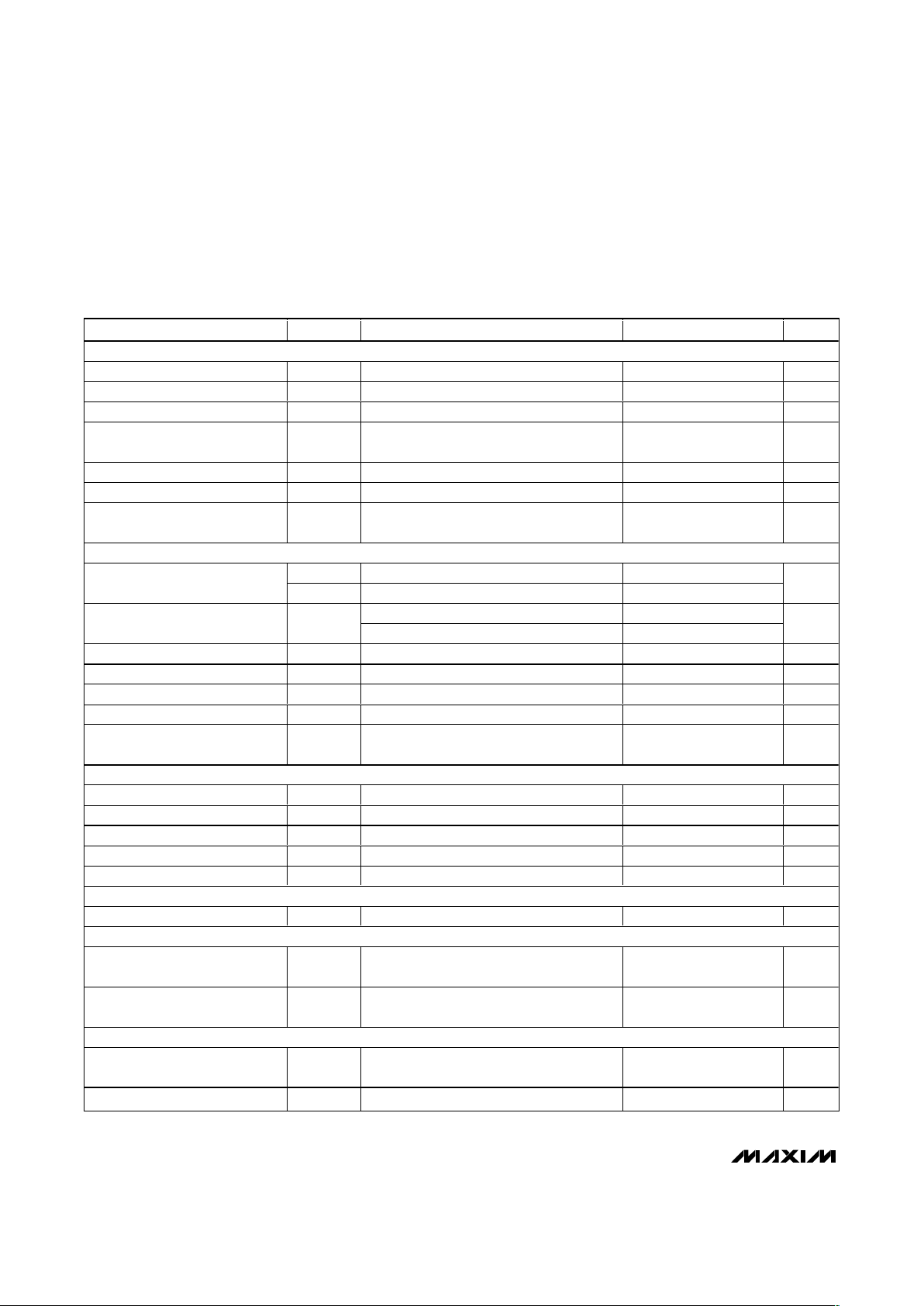
PARAMETER SYMBOL CONDITIONS MIN TYP MAX UNITS
ERROR AMPLIFIER
FB Input Bias Current -100 +100 nA
EAMP Output Sink Current VFB = 1.735V, V
COMP
= 1V 3 7 mA
EAMP Output Source Current VFB = 0.735V, V
COMP
= 1V 2 7 mA
EAMP Input Common-Mode
Voltage
0 3.0 V
EAMP Output Clamp Voltage 1.1 1.7 2.4 V
Voltage Gain A
V
R
COMP
= 100kΩ to AGND 80 dB
Unity-Gain Bandwidth GBW
R
COMP
= 100kΩ to AGND, C
COMP
= 100pF
to AGND
0.5 MHz
OSCILLATOR, OSC SYNC, CLK, AND CLKOUT
f
SWMIN
125
RTSYNC Frequency Range
f
SWMAX
500
kHz
RT = 25kΩ 475 500 525
RTSYNC Oscillator Frequency
R
T
= 100kΩ 106 125 143
kHz
RTSYNC High-Level Voltage V
SIHL
2.8 V
RTSYNC Low-Level Voltage V
SILL
0.4 V
CLKOUT High Level I
SINK
= 0.8mA 2.8 V
CLKOUT Low Level I
SOURCE
= 1.6mA 0.4 V
CLKOUT Maximum Load
Capacitance
C
CLK_CAPfSW
= 500kHz 500 pF
DIM SYNC, DIM RAMP, AND DIM PWM GEN
Internal Ramp Frequency f
RAMP
160 200 240 Hz
External Sync Frequency Range f
DIM
80 2000 Hz
External Sync Low-Level Voltage V
LTH
0.4 V
External Sync High-Level Voltage V
HTH
3.2 V
DIM Comparator Offset V
DIMOS
170 200 300 mV
DIGITAL SOFT-START
Soft-Start Duration t
SS
4.0 ms
OVERVOLTAGE COMPARATOR, LOAD OVERCURRENT COMPARATOR
OVP Overvoltage Comparator
Threshold
V
OV
VOV rising 1.20 1.235 1.27 V
OVP Overvoltage Comparator
Hysteresis
V
OV_HYST
63.5 mV
SLOPE COMPENSATION
Slope Compensation Peak
Voltage Per Cycle
Clock generated by R
T
120 mV
Slope Compensation External clock applied to RTSYNC 15 mV/µs
MAX16831
High-Voltage, High-Power LED Driver with
Analog and PWM Dimming Control
_______________________________________________________________________________________ 5
PARAMETER SYMBOL CONDITIONS MIN TYP MAX UNITS
THERMAL SHUTDOWN
Thermal Shutdown Temperature T
SHDN
Temperature rising +165 °C
Hysteresis ∆T
SHDN
20 °C
ELECTRICAL CHARACTERISTICS (continued)
(VCC= V
UVEN
= 14V, C
REG1
= 1µF, C
REG2
= 1µF, C
CLMP
= 0.1µF, RT= 25kΩ, TA= TJ = -40°C to +125°C, unless otherwise noted.
Typical specifications are at T
A
= +25°C.)
Note 1: Dropout voltage is defined as the input to output differential voltage at which the regulator output voltage drops 100mV below
the nominal output voltage.
Note 2: V
CLMPTH
determines the voltage required to operate the current-sense amplifier. The DIM driver requires 2.5V for (V
CLMP
- VLO)
to drive the external MOSFET. V
HI
is typically one diode drop above V
CLMP
. A large capacitor connected to V
CLMP
slows the
response of the LED current-sense circuitry, resulting in current overshoot. To ensure proper operation, connect a 0.1µF
capacitor from CLMP to LO.
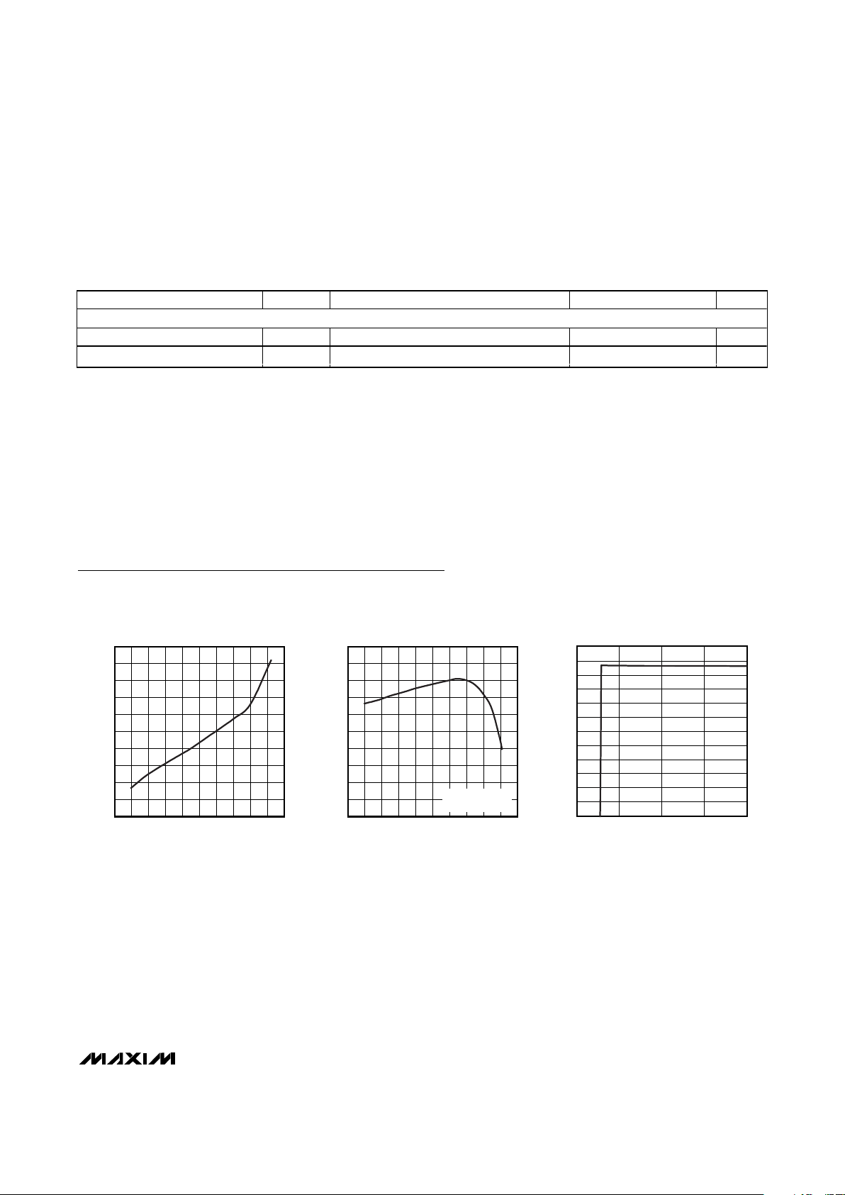
Typical Operating Characteristics
(VCC= V
UVEN
= 14V, C
REG1
= 1µF, C
REG2
= 10µF, C
CLMP
= 0.1µF, RT= 25kΩ, RCS= 0.1Ω, TA= +25°C, unless otherwise noted.)
18
20
19
22
21
24
23
25
27
26
28
-60 -20 0 20-40 40 60 80 120100 140
SHUTDOWN CURRENT
vs. TEMPERATURE
MAX16831 toc01
TEMPERATURE (°C)
SHUTDOWN CURRENT (µA)
2.0
2.2
2.1
2.4
2.3
2.6
2.5
2.7
2.9
2.8
3.0
-60 -20 0 20-40 40 60 80 120100 140
OPERATING CURRENT
vs. TEMPERATURE
MAX16831 toc02
TEMPERATURE (°C)
OPERATING CURRENT (mA)
DGT AND DRV NOT
SWITCHING
40
30
20
10
0
70
60
50
80
90
110
100
120
0 10203040
VOLTAGE ACROSS LED CURRENT-SENSE
RESISTOR vs. SUPPLY VOLTAGE
MAX16831 toc03
SUPPLY VOLTAGE (V)
VOLTAGE ACROSS R
CS
(mV)
MAX16831
High-Voltage, High-Power LED Driver with
Analog and PWM Dimming Control
6 _______________________________________________________________________________________
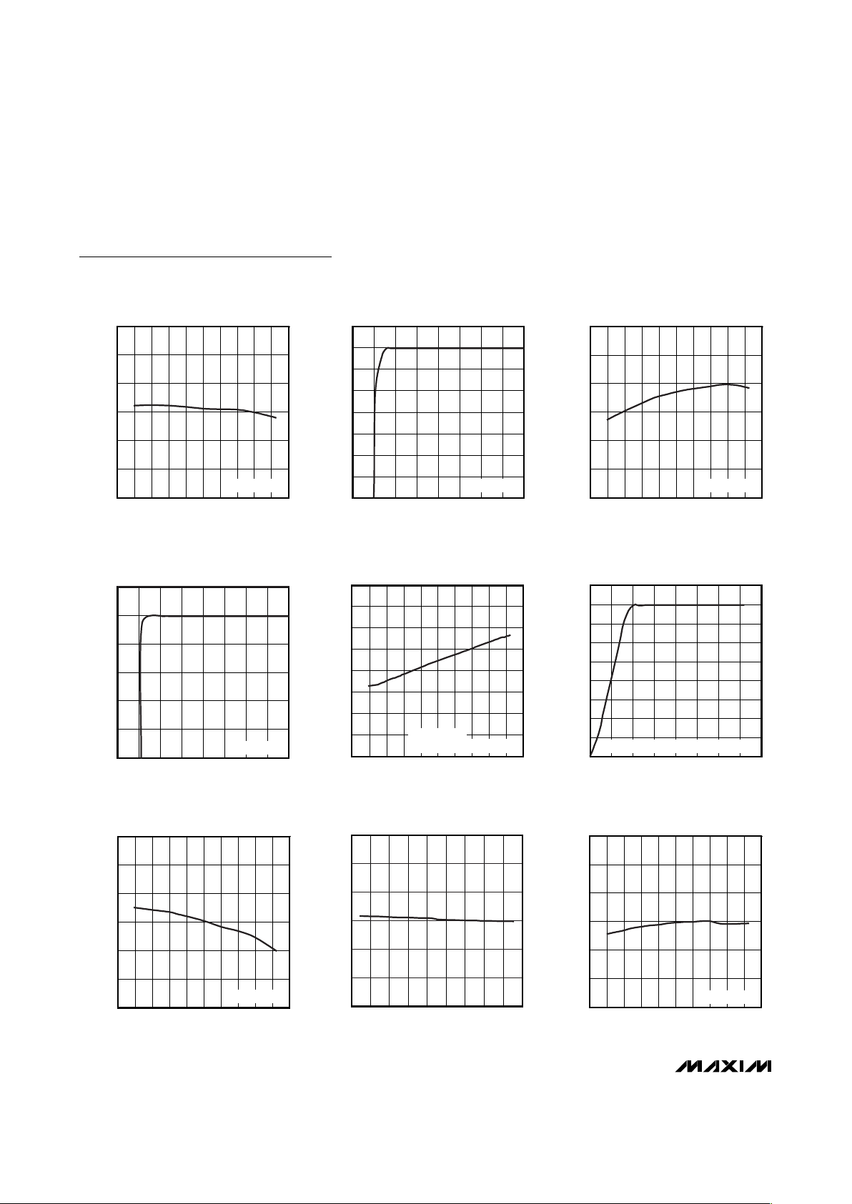
Typical Operating Characteristics (continued)
(VCC= V
UVEN
= 14V, C
REG1
= 1µF, C
REG2
= 10µF, C
CLMP
= 0.1µF, RT= 25kΩ, RCS= 0.1Ω, TA= +25°C, unless otherwise noted.)
6.80
6.95
6.90
6.85
7.00
7.05
7.10
-60 200-40 -20 40 60 80 100 120 140
REG2 OUTPUT VOLTAGE
vs. TEMPERATURE
MAX16831 toc04
TEMPERATURE (°C)
REG2 OUTPUT VOLTAGE (V)
I
REG2
= 20mA
0
2
1
4
3
5
6
7
8
010155 2025303540
REG2 OUTPUT VOLTAGE
vs. SUPPLY VOLTAGE
MAX16831 toc05
SUPPLY VOLTAGE (V)
REG2 OUTPUT VOLTAGE (V)
I
REG2
= 20mA
4.90
4.96
4.94
4.92
4.98
5.00
5.02
-60 200-40 -20 40 60 80 100 120 140
REG1 OUTPUT VOLTAGE
vs. TEMPERATURE
MAX16831 toc06
TEMPERATURE (°C)
REG1 OUTPUT VOLTAGE (V)
I
REG1
= 2mA
0
1
2
3
4
5
6
0105 152025303540
REG1 OUTPUT VOLTAGE
vs. SUPPLY VOLTAGE
MAX16831 toc07
SUPPLY VOLTAGE (V)
REG1 OUTPUT VOLTAGE (V)
I
REG1
= 2mA
7.5
7.7
7.6
7.8
8.1
8.2
8.0
7.9
8.3
-60 -20 0 20 40-40 60 80 100 120 140
CLMP REGULATOR VOLTAGE
vs. TEMPERATURE
MAX16831 toc08
TEMPERATURE (°C)
CLMP VOLTAGE (V)
VHI - VLO = 11V
CLMP VOLTAGE = V
CLMP
- VLO
1
3
2
5
4
6
7
8
9
010155 2025303540
CLMP REGULATOR VOLTAGE
vs. (V
HI
- VLO)
MAX16831 toc09
VHI - VLO (V)
CLMP REGULATOR VOLTAGE (V)
CLMP REGULATOR VOLTAGE = V
CLMP
- V
LO
2.96
2.99
2.98
2.97
3.00
3.01
3.02
-60 200-40 -20 40 60 80 100 120 140
REF OUTPUT VOLTAGE
vs. TEMPERATURE
MAX16831 toc10
TEMPERATURE (°C)
REF OUTPUT VOLTAGE (V)
I
REF
= 100µA
2.96
2.97
2.99
2.98
3.01
3.00
3.02
-225 -125 -75-175 -25 25 75 125 175 225
REF OUTPUT VOLTAGE
vs. LOAD CURRENT
MAX16831 toc11
LOAD CURRENT (µA)
REF OUTPUT VOLTAGE (V)
470
500
490
480
510
520
530
-60 200-40 -20 40 60 80 100 120 140
PWM OSCILLATOR FREQUENCY
vs. TEMPERATURE
MAX16831 toc12
TEMPERATURE (°C)
PWM FREQUENCY (kHz)
RT = 25kΩ
 Loading...