

General Description
The MAX16824/MAX16825 three-channel LED drivers
operate over a 6.5V to 28V input voltage range. These
devices provide three open-drain constant-current-sinking outputs that are rated to 36V and deliver up to
150mA of current to each string of high-brightness LEDs
(HB LEDs). The current at each output is programmable
by means of an external current-sense resistor. The
MAX16824 features three PWM inputs that control the
duty cycle of the output current, allowing a wide LED
dimming range to be implemented. The PWM inputs
also function as on/off control for each corresponding
output. The MAX16825 offers a 2Mbps, 4-wire serial
interface, a 3-bit shift register, and a 3-bit transparent
latch. The serial interface allows a microcontroller to
configure the output channels using four inputs (DIN,
CLK, LE, OE) and a data output (DOUT). DOUT allows
multiple drivers to be cascaded and operated together.
The MAX16824/MAX16825’s on-board pass elements
minimize the need for external components, while at the
same time, providing ±5% LED current accuracy.
Additional features include a +5V (±5%) regulated output
with 4mA output current capability and thermal protection.
The MAX16824/MAX16825 are available in a thermally
enhanced 16-pin TSSOP-EP package and specified over
the -40°C to +85°C temperature range.
Applications
Industrial Lighting
Architectural and Decorative Lighting
Mood Lighting
Indoor and Outdoor LED Video Displays
Automotive Lighting
LCD Display Backlighting
Features
♦ 6.5V to 28V Operating Range
♦ Outputs Connected to 36V Supply for Long LED
Strings
♦ Three 36V-Rated Output Channels with
Independently Adjustable LED Current
♦ 150mA Output Current Per Channel
♦ ±5% LED Current Accuracy
♦ PWM Dimming
Three Independent Dimming Control Inputs
(MAX16824)
4-Wire Serial Interface LED Current Chopping
(MAX16825)
♦ +5V (±5%) Regulated Output with 4mA Source
Capability
♦ Fast Transient Dimming Response
♦ 200mV Current-Sense Reference Reduces Power
Loss
♦ Thermal Shutdown
♦ -40°C to +85°C Operating Temperature Range
♦ Thermally Enhanced, 16-Pin TSSOP Exposed
Paddle Package
MAX16824/MAX16825
High-Voltage, Three-Channel Linear
High-Brightness LED Drivers
________________________________________________________________
Maxim Integrated Products
1
19-1107; Rev 0; 11/07
For pricing, delivery, and ordering information, please contact Maxim Direct at 1-888-629-4642,
or visit Maxim's website at www.maxim-ic.com.
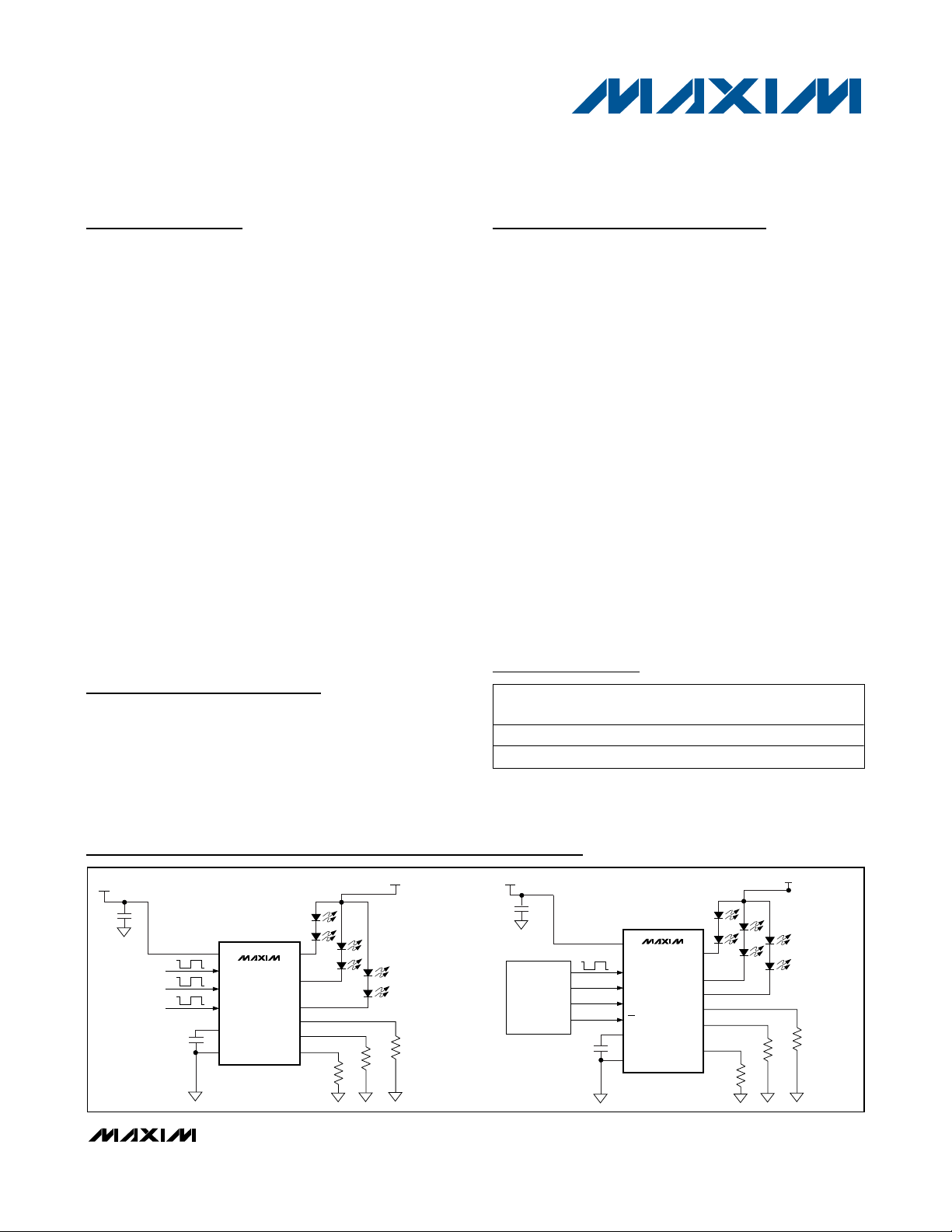
OUT1
OUT3
OUT2
CS1
CS2
CS3
IN
1
16
3
7
8
9
4
11
12
2
15
13
PWM1
PWM2
PWM3
REG
GND
C
REG
C
IN
V
IN
UP TO 36V
R
CS2
R
CS1
R
CS3
MAX16824
Typical Operating Circuits
Ordering Information
+
Denotes a lead-free package.
*
EP = Exposed paddle.
Pin Configurations appear at end of data sheet.
PART TEMP RANGE
PIN
PACKAGE
MAX16824EUE+ -40°C to +85°C 16 TSSOP-EP* U16E-3
MAX16825EUE+ -40°C to +85°C 16 TSSOP-EP* U16E-3
PKG
CODE
V
IN
C
IN
3
IN
MAX16825
6
CLK
7
DIN
MICROCONTROLLER
8
LE
9
OE
4
C
REG
REG
11
GND
1
OUT1
16
OUT2
12
OUT3
2
CS1
15
CS2
13
CS3
UP TO 36V
R
CS1
R
CS2
R
CS3
MAX16824/MAX16825
High-Voltage, Three-Channel Linear
High-Brightness LED Drivers
2 _______________________________________________________________________________________
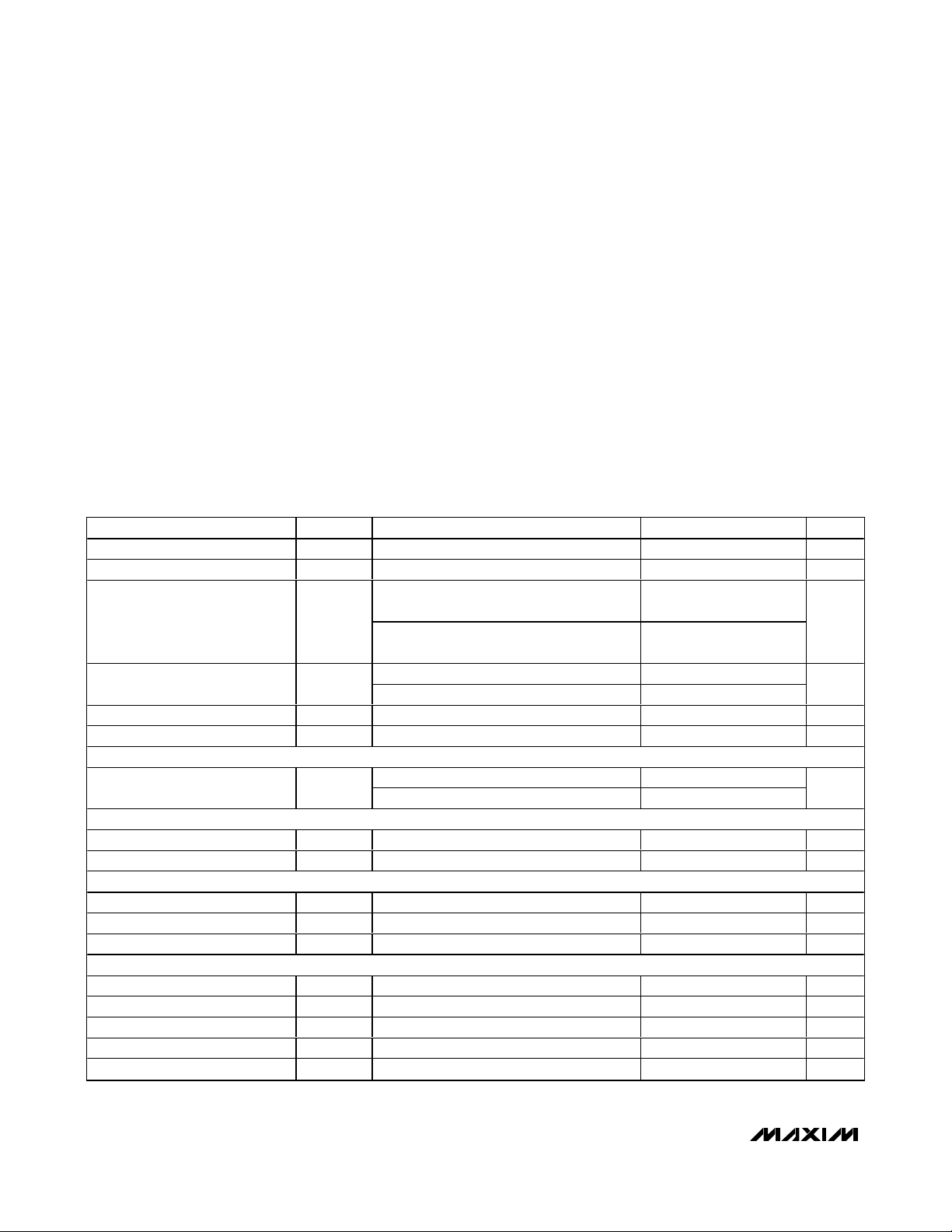
ABSOLUTE MAXIMUM RATINGS
Stresses beyond those listed under “Absolute Maximum Ratings” may cause permanent damage to the device. These are stress ratings only, and functional
operation of the device at these or any other conditions beyond those indicated in the operational sections of the specifications is not implied. Exposure to
absolute maximum rating conditions for extended periods may affect device reliability.
IN to GND ...............................................................-0.3V to +30V
OUT1, OUT2, OUT3 to GND ..................................-0.3V to +40V
CS1, CS2, CS3, REG to GND...................................-0.3V to +6V
PWM1, PWM2, PWM3 to GND .................................-0.3V to +6V
DIN, CLK, LE, OE, DOUT to GND ............................-0.3V to +6V
Maximum Current into Any Pin
(except OUT1, OUT2, OUT3) ........................................±20mA
Maximum Current into OUT1, OUT2, OUT3......................160mA
Continuous Power Dissipation (T
A
= +70°C)
16-Pin TSSOP-EP (derate 18.9mW/°C above +70°C)....1500mW
Operating Temperature Range ...........................-40°C to +85°C
Junction Temperature......................................................+150°C
Storage Temperature Range .............................-65°C to +150°C
Lead Temperature (soldering, 10s) .................................+300°C
ELECTRICAL CHARACTERISTICS
(VIN= 12V, C
REG
= 1µF to GND, I
REG
= 0, R
CS_
= 2Ω from CS_ to GND, TJ= TA= -40°C to +85°C, unless otherwise noted. Typical
values are at T
J
= TA= +25°C.) (Note 1)
Supply Voltage Range V
GND Current I
LED Current-Sense Accuracy
(Note 2)
Dropout Voltage (Note 3) ΔV
Output Current Slew Rate Current rising, V
Output Current Leakage I
CURRENT SENSE
Regulated CS_ Voltage V
OVERTEMPERATURE PROTECTION
Thermal Shutdown Temperature 165 °C
Thermal Shutdown Hysteresis 23 °C
+5V REGULATOR (REG)
Output Voltage V
REG Output Current I
REG Short-Circuit Current I
LOGIC INPUT (PWM1, PWM2, PWM3)
PWM_ Input Bias Current I
PWM_ Input-Voltage High V
PWM_ Input-Voltage Low V
PWM_ Turn-On Delay 50% of V
PWM_ Turn-Off Delay 50% of V
PARAMETER SYMBOL CONDITIONS MIN TYP MAX UNITS
IN
I
GND
OUT1
10mA < I
0°C ≤ T
10mA < I
-40°C ≤ T
I
DO
LEAK
CS_
REGIREG
REG
REGSCVREG
PWM
IH
IL
OUT_
I
OUT_
PWM1 = PWM2 = PWM3 = 0V 1 µA
V
CS1
V
CS1
4.75V < V
V
PWM1
= I
= 100mA (current pulsed) 0.75 1.5
= 150mA (current pulsed) 1.2 2.25
= V
= V
= 0mA (Note 4) 4.75 5 5.25 V
= 0V (Note 5) 15 40 90 mA
OUT2
OUT_
≤ 85°C
J
OUT_
≤ 85°C
J
CS2
CS2
REG
= V
PWM_
PWM_
= I
OUT3
< 100mA,
< 100mA,
OUT
= V
CS3
= V
CS3
= V
PWM2
to 50% of ΔV
to 50% of ΔV
=100mA 5 10 mA
= 4V 100 mA/µs
, 0°C ≤ TJ ≤ +85°C 190 200 210
, -40°C ≤ TJ ≤ +85°C 186 200 214
= 5V 1 µA
PWM3
OUT_
OUT_
6.5 28.0 V
5
7
4mA
4V
0.6 V
475 ns
150 ns
%
V
mV
MAX16824/MAX16825
High-Voltage, Three-Channel Linear
High-Brightness LED Drivers
_______________________________________________________________________________________ 3
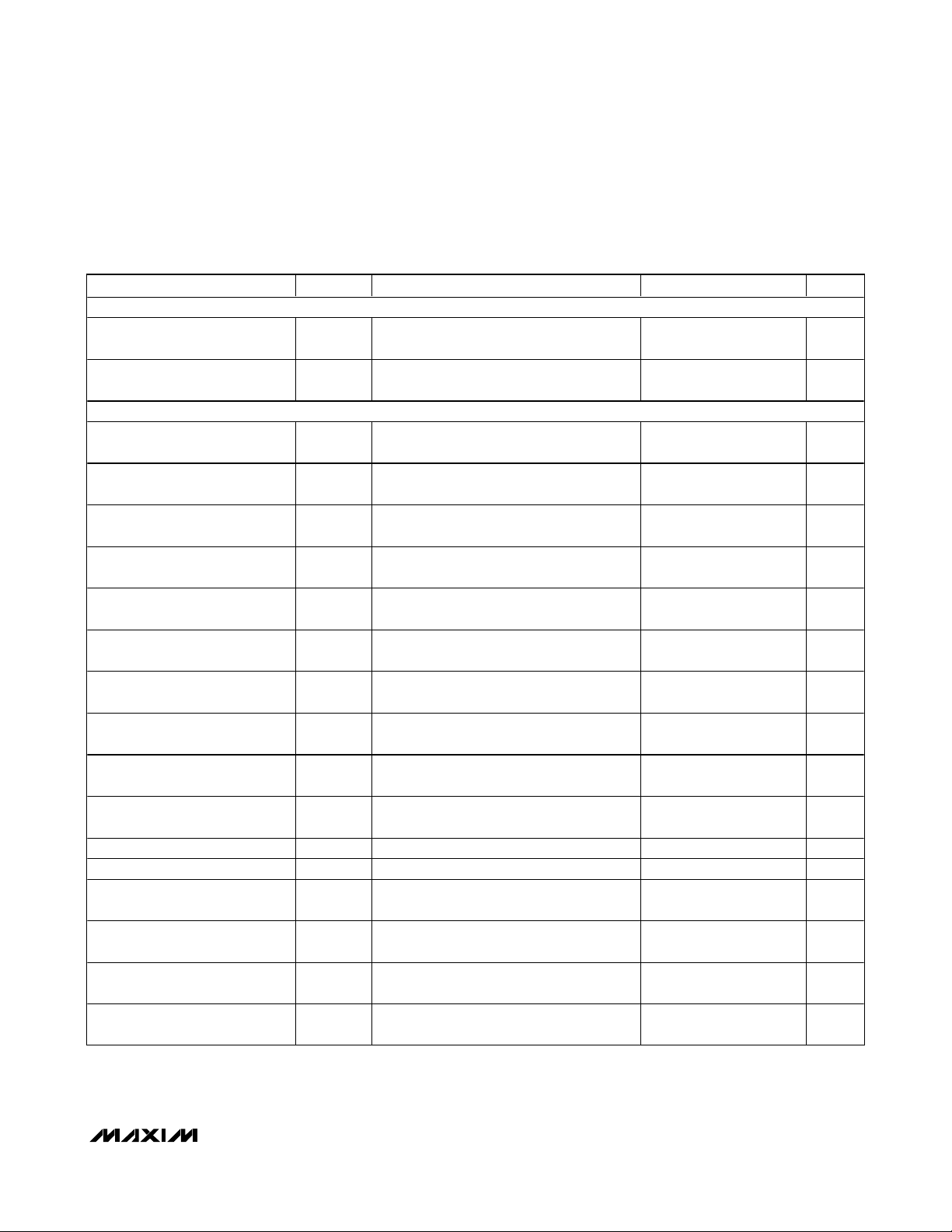
ELECTRICAL CHARACTERISTICS (continued)
(VIN= 12V, C
REG
= 1µF to GND, I
REG
= 0, R
CS_
= 2Ω from CS_ to GND, TJ= TA= -40°C to +85°C, unless otherwise noted. Typical
values are at T
J
= TA= +25°C.) (Note 1)
OUTPUTS (OUT1, OUT2, OUT3)
Turn-On Time t
Turn-Off Time t
SPI INTERFACE (CLK, LE, OE, DIN, DOUT) (Figures 3 and 4)
DIN, CLK, LE, OE Input Bias
Current
DIN, CLK, LE, OE Input-Voltage
High
DIN, CLK, LE, OE Input-Voltage
Low
CLK Clock Period t
CLK Pulse-Width High t
CLK Pulse-Width Low t
DIN Setup Time t
DIN Hold Time t
DOUT Propagation Delay t
DOUT Rise/Fall Time tDR/t
DOUT Voltage High V
DOUT Voltage Low V
LE Pulse-Width High t
LE Setup Time t
LE Rising to OUT_ Rising Delay t
LE Rising to OUT_ Falling Delay t
PARAMETER SYMBOL CONDITIONS MIN TYP MAX UNITS
R
F
V
IH
V
IL
CP
CH
CL
DS
DH
DO
DOH
DOL
LW
LS
LRR
LRF
PWM_ rising time, tR, is measured from 20%
to 80% of I
PWM_ falling time, tF, is measured from
80% to 20% of I
DIN = CLK = LE = OE = 0 or 5V 1 µA
50% of CLK rising to 50% of next CLK
rising, Figure 3
50% of CLK rising to 50% of CLK falling,
Figure 3
50% of CLK falling to 50% of CLK rising,
Figure 3
50% of DIN rising to 50% of CLK rising,
Figure 3
50% of CLK rising to 50% of DIN falling,
Figure 3
50% of CLK rising to 50% of DOUT rising/
falling, Figure 3
C
DOUT
DF
rising/falling edge (Note 6)
I
SOURCE
I
SINK
50% of LE rising to 50% of LE falling,
Figure 3
50% of CLK rising to 50% of LE rising,
Figure 3
50% of LE rising to 50% of OUT_ rising,
Figure 4
50% of LE rising to 50% of OUT_ falling,
Figure 4
OUT
OUT
= 10pF, 10% to 90% of DOUT
= 4mA 4.5 V
= 4mA 0.5 V
1µs
1µs
2.2 V
0.5 V
50 ns
24 ns
24 ns
5ns
10 ns
5ns
15 ns
20 ns
15 ns
150 ns
475 ns
MAX16824/MAX16825
High-Voltage, Three-Channel Linear
High-Brightness LED Drivers
4 _______________________________________________________________________________________
ELECTRICAL CHARACTERISTICS (continued)
(VIN= 12V, C
REG
= 1µF to GND, I
REG
= 0, R
CS_
= 2Ω from CS_ to GND, TJ= TA= -40°C to +85°C, unless otherwise noted. Typical
values are at T
J
= TA= +25°C.) (Note 1)
Note 1: All devices are 100% production tested at TJ= +25°C and TJ= +85°C. Limits to -40°C are guaranteed by design.
Note 2: This specification does not include sense resistor tolerance and ground error.
Note 3: Dropout is measured as follows: R
SC_
= 1.21Ω from CS_ to GND. Force 100mA into OUT_ and measure the dropout voltage
from OUT_ to CS_. DVDO = (ΔOUT_ - V
CS_
).
Note 4: OUT’s current regulation varies with load across REG (see the
Typical Operating Characteristics
).
Note 5: Overtemperature protection does not function if the output of the 5V reference (REG) is shorted to ground.
Note 6: Guaranteed by design, not production tested.
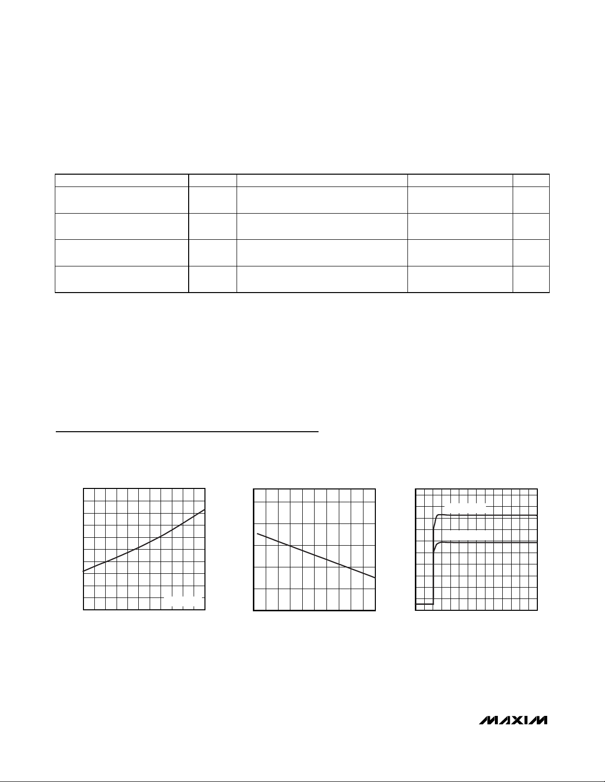
0
0.2
0.1
0.5
0.4
0.3
0.6
0.7
0.9
0.8
1.0
-40 -10 5-25 203550658095110125
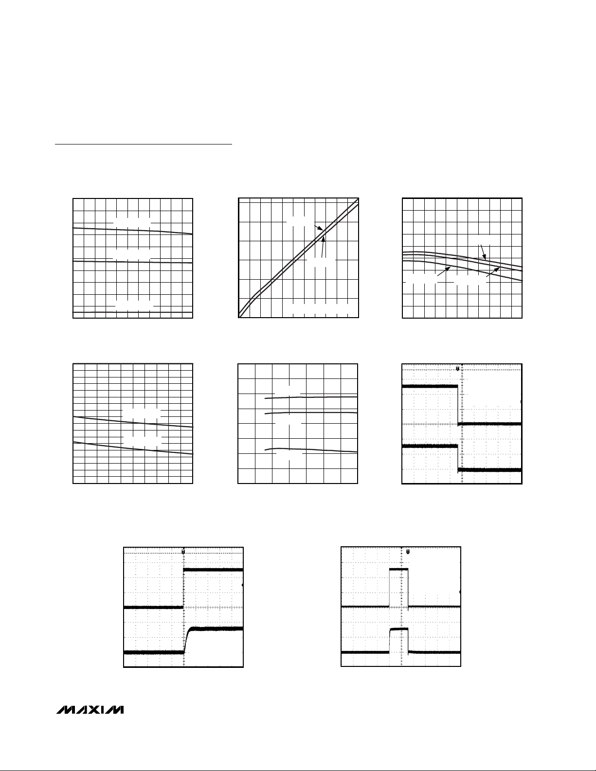
DROPOUT VOLTAGE vs. TEMPERATURE
MAX16824toc01
TEMPERATURE (°C)
DROPOUT VOLTAGE (V)
I
LOAD
= 100mA
0.182
0.192
0.187
0.197
0.202
0.207
0604515 30 75 90 105 120 135 150
CS_ VOLTAGE vs. OUTPUT CURRENT
MAX16824 toc02
OUTPUT CURRENT (mA)
V
CS_
(V)
OUTPUT CURRENT vs. INPUT VOLTAGE
MAX16824 toc03
VIN (V)
OUTPUT CURRENT (mA)
262420 226 8 10 12 14 16 182 4
10
30
50
70
90
110
130
150
170
190
-10
028
I
LOAD
= 150mA
I
LOAD
= 100mA
Typical Operating Characteristics
(VIN= 12V, C
REG
= 1µF to GND, I
REG
= 0, R
CS_
= 2Ω from CS_ to GND, TA= +25°C, unless otherwise noted. Typical values are at
TA= +25°C.)
CLK Rising to OUT_ Rising Delay t
CLK Rising to OUT_ Falling Delay t
OE Rising to OUT_ Rising Delay t
OE Falling to OUT_ Falling Delay t
PARAMETER SYMBOL CONDITIONS MIN TYP MAX UNITS
CRR
CRF
OEH
OEL
50% of CLK rising to 50% of OUT_ rising,
Figure 4
50% of CLK rising to 50% of OUT_ falling,
Figure 4
50% of OE rising to 50% of OUT_ rising,
Figure 3
50% of OE falling to 50% of OUT_ falling,
Figure 3
150 ns
475 ns
150 ns
475 ns
MAX16824/MAX16825
High-Voltage, Three-Channel Linear
High-Brightness LED Drivers
______________________________________________________________________________________________________________________________________________________________________________
5
Typical Operating Characteristics (continued)
(VIN= 12V, C
REG
= 1µF to GND, I
REG
= 0, R
CS_
= 2Ω from CS_ to GND, TA= +25°C, unless otherwise noted. Typical values are at
T
A
= +25°C.)
OUTPUT CURRENT vs. TEMPERATURE
200
180
160
140
120
100
80
60
OUTPUT CURRENT (mA)
40
20
0
-40 -10 5-25 203550658095110125
CS_ VOLTAGE vs. REG OUTPUT CURRENT
0.200
0.199
0.198
0.197
0.196
0.195
0.194
0.193
0.192
(V)
0.191
CS_
V
0.190
0.189
0.188
0.187
0.186
0.185
0.184
0.183
0.182
010
I
= 150mA
OUT
I
= 95mA
OUT
I
= 10mA
OUT
TEMPERATURE (°C)
I
LOAD
I
LOAD
I
(mA)
REG
= 100mA
= 150mA
986 72 3 4 51
MAX16824toc04
MAX16824 toc07
(V)
V
3.45
3.25
3.05
2.85
2.65
SUPPLY CURRENT (mA)
2.45
2.25
-40 125
OUTPUT VOLTAGE vs. INPUT VOLTAGE
5.000
4.995
4.990
4.985
4.980
REG
4.975
4.970
4.965
4.960
028
SUPPLY CURRENT
vs. TEMPERATURE
VIN = 28V
VIN = 6.5V
V
= V
PWM
PWM
TEMPERATURE (°C)
I
= 0
REG
I
= 1mA
REG
I
= 4mA
REG
VIN (V)
OUTPUT VOLTAGE vs. TEMPERATURE
5.10
5.08
MAX16824 toc05
5.06
5.04
5.02
(V)
5.00
REG
V
4.98
I
= 4mA
LOAD
4.96
4.94
= V
= 0
PWM
1109580655035205-10-25
4.92
4.90
TEMPERATURE (°C)
LED CURRENT FALL TIME
MAX16824 toc08
24204 8 12 16
I
LOAD
I
= 1mA
LOAD
I
LED
V
IN
PULSED AT 200Hz
(50% DUTY CYCLE)
2μs/div
= 0
= 150mA
= 12V
MAX16824 toc09
1109580655035205-10-25-40 125
MAX16824 toc06
V
PWM_
2V/div
0V
I
OUT_
100mA/div
0A
LED CURRENT RISE TIME
I
= 150mA
LED
= 12V
V
IN
PULSED AT 200Hz
(50% DUTY CYCLE)
2μs/div
MAX16824 toc10
V
PWM_
2V/div
0V
I
OUT_
100mA/div
0A
330Hz DIMMED OPERATION
20μs/div
MAX16824 toc11
I
= 150mA
LOAD
= 12V
V
IN
PWM_ PULSED
AT 330Hz
(1% DUTY CYCLE)
V
PWM_
2V/div
0V
I
OUT_
100mA/div
0A

MAX16824/MAX16825
High-Voltage, Three-Channel Linear
High-Brightness LED Drivers
6 _______________________________________________________________________________________
Pin Description
PIN
MAX16824 MAX16825
1 1 OUT1
2 2 CS1
3 3 IN Positive Input Supply. Bypass with a 0.1µF (min) capacitor to GND.
4 4 REG +5V-Regulated Output. Connect a 1µF capacitor from REG to GND.
5, 6, 10, 14 5, 14 N.C. No Connection. Must be left unconnected.
7 — PWM1
8 — PWM2
9 — PWM3
11 11 GND Ground
12 12 OUT3
13 13 CS3
15 15 CS2
16 16 OUT2
—7DIN
NAME FUNCTION
Channel 1 LED Driver Output. OUT1 is an open-drain, constant-current-sinking output
rated to 36V.
Channel 1 Sense Amplifier Negative Input. Connect a current-sense resistor between
CS1 and GND to program the output current level for channel 1.
Dimming Input 1. PWM1 is a dimming input for channel 1. A logic-low turns off OUT1 and
a logic-high turns on OUT1.
Dimming Input 2. PWM2 is a dimming input for channel 2. A logic-low turns off OUT2 and
a logic-high turns on OUT2.
Dimming Input 3. PWM3 is a dimming input for channel 3. A logic-low turns off OUT3 and
a logic-high turns on OUT3.
Channel 3 LED Driver Output. OUT3 is an open-drain, constant-current-sinking output
rated to 36V.
Channel 3 Sense Amplifier Negative Input. Connect a current-sense resistor between
CS3 and GND to program the output current level for channel 3.
Channel 2 Sense Amplifier Negative Input. Connect a current-sense resistor between
CS2 and GND to program the output current level for channel 2.
Channel 2 LED Driver Output. OUT2 is an open-drain, constant-current-sinking output
rated to 36V.
Serial-Data Input. Data is loaded into the internal 3-bit shift register on the rising edge of
CLK.
Latch-Enable Input. Data loaded transparently from the internal shift register to the
—8LE
—9OE
—10DOUT
— 6 CLK Clock Input
——EP
output latch while LE is high. Data is latched into the output latch on the LE’s falling edge
and retained while LE is low.
Output Enable Input. Drive OE high to place all outputs into a high-impedance mode
without altering the contents of the output latches. Drive OE low to force all outputs to
follow the state of the output latches.
Serial-Data Output. Data is clocked out of the internal 3-bit shift register to DOUT on the
rising edge of CLK. DOUT is a replica of the shift register’s last bit.
Exposed Paddle. Connect EP to a large-area ground plane for effective power
dissipation. Do not use as the IC ground connection.

Detailed Description
The MAX16824/MAX16825 are three-channel LED drivers that operate from a 6.5V to 28V input voltage
range. These devices provide three independent opendrain, constant-current-sinking outputs rated to 36V
and deliver up to 150mA of current to each HB LED
string. The current in each channel is programmable
using an external current-sense resistor in series with
each internal power MOSFET’s source. The MAX16824
features three separate PWM inputs that allow a wide
range of independent dimming level at each of the
three outputs. The PWM inputs also function as on/off
control inputs for each corresponding output (Figure 1).
The MAX16825 includes a 2Mbps, 4-wire serial interface to control the state of each output (Figure 2).
The 4-wire serial interface comprises a 3-bit shift register and a 3-bit transparent latch. The shift register is
updated using a clock input CLK and a data input DIN.
DOUT is the last bit of the shift register. This feature
allows multiple drivers to be cascaded and operated
together. The latch is transparent from the shift register
outputs to the LED output when LE is high while it latches the shift register state on the falling edge of LE. The
output-enable input OE allows simultaneous enabling
or disabling of all three outputs.
MAX16824/MAX16825
High-Voltage, Three-Channel Linear
High-Brightness LED Drivers
_______________________________________________________________________________________ 7
REG
Figure 1. Internal Block Diagram (MAX16824)
OUT1
THERMAL
SHUTDOWN
200mV
CS1
OUT2
CS2
OUT3
IN
BANDGAP AND
5V REGULATOR
PWM1
PWM
PWM2
PWM3
CONTROL AND
LOGIC
GND
CS3
MAX16824

MAX16824/MAX16825
High-Voltage, Three-Channel Linear
High-Brightness LED Drivers
8 _______________________________________________________________________________________
Figure 2. Internal Block Diagram (MAX16825)
IN
BANDGAP AND
5V REGULATOR
REG
THERMAL
SHUTDOWN
DIN
CLK
OUT1
200mV
CS1
OUT2
CS2
OUT3
CS3
DOUT
OE
SHIFT
REGISTER
LE
LATCH
SHIFT
REGISTER
LATCH
LOGIC
SHIFT
REGISTER
LATCH
MAX16825
GND

On-board pass elements minimize the need for external
components while providing ±5% LED current accuracy. Additional features include a +5V (±5%) regulated
output with 4mA output current capability and thermal
protection.
The MAX16824/MAX16825 use a feedback loop to linearly control the current at each output. The voltage
across each sense resistor is regulated to 200mV by
the internal feedback loop. The output current is set by
selecting the value of RCS.
+5V Regulator (REG)
The MAX16824/MAX16825 include a fixed +5V output
regulator that delivers up to 4mA of load current for
auxiliary low power applications throughout the 6.5V to
28V input voltage range. Connect a 1µF compensation
capacitor from REG to ground.
Thermal Protection
The MAX16824/MAX16825 enter a thermal shutdown
mode in the event of overheating. When the junction
temperature exceeds T
J
= +165°C, the internal thermal
protection circuit turns off the series pass elements.
The MAX16824/MAX16825 recover from thermal shutdown mode when the junction temperature drops by
23°C. The thermal protection does not operate if the
regulator (REG) is in a short-circuit condition.
4-Wire Serial Interface (MAX16825)
The MAX16825 features a 4-wire serial interface (DIN,
CLK, LE, OE) and a data output (DOUT) that allows the
use of a microcontroller to write brightness data to the
MAX16825. The serial-interface data word length is 3
bits (D0, D1, D2). The functions of the interface inputs
are as follows: DIN is the serial-data input, which must
be stable when it is sampled by the MAX16825 on the
rising edge of CLK. Data shifts in with the MSB first.
This means that data bit D2 is clocked in first, followed
by 2 more data bits (D1 and finishing with the LSB D0).
CLK is the serial-clock input, which shifts data at DIN
into the MAX16825’s 3-bit shift register on the rising
edge. LE is the latch-enable input that allows the transfer of data from the MAX16825’s 3-bit shift register to its
3-bit latch when LE is high (transparent latch) and
latches the data on the falling edge of LE (Figure 4).
Output enable (OE) provides simultaneous control of
the output drivers. Driving OE high places outputs
OUT1, OUT2, and OUT3 into a high-impedance mode
without altering the contents of the output latches.
Driving OE low allows outputs OUT1, OUT2, and OUT3
to follow the state of the output latches.
OE is independent of the operation of the serial interface. Data can be shifted into the serial-interface shift
register and latched regardless of the state of OE.
DOUT is the serial-data output that shifts data out from
the MAX16825’s 3-bit shift register on the rising edge of
CLK. Data at DIN propagates through the shift register
and appears at DOUT three clock cycles later.
Applications Information
Programming the LED Current
The MAX16824/MAX16825 use sense resistors to set the
output current in each channel. To set the LED current
for a particular channel, connect a sense resistor across
the corresponding current-sense input (CS_) and GND.
For better performance, connect the low side of the current-sense resistors to the IC’s ground terminal and the
high side to the CS_ terminal with short traces. The value
of the sense resistor for a given desired current is calculated with the following equation:
where V
CS_
is 200mV and I
OUT_
is I
LED
(see the
Electrical Characteristics
table).
Input Voltage Considerations
For proper operation, the minimum input voltage must
always be:
where V
CS_
is the voltage drop across the sense resis-
tor RCS_, V
FT(MAX)
is the total forward voltage of all
series connected LEDs and ΔVDOis the maximum
dropout voltage of the regulator. The minimum operating voltage of the device is 6.5V. If the device is operated below 6.5V, the output current may not meet the full
regulation specification (see the
Typical Operating
Characteristics
).
Pulse-Width Dimming (MAX16824)
The MAX16824 includes pulsed-width current dimming
inputs (PWM_) to control the LED brightness. An application of up to 5kHz signal or less is recommended at
PWM_ input for proper operation. PWM_ also functions
as an active-high enable input for each output channel.
A logic-low at PWM_ turns off OUT_ and a logic-high
turns on OUT_.
MAX16824/MAX16825
High-Voltage, Three-Channel Linear
High-Brightness LED Drivers
_______________________________________________________________________________________ 9
VV
()
CS
R
()
Ω=
CS
_
VVV V
IN MIN CS FT MAX DO() _ ( )
≥+ +Δ
_
IA
()
OUT
_

MAX16824/MAX16825
Pulse-Width Dimming (MAX16825)
The MAX16825 provides three methods of pulsed-width
current dimming.
One method of pulse dimming the output channels is to
drive OE low while latching a different set of three bits
data. Holding OE low allows the output channels to follow the state of the output latches. The duty cycle
depends on LE’s frequency. All output channels are
affected at the same time.
High-Voltage, Three-Channel Linear
High-Brightness LED Drivers
10 ______________________________________________________________________________________
Figure 3. 4-Wire Serial-Interface Timing Diagram
LE
t
CH
50%
CLK
DIN
50%
t
DH
t
DS
DO
DOUT
50%
50%
50%
t
t
CL
50%
D1
t
CP
t
DO
50%
LS
50%
D2
t
LW
DO
50%
t
OUT_
OE
50%
OEW
t
OEL
t
F
80%
20%
50%
t
OEH
t
R

MAX16824/MAX16825
High-Voltage, Three-Channel Linear
High-Brightness LED Drivers
______________________________________________________________________________________ 11
OUT_
Figure 4. LE and CLK to OUT_ Timing
50%
LE
t
LRF
50%
50%
LE
t
LRR
50%
OUT_
CLK
OUT_
CLK
OUT_
50%
50%
t
CRF
50%
t
CRR
50%

MAX16824/MAX16825
Another method of pulse dimming the outputs is to hold
LE high and drive OE with a PWM signal. Because the
input bits are always latched, the serial input constantly
refreshes the register. The control bits must be carefully
selected to dim the outputs properly.
A third method is to hold both LE and OE in the
enabled state. This allows the data bits to directly control the output channels, and hence, pulse dim the output current. Make sure that the clock frequency does
not exceed the maximum rate at which the device can
change the state of the output channels.
Power Dissipation
The power dissipation (PD) of the MAX16824/
MAX16825 is determined from the following equation:
where:
V
IN
= supply voltage
V
INL
= supply Voltage to the LED strings
I
IN
= supply current
V
LED_
= total forward voltage for one LED string
I
LED_
= LED current
VCS= 200mV drop across R
CS_
DUTY = PWM_ duty cycle
The worst-case power dissipation occurs when the
drop across each internal MOSFET is at its maximum
with all three channels delivering the maximum allowable output current. The maximum drop across the
internal MOSFETs is determined by:
V
INL
- V
LED_
- V
CS_
when V
LED_
is at its minimum.
Higher ambient temperature increases the thermal stress
even further due to the reduction in voltage drop across
the LEDs. The MAX16824/MAX16825 thermal specifications are given according to the JEDEC-51 guidelines.
Good mechanical/thermal design practices must be
applied to help maintain the device junction temperature
below the absolute maximum ratings at all times.
Chip Information
PROCESS: BiCMOS-DMOS
High-Voltage, Three-Channel Linear
High-Brightness LED Drivers
12 ______________________________________________________________________________________
P V I V V V I DUTY
=×+ − − × ×
()( )( )
D IN IN INL LED CS LED
V V V I DUTY
+− − × ×
()()
INL LED CS LED
V V V I DUTY
+− − × ×
()()
INL LED CS LED
22 2
33 3
11 1
2
3
1

MAX16824/MAX16825
High-Voltage, Three-Channel Linear
High-Brightness LED Drivers
______________________________________________________________________________________ 13
Pin Configurations
TOP VIEW
OUT1
CS1
REG
N.C.
N.C.
PWM1
PWM2
IN
+
1
2
3
4
5
6
7
8
MAX16824
TSSOP-EP
TOP VIEW
CS1
REG
N.C.
CLK
DIN
+
1
2
IN
3
MAX16825
4
5
6
7
LE
8
16
OUT2
15
CS2
14
N.C.
13
CS3
12
OUT3
GND
11
10
DOUT
9
OE
16
OUT2
15
CS2
14
N.C.
13
CS3
12
OUT3
GND
11
10
N.C.
9
PWM3
OUT1
TSSOP-EP

MAX16824/MAX16825
High-Voltage, Three-Channel Linear
High-Brightness LED Drivers
Maxim cannot assume responsibility for use of any circuitry other than circuitry entirely embodied in a Maxim product. No circuit patent licenses are
implied. Maxim reserves the right to change the circuitry and specifications without notice at any time.
14
____________________Maxim Integrated Products, 120 San Gabriel Drive, Sunnyvale, CA 94086 408-737-7600
© 2007 Maxim Integrated Products is a registered trademark of Maxim Integrated Products, Inc.
Boblet
Package Information
(The package drawing(s) in this data sheet may not reflect the most current specifications. For the latest package outline information,
go to www.maxim-ic.com/packages
.)
AA AA
TSSOP 4.4mm BODY.EPS
 Loading...