

General Description
The MAX16821A/MAX16821B/MAX16821C pulsewidth-modulation (PWM) LED driver controllers provide
high output-current capability in a compact package
with a minimum number of external components. The
MAX16821A/MAX16821B/MAX16821C are suitable for
use in synchronous and nonsynchronous step-down
(buck), boost, buck-boost, SEPIC, and Cuk LED drivers. A
logic input (MODE) allows the devices to switch between
synchronous buck and boost modes of operation. These
devices are the first high-power drivers designed specifically to accommodate common-anode HBLEDs.
The ICs offer average current-mode control that enable
the use of MOSFETs with optimal charge and on-resistance figure of merit, thus minimizing the need for
external heatsinking even when delivering up to 30A of
LED current.
The differential sensing scheme provides accurate control of the LED current. The ICs operate from a 4.75V to
5.5V supply range with the internal regulator disabled
(V
CC
connected to IN). These devices operate from a
7V to 28V input supply voltage with the internal regulator enabled.
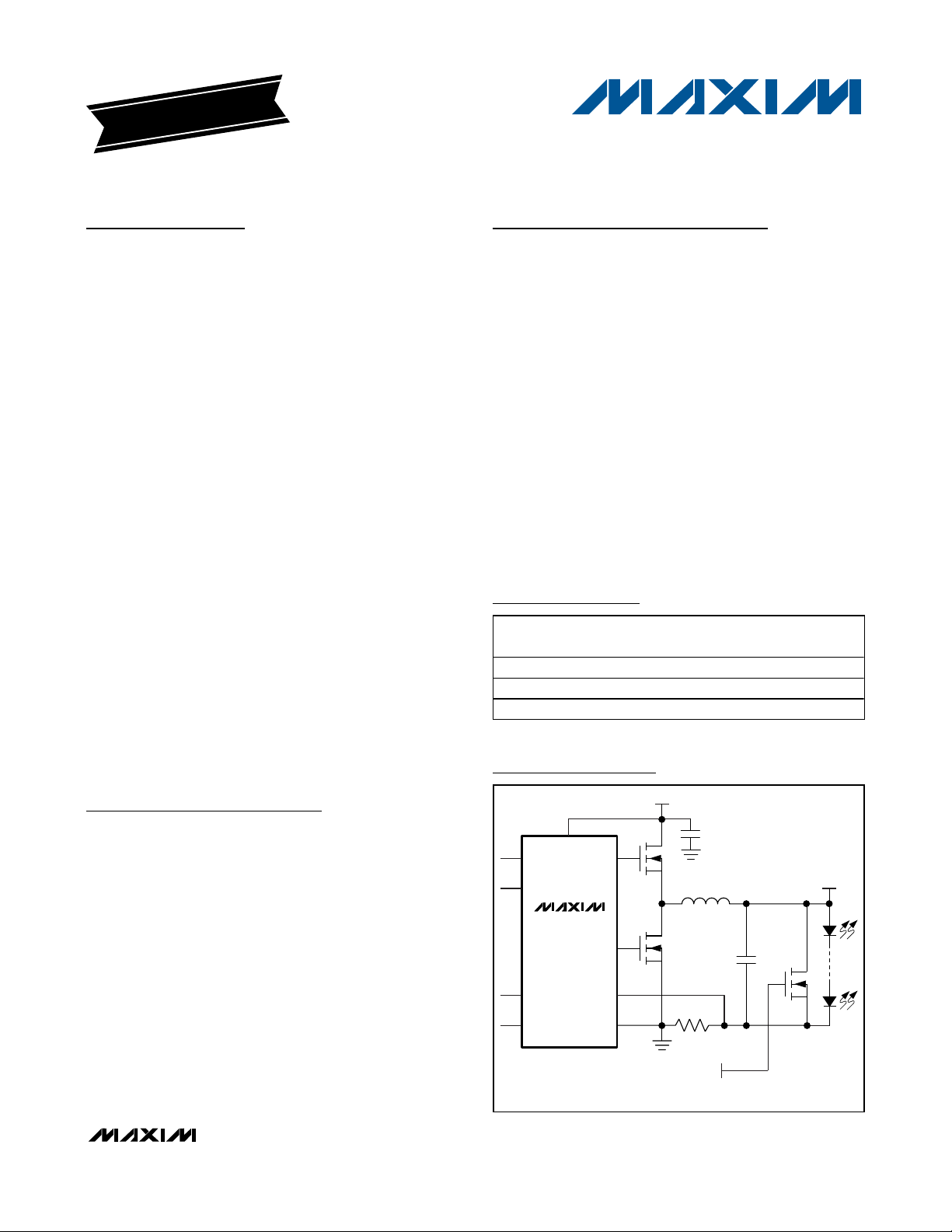
The MAX16821A/MAX16821B/MAX16821C feature a
clock output with 180° phase delay to control a second
out-of-phase LED driver to reduce input and output filter capacitor size and to minimize ripple currents. The
wide switching frequency range (125kHz to 1.5MHz)
allows the use of small inductors and capacitors.
Additional features include programmable overvoltage
protection and an output enable function.
Applications
Front Projectors/Rear Projection TVs
Portable and Pocket Projectors
Automotive Exterior Lighting
LCD TVs and Display Backlight
Automotive Emergency Lighting and Signage
Features
♦ Up to 30A Output Current
♦ True-Differential Remote Output Sensing
♦ Average Current-Mode Control
♦ 4.75V to 5.5V or 7V to 28V Input-Voltage Range
♦ 0.1V/0.03V LED Current-Sense Options Maximize
Efficiency (MAX16821B/MAX16821C)
♦ Thermal Shutdown
♦ Nonlatching Output Overvoltage Protection
♦ Low-Side Buck Mode with or without
Synchronous Rectification
♦ High-Side Buck and Low-Side Boost Mode with or
without Synchronous Rectification
♦ 125kHz to 1.5MHz Programmable/Synchronizable
Switching Frequency
♦ Integrated 4A Gate Drivers
♦ Clock Output for 180° Out-of-Phase Operation for
Second Driver
♦ -40°C to +125°C Operating Temperature Range
MAX16821A/MAX16821B/MAX16821C
High-Power Synchronous HBLED
Drivers with Rapid Current Pulsing
________________________________________________________________
Maxim Integrated Products
1
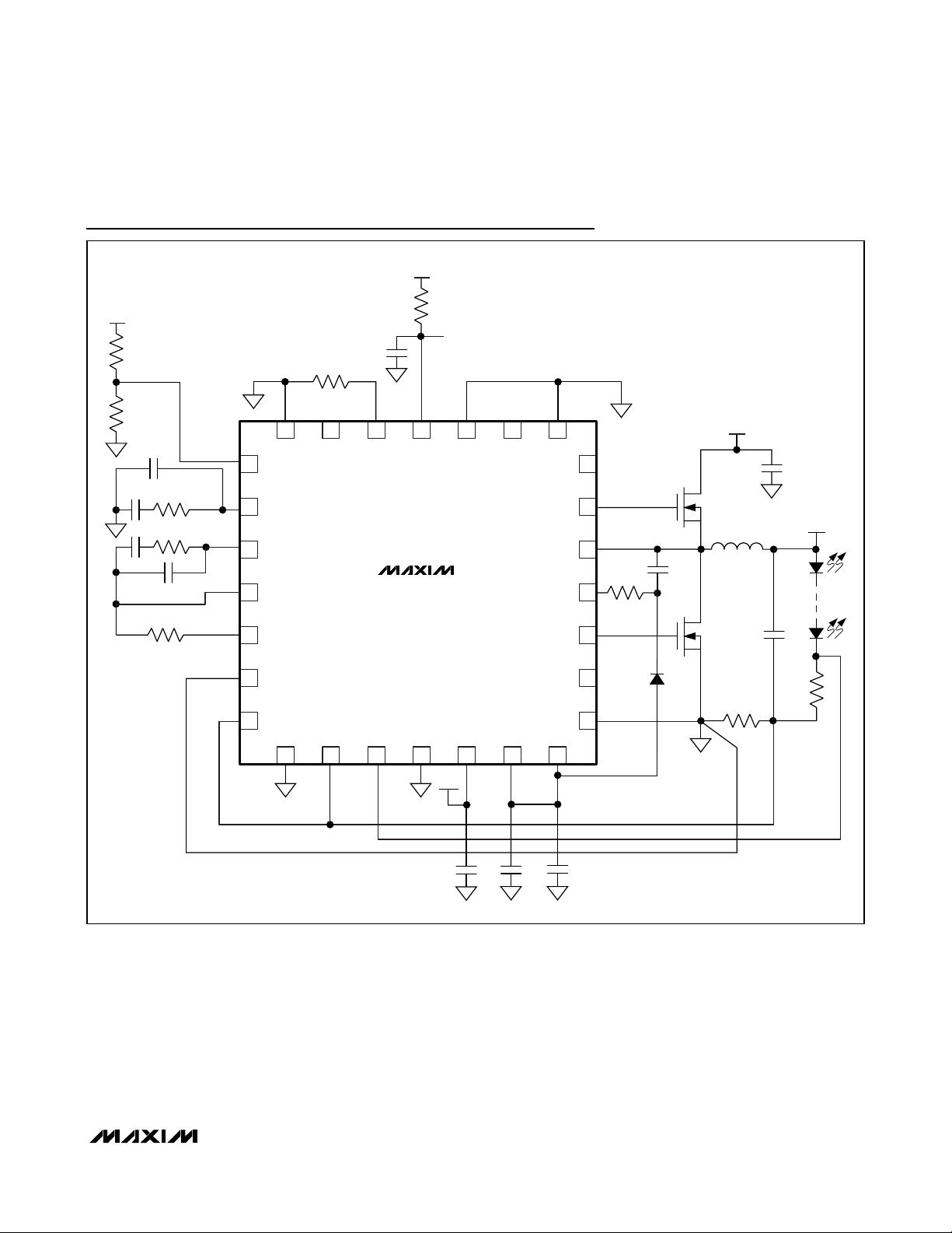
Simplified Diagram
19-0881; Rev 0; 7/07
For pricing, delivery, and ordering information, please contact Maxim Direct at 1-888-629-4642,
or visit Maxim’s website at www.maxim-ic.com.
EVALUATION KIT
AVAILABLE
Typical Operating Circuit and Selector Guide appear at end
of data sheet.
Ordering Information
+
Denotes a lead-free package.
*
EP = Exposed pad.
PART TEMP RANGE
MAX16821AATI+ -40°C to +125°C 28 TQFN-EP* T2855-8
MAX16821BATI+ -40°C to +125°C 28 TQFN-EP* T2855-8
MAX16821CATI+ -40°C to +125°C 28 TQFN-EP* T2855-8
PINPACKAGE
PKG
CODE
7V TO 28V
C1
V
L1
C2
Q3
R1
LED
EN
I.C.
OVI
CLP
IN
MAX16821
CSP
PGND
Q1
DH
Q2
DL
.
PULSE TRAIN
HIGH-FREQUENCY
NOTE: MAXIM PATENT-PENDING TOPOLOGY
MAX16821A/MAX16821B/MAX16821C
High-Power Synchronous HBLED
Drivers with Rapid Current Pulsing
2 _______________________________________________________________________________________
ABSOLUTE MAXIMUM RATINGS
ELECTRICAL CHARACTERISTICS
(VCC= 5V, VDD= VCC, TA= TJ= -40°C to +125°C, unless otherwise noted. Typical values are at TA= +25°C.) (Note 1)
Stresses beyond those listed under “Absolute Maximum Ratings” may cause permanent damage to the device. These are stress ratings only, and functional
operation of the device at these or any other conditions beyond those indicated in the operational sections of the specifications is not implied. Exposure to
absolute maximum rating conditions for extended periods may affect device reliability.
IN to SGND.............................................................-0.3V to +30V
BST to SGND..........................................................-0.3V to +35V
BST to LX..................................................................-0.3V to +6V
DH to LX...........................................-0.3V to (V
BST
- VLX) + 0.3V
DL to PGND................................................-0.3V to (V
DD
+ 0.3V)
V
CC
to SGND............................................................-0.3V to +6V
V
CC
, VDDto PGND ...................................................-0.3V to +6V
SGND to PGND .....................................................-0.3V to +0.3V
V
CC
Current ......................................................................300mA
All Other Pins to SGND...............................-0.3V to (V
CC
+ 0.3V)
Continuous Power Dissipation (T
A
= +70°C)
28-Pin TQFN 5mm x 5mm (derate 34.5mW/°C
above +70°C) ............................................................2758mW
Operating Temperature Range .........................-40°C to +125°C
Junction Temperature......................................................+150°C
Storage Temperature Range .............................-65°C to +150°C
Lead Temperature (soldering, 10s) .................................+300°C
PARAMETER SYMBOL CONDITIONS MIN TYP MAX UNITS
Input-Voltage Range V
Quiescent Supply Current I
LED CURRENT REGULATOR
Differential Set Value
(V
SENSE
+ to V
SENSE-
) (Note 2)
IN
Q
Soft-Start Time t
STARTUP/INTERNAL REGULATOR
V
U nd er vol tag e Lockout ( U V LO ) UVLO VCC rising 4.1 4.3 4.5 V
C C
UVLO Hysteresis VCC falling 200 mV
V
Output Voltage VIN = 7V to 28V, I
CC
MOSFET DRIVER
Output Driver Impedance Low or high output, I
Output Driver Source/Sink Current IDH, I
Nonoverlap Time t
SS
NO
Internal LDO on 7 28
Internal LDO off (V
VEN = VCC or SGND, no switching 2.7 5.5 mA
VIN = VCC = 4.75V to 5.5V, fSW = 500kHz
(MAX16821A)
VIN = 7V to 28V, fSW = 500kHz
(MAX16821A)
VIN = VCC = 4.75V to 5.5V, fSW = 500kHz
(MAX16821B)
VIN = 7V to 28V, fSW = 500kHz
(MAX16821B)
VIN = VCC = 4.75V to 5.5V, fSW = 500kHz
(MAX16821C)
V
= 7V to 28V, fSW = 500kHz
IN
(MAX16821C)
DL
C
= 5nF 35 ns
DH/DL
connected to VIN) 4.75 5.50
CC
= 0 to 60mA 4.85 5.10 5.30 V
SOURCE
SOURCE/SINK
= 20mA 1.1 3 Ω
0.594 0.600 0.606
0.594 0.600 0.606
0.098 0.100 0.102
0.098 0.100 0.102
0.028 0.030 0.032
0.028 0.030 0.032
1024
4A
V
V
Clock
Cycles
MAX16821A/MAX16821B/MAX16821C
High-Power Synchronous HBLED
Drivers with Rapid Current Pulsing
_______________________________________________________________________________________ 3
ELECTRICAL CHARACTERISTICS (continued)
(VCC= 5V, VDD= VCC, TA= TJ= -40°C to +125°C, unless otherwise noted. Typical values are at TA= +25°C.) (Note 1)
)
PARAMETER SYMBOL CONDITIONS MIN TYP MAX UNITS
OSCILLATOR
Switching Frequency Range 125 1500 kHz
RT = 500kΩ 120 125 130
SW
Switching Frequency Accuracy
CLKOUT Phase Shift with
Respect to DH (Rising Edges)
CLKOUT Phase Shift with
Respect to DL (Rising Edges)
CLKOUT Output-Voltage Low V
CLKOUT Output-Voltage High V
SYNC Input High Pulse Width t
SYNC Input Clock High Threshold V
SYNC Input Clock Low Threshold V
SYNC Pullup Current I
SYNC Power-Off Level V
INDUCTOR CURRENT LIMIT
Average Current-Limit Threshold V
Reverse Current-Limit Threshold V
Cycle-by-Cycle Current Limit CSP to CSN 60 mV
Cycle-by-Cycle Overload
CURRENT-SENSE AMPLIFIER
CSP to CSN Input Resistance R
Common-Mode Range V
Input Offset Voltage V
Amplifier Voltage Gain A
3dB Bandwidth f
CURRENT-ERROR AMPLIFIER (TRANSCONDUCTANCE AMPLIFIER)
Transconductance g
Open-Loop Gain A
OL
OH
SYNC
SYNCH
SYNCL
SYNC_OUTVRT/SYNC
SYNC_OFF
CL
CLR
CS
CMR(CS
OS(CS)
V(CS)
3dB
m
VL(CE)
RT = 120kΩ 495 521 547Switching Frequency f
RT = 39.9kΩ 1515 1620 1725
120kΩ < RT ≤ 500kΩ -5 +5
40kΩ ≤ R
f
SW
f
SW
I
SINK
I
SOURCE
CSP to CSN 26.4 27.5 30.0 mV
CSP to CSN -2.0 mV
V
CSP
VIN = 7V to 28V 0 5.5 V
≤ 120kΩ -8 +8
T
= 125kHz, MODE connected to SGND 180
= 125kHz, MODE connected to V
= 2mA 0.4 V
= 2mA 4.5 V
= 0V 250 500 µA
to V
= 75mV 260 ns
CSN
CC
200 ns
180
2V
0.4 V
0.4 V
4kΩ
0.1 mV
34.5 V/V
4 MHz
550 µS
50 dB
kHz
%
Degrees
MAX16821A/MAX16821B/MAX16821C
High-Power Synchronous HBLED
Drivers with Rapid Current Pulsing
4 _______________________________________________________________________________________
ELECTRICAL CHARACTERISTICS (continued)
(VCC= 5V, VDD= VCC, TA= TJ= -40°C to +125°C, unless otherwise noted. Typical values are at TA= +25°C.) (Note 1)
)
)
)
PARAMETER SYMBOL CONDITIONS MIN TYP MAX UNITS
LED CURRENT SIGNAL DIFFERENTIAL VOLTAGE AMPLIFIER (DIFF)
Common-Mode Voltage Range V
DIFF Output Voltage V
Input Offset Voltage V
SENSE+ to SENSE- Input
Resistance
OUTV AMPLIFIER
Gain-Bandwidth Product V
3dB Bandwidth V
Output Sink Current 30 µA
Output Source Current 80 µA
Maximum Load Capacitance 50 pF
OUTV to (CSP - CSN) Transfer
Function
Input Offset Voltage 1mV
VOLTAGE-ERROR AMPLIFIER (EAOUT)
Open-Loop Gain A
Unity-Gain Bandwidth f
EAN Input Bias Current I
Error Amplifier Output Clamping
Voltage
INPUTS (MODE AND OVI)
MODE Input-Voltage High 2V
MODE Input-Voltage Low 0.8 V
MODE Pulldown Current 456µA
OVI Trip Threshold OVP
OVI Hysteresis OVI
OVI Input Bias Current I
CMR(DIFF
CM
OS(DIFF
V(DIFF)
3dB
R
VS
VOLEA
GBW
B(EA)
V
CLAMP(EA
HYS
OVI
V
MAX16821A -3.7 +3.7
MAX16821B/MAX16821C -1.5 +1.5
MAX16821A 0.992 1 1.008
MAX16821B 5.9 6 6.1Amplifier Voltage Gain A
MAX16821C 18.5 20 21.5
MAX16821A, C
MAX16821B, C
MAX16821C, C
MAX16821A 50 100
MAX16821B 30 60
MAX16821C 10 20
4mV ≤ C
V
With respect to V
TH
V
= V
SENSE+
= 2V 4 MHz
OUTV
= 2V 1 MHz
OUTV
- CSN ≤ 32mV 132.5 135 137.7 V/V
SP
= 2V -0.2 +0.03 +0.2 µA
EAN
= 1V 0.2 µA
OVI
= 0V 0.6 V
SENSE-
= 20pF 1.7 MHz
DIFF
= 20pF 16003dB Bandwidth f
DIFF
= 20pF 550
DIFF
CM
0 1.0 V
mV
V/V
kHz
kΩ
70 dB
3 MHz
905 930 940 mV
1.244 1.276 1.308 V
200 mV
MAX16821A/MAX16821B/MAX16821C
High-Power Synchronous HBLED
Drivers with Rapid Current Pulsing
_______________________________________________________________________________________ 5
Note 1: All devices are 100% production tested at +25°C. Limits over temperature are guaranteed by design.
Note 2: Does not include an error due to finite error amplifier gain. See the
Voltage-Error Amplifier
section.
ELECTRICAL CHARACTERISTICS (continued)
(VCC= 5V, VDD= VCC, TA= TJ= -40°C to +125°C, unless otherwise noted. Typical values are at TA= +25°C.) (Note 1)
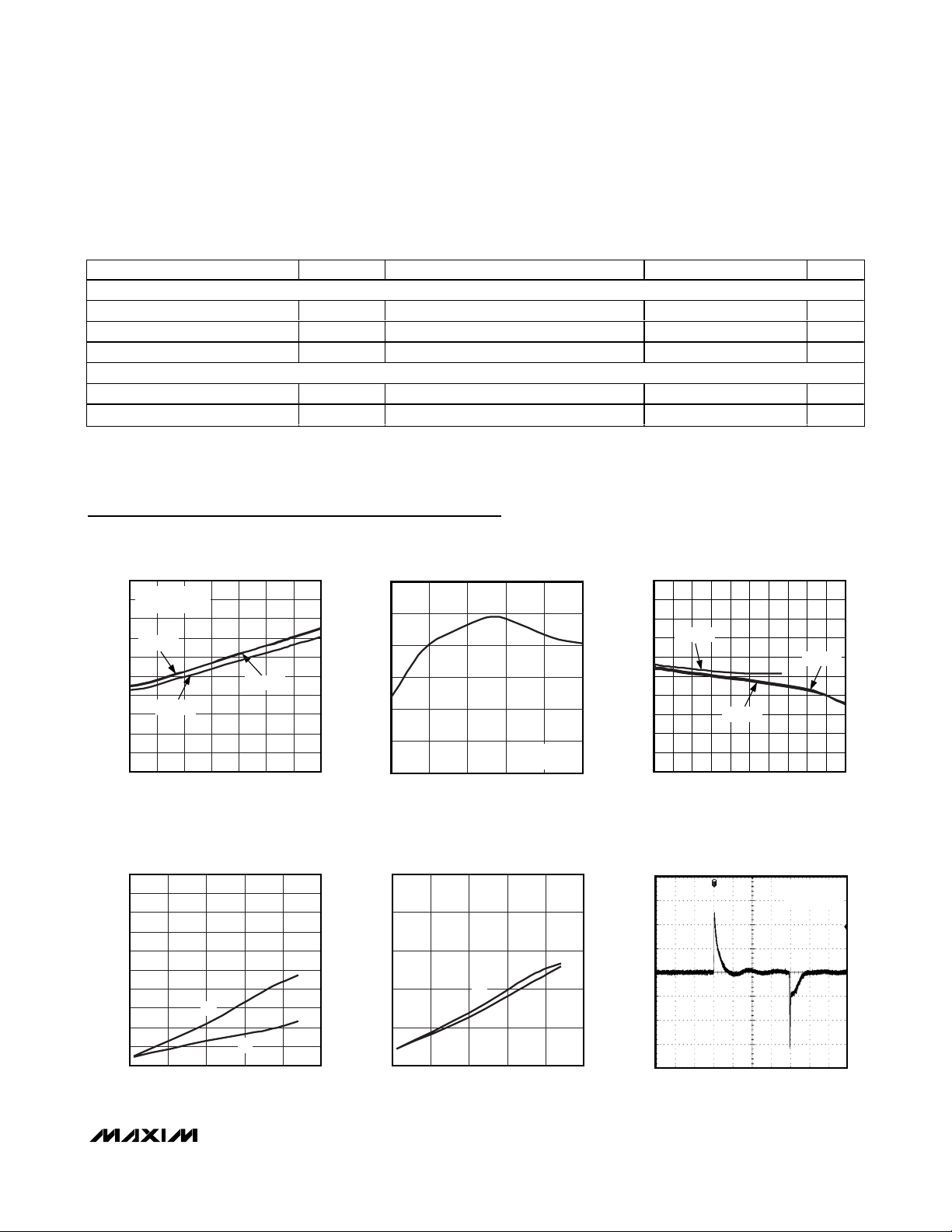
Typical Operating Characteristics
(VIN= 12V, VDD= V
CC
= 5V, TA= +25°C, unless otherwise noted.)
SUPPLY CURRENT (IQ) vs. FREQUENCY
MAX16821A toc01
FREQUENCY (kHz)
SUPPLY CURRENT (mA)
1300900 1100500 700300
1
2
3
4
5
6
7
8
9
10
0
100 1500
VIN = 24V
EXTERNAL CLOCK
NO DRIVER LOAD
VIN = 5V
VIN = 12V
SUPPLY CURRENT vs. TEMPERATURE
MAX16821A toc02
TEMPERATURE (°C)
SUPPLY CURRENT (mA)
603510-15
45
50
55
60
65
70
40
-40 85
VIN = 12V
C
DH/DL
= 22nF
VCC LOAD REGULATION vs. V
IN
MAX16821A toc03
VCC LOAD CURRENT (mA)
V
CC
(V)
13512090 10530 45 60 7515
4.6
4.7
4.8
4.9
5.0
5.1
5.2
5.3
5.4
5.5
4.5
0150
VIN = 24V
VIN = 7V
VIN = 12V
DRIVER RISE TIME
vs. DRIVER LOAD CAPACITANCE
MAX16821A toc04
LOAD CAPACITANCE (nF)
t
R
(ns)
2015510
20
40
60
80
100
120
140
160
180
200
0
025
DH
DL
DRIVER FALL TIME
vs. DRIVER LOAD CAPACITANCE
MAX16821A toc05
LOAD CAPACITANCE (nF)
f
F
(ns)
2015510
20
40
60
80
100
0
025
DH
DL
HIGH-SIDE DRIVER (DH) SINK
AND SOURCE CURRENT
MAX16821A toc06
2A/div
100ns/div
C
LOAD
= 22nF
V
IN
= 12V
PARAMETER SYMBOL CONDITIONS MIN TYP MAX UNITS
ENABLE INPUT (EN)
EN Input-Voltage High EN rising 2.437 2.5 2.562 V
EN Input Hysteresis 0.28 V
EN Pullup Current I
EN
13.5 15 16.5 µA
THERMAL SHUTDOWN
Thermal Shutdown 165 °C
Thermal-Shutdown Hysteresis 20 °C
MAX16821A/MAX16821B/MAX16821C
High-Power Synchronous HBLED
Drivers with Rapid Current Pulsing
6 _______________________________________________________________________________________
Typical Operating Characteristics (continued)
(VIN= 12V, VDD= V
CC
= 5V, TA= +25°C, unless otherwise noted.)
LOW-SIDE DRIVER (DL) SINK
AND SOURCE CURRENT
C
= 22nF
LOAD
= 12V
V
IN
100ns/div
LOW-SIDE DRIVER (DL) RISE TIME
C
= 22nF
LOAD
= 12V
V
IN
MAX16821A toc07
MAX16821A toc10
3A/div
2V/div
HIGH-SIDE DRIVER (DH) RISE TIME
VIN = 12V
DH RISING
40ns/div
LOW-SIDE DRIVER (DL) FALL TIME
MAX16821A toc08
C
LOAD
= 12V
V
IN
MAX16821A toc11
= 22nF
2V/div
2V/div
10,000
(kHz)
1000
SW
f
HIGH-SIDE DRIVER (DH) FALL TIME
C
= 22nF
LOAD
= 12V
V
IN
40ns/div
FREQUENCY vs. R
VIN = 12V
MAX16821A toc09
T
2V/div
MAX16821A toc12
40ns/div
40ns/div
100
30 550
FREQUENCY vs. TEMPERATURE
260
VIN = 12V
258
256
254
252
(kHz)
250
SW
f
248
246
244
242
240
035
TEMPERATURE (°C)
3020 2551015
SYNC, CLKOUT, AND DH WAVEFORMS
MAX16821A toc13
1μs/div
MAX16821A toc14
MODE = SGND
RT/SYNC
5V/div
0V
CLKOUT
5V/div
0V
DH
5V/div
0V
SYNC, CLKOUT, AND DL WAVEFORMS
190
230 270 310
RT (kΩ)
1μs/div
430 470 510350 39 070 110 150
MODE = V
MAX16821A toc15
CC
RT/SYNC
5V/div
0V
CLKOUT
5V/div
0V
DL
5V/div
0V
MAX16821A/MAX16821B/MAX16821C
High-Power Synchronous HBLED
Drivers with Rapid Current Pulsing
_______________________________________________________________________________________ 7
Pin Description
PIN NAME FUNCTION
1 PGND Power-Supply Ground
2, 7 N.C. No Connection. Not internally connected.
3 DL Low-Side Gate-Driver Output
4 BST
5 LX High-Side MOSFET Source Connection
6 DH High-Side Gate-Driver Output
8, 22, 25 SGND
9 CLKOUT
10 MODE
11 EN
12 RT/SYNC
13 OUTV
14 I.C. Internally Connected. Connect to SGND for proper operation.
15 OVI
16 CLP Current-Error-Amplifier Output. Compensate the current loop by connecting an RC network to ground.
17 EAOUT Voltage-Error-Amplifier Output. Connect EAOUT to the external gain-setting network.
18 EAN Voltage-Error-Amplifier Inverting Input
19 DIFF
20 CSN
21 CSP
23 SENSE-
24 SENSE+
26 IN Supply Voltage Input. Connect IN to VCC, for a 4.75V to 5.5V input supply range.
27 V
28 V
—EP
Boost-Flying Capacitor Connection. Reservoir capacitor connection for the high-side MOSFET driver
supply. Connect a ceramic capacitor between BST and LX.
Signal Ground. SGND is the ground connection for the internal control circuitry. Connect SGND and PGND
together at one point near the IC.
Oscillator Output. If MODE is low, the rising edge of CLKOUT phase shifts from the rising edge of DH by
180°. If MODE is high, the rising edge of CLKOUT phase shifts from the rising edge of DL by 180°.
Buck/Boost Mode Selection Input. Drive MODE low for low-side buck mode operation. Drive MODE high for
boost or high-side buck mode operation. MODE has an internal 5µA pulldown current to ground.
Output Enable. Drives EN high or leave unconnected for normal operation. Drive EN low to shut down the
power drivers. EN has an internal 15µA pullup current.
Switching Frequency Programming. Connect a resistor from RT/SYNC to SGND to set the internal oscillator
frequency. Drive RT/SYNC to synchronize the switching frequency with an external clock.
Inductor Current-Sense Output. OUTV is an amplifier output voltage proportional to the inductor current.
The voltage at OUTV = 135 x (V
Overvoltage Protection. When OVI exceeds the programmed output voltage by 12.7%, the low-side and
the high-side drivers are turned off. When OVI falls 20% below the programmed output voltage, the drivers
are turned on after power-on reset and soft-start cycles are completed.
Differential Remote-Sense Amplifier Output. DIFF is the output of a precision amplifier with SENSE+ and
SENSE- as inputs.
Current-Sense Differential Amplifier Negative Input. The differential voltage between CSN and CSP is
amplified internally by the current-sense amplifier (Gain = 34.5) to measure the inductor current.
Current-Sense Differential Amplifier Positive Input. The differential voltage between CSP and CSN is
amplified internally by the current-sense amplifier (Gain = 34.5) to measure the inductor current.
Differential LED Current-Sensing Negative Input. Connect SENSE- to the negative side of the LED currentsense resistor or to the negative feedback point.
Differential LED Current-Sensing Positive Input. Connect SENSE+ to the positive side of the LED currentsense resistor, or to the positive feedback point.
Internal +5V Regulator Output. VCC is derived from VIN. Bypass VCC to SGND with 4.7µF and 0.1µF
CC
ceramic capacitors.
Low-Side Driver Supply Voltage
DD
Exposed Pad. EP is internally connected to SGND. Connect EP to a large-area ground plane for effective
power dissipation. Connect EP to SGND. Do not use as a ground connection.
CSP
- V
CSN
).

MAX16821A/MAX16821B/MAX16821C
High-Power Synchronous HBLED
Drivers with Rapid Current Pulsing
8 _______________________________________________________________________________________
Detailed Description
The MAX16821A/MAX16821B/MAX16821C are high-performance average current-mode PWM controllers for
high-power and high-brightness LEDs (HBLEDs). The
average current-mode control technique offers inherently
stable operation, reduces component derating and size
by accurately controlling the inductor current. The
devices achieve high efficiency at high currents (up to
30A) with a minimum number of external components. A
logic input (MODE) allows the LED driver to switch
between buck and boost modes of operation.
The MAX16821A/MAX16821B/MAX16821C feature a
CLKOUT output 180° out-of-phase with respect to either
the high-side or low-side driver, depending on MODE’s
logic level. CLKOUT provides the drive for a second
out-of-phase LED driver for applications requiring
reduced input capacitor ripple current while operating
another LED driver.
The MAX16821A/MAX16821B/MAX16821C consist of
an inner average current regulation loop controlled by
an outer loop. The combined action of the inner current
loop and outer voltage loop corrects the LED current
errors by adjusting the inductor current resulting in a
tightly regulated LED current. The differential amplifier
(SENSE+ and SENSE- inputs) senses the LED current
using a resistor in series with the LEDs and produces
an amplified version of the sense voltage at DIFF. The
resulting amplified sensed voltage is compared against
an internal 0.6V reference at the error amplifier input.
Input Voltage
The MAX16821A/MAX16821B/MAX16821C operate
with a 4.75V to 5.5V input supply range when the internal LDO is disabled (V
CC
connected to IN) or a 7V to
28V input supply range when the internal LDO is
enabled. For a 7V to 28V input voltage range, the internal LDO provides a regulated 5V output with 60mA of
sourcing capability. Bypass V
CC
to SGND with 4.7µF
and 0.1µF low-ESR ceramic capacitors.
The MAX16821A/MAX16821B/MAX16821C’s V
DD
input
provides supply voltage for the low-side and the highside MOSFET drivers. Connect V
DD
to V
CC
using an
R-C filter to isolate the analog circuits from the MOSFET
drivers. The internal LDO powers up the MAX16821A/
MAX16821B/MAX16821C. For applications utilizing a
5V input voltage, disable the internal LDO by connecting IN and VCCtogether. The 5V power source must be
in the 4.75V to 5.5V range of for proper operation of the
MAX16821A/MAX16821B/MAX16821C.
Undervoltage Lockout (UVLO)
The MAX16821A/MAX16821B/MAX16821C include
UVLO and a 2048 clock-cycle power-on-reset circuit.
The UVLO rising threshold is set to 4.3V with 200mV
hysteresis. Hysteresis at UVLO eliminates chattering
during startup. Most of the internal circuitry, including
the oscillator, turns on when the input voltage reaches
4V. The MAX16821A/MAX16821B/MAX16821C draw up
to 3.5mA of quiescent current before the input voltage
reaches the UVLO threshold.
Soft-Start
The MAX16821A/MAX16821B/MAX16821C include an
internal soft-start for a glitch-free rise of the output voltage. After 2048 power-on-reset clock cycles, a 0.6V
reference voltage connected to the positive input of the
internal error amplifier ramps up to its final value after
1024 clock cycles. Soft-start reduces inrush current
and stress on system components. During soft-start,
the LED current will ramp monotonically towards its
final value.
Internal Oscillator
The internal oscillator generates a clock with the frequency inversely proportional to the value of R
T
(see
the
Typical Operating Circuit
). The oscillator frequency
is adjustable from 125kHz to 1.5MHz range using a single resistor connected from RT/SYNC to SGND. The
frequency accuracy avoids the overdesign, size, and
cost of passive filter components like inductors and
capacitors. Use the following equation to calculate the
oscillator frequency:
For 120kΩ≤RT≤ 500kΩ:
For 40kΩ≤R
T
≤ 120kΩ:
The oscillator also generates a 2V
P-P
ramp signal for
the PWM comparator and a 180° out-of-phase clock
signal at CLKOUT to drive a second out-of-phase LED
current regulator.
.
f
SW
f
SW
625 10
640 10
.
10
x
R
x
R
()=
T
T
Hz
10
()=
Hz
MAX16821A/MAX16821B/MAX16821C
High-Power Synchronous HBLED
Drivers with Rapid Current Pulsing
_______________________________________________________________________________________ 9
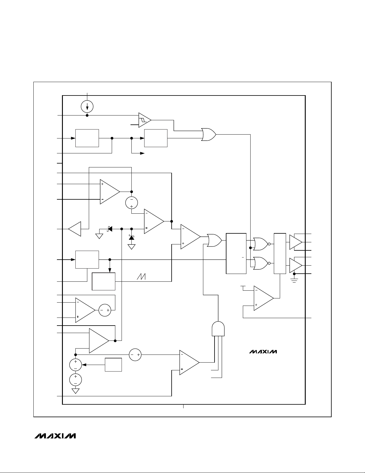
Figure 1. Internal Block Diagram
V
I.C.
CLP
CSP
CSN
OUTV
RT/SYNC
CLKOUT
V
CC
EN
0.5 x V
CC
UVLO
POR
TEMP SEN
TO INTERNAL CIRCUIT
g
m
V
HIGH
CLAMP
2 x f
S
PWM
COMPARATOR
S
Q
RQ
V
TH
MUX
BST
DH
LX
V
DD
DL
PGND
= 4
A
V
OSCILLATOR
+5V LDO
AV = 34.5
V
CLAMP
CLK
RAMP
GENERATOR
LOW
V
CM
IN
CC
DIFF
SENSE-
SENSE+
EAOUT
EAN
OVI
DIFF
AMP
ERROR
AMP
V
= 0.6V
REF
V
CM
V
CM
MODE
OVP
COMPARATOR
SGND
ENABLE
UVLO
MAX16821A
MAX16821B
MAX16821C
SOFTSTART
0.12 x V
REF

MAX16821A/MAX16821B/MAX16821C
High-Power Synchronous HBLED
Drivers with Rapid Current Pulsing
10 ______________________________________________________________________________________
Synchronization
The MAX16821A/MAX16821B/MAX16821C synchronize
to an external clock connected to RT/SYNC. The application of an external clock at RT/SYNC disables the
internal oscillator. Once the MAX16821A/MAX16821B/
MAX16821C are synchronized to an external clock, the
external clock cannot be removed if reliable operation
is to be maintained.
Control Loop
The MAX16821A/MAX16821B/MAX16821C use an
average current-mode control scheme to regulate the
output current (Figure 2). The main control loop consists of an inner current regulation loop for controlling
the inductor current and an outer current regulation
loop for regulating the LED current. The inner current
regulation loop absorbs the double pole of the inductor
and output capacitor combination reducing the order of
the outer current regulation loop to that of a single-pole
system. The inner current regulation loop consists of a
current-sense resistor (RS), a current-sense amplifier
(CSA), a current-error amplifier (CEA), an oscillator providing the carrier ramp, and a PWM comparator
(CPWM) (Figure 2). The MAX16821A/MAX16821B/
MAX16821C outer LED-current control loop consists of
a differential amplifier (DIFF), a reference voltage, and
a voltage-error amplifier (VEA).
Inductor Current-Sense Amplifier
The differential current-sense amplifier (CSA) provides a
34.5V/V DC gain. The typical input offset voltage of the
current-sense amplifier is 0.1mV with a 0 to 5.5V commonmode voltage range (V
IN
= 7V to 28V). The current-sense
amplifier senses the voltage across RS. The maximum
common-mode voltage is 3.2V when V
IN
= 5V.
Inductor Peak-Current Comparator
The peak-current comparator provides a path for fast
cycle-by-cycle current limit during extreme fault conditions, such as an inductor malfunction (Figure 3). Note
the average current-limit threshold of 27.5mV still limits
the output current during short-circuit conditions. To
prevent inductor saturation, select an inductor with a
saturation current specification greater than the average current limit. The 60mV threshold for triggering the
peak-current limit is twice the full-scale average current-limit voltage threshold. The peak-current comparator has only a 260ns delay.
Figure 2. MAX16821A/MAX16821B/MAX16821C Control Loop
C
R
IN
F
R
F
C
CP
R
CF
C
CZ
DIFF
EAN EAOUT CSN CSP CLP
CA
SENSE+
SENSE-
DIFF
V
REF
VEA
CEA
CPWM
MODE = SGND
DRIVER
V
IN
L
R
S
LED
STRING
C
OUT
R
LS

MAX16821A/MAX16821B/MAX16821C
High-Power Synchronous HBLED
Drivers with Rapid Current Pulsing
______________________________________________________________________________________ 11
Current-Error Amplifier
The MAX16821A/MAX16821B/MAX16821C include a
transconductance current-error amplifier with a typical
g
m
of 550µS and 320µA output sink and source capability. The current-error amplifier output (CLP) is connected to the inverting input of the PWM comparator.
CLP is also externally accessible to provide frequency
compensation for the inner current regulation loop
(Figure 2). Compensate CEA so the inductor current
negative slope, which becomes the positive slope to
the inverting input of the PWM comparator, is less than
the slope of the internally generated voltage ramp (see
the
Compensation
section). In applications without synchronous rectification, the LED driver can be turned off
and on instantaneously by shorting or opening the CLP
to ground.
PWM Comparator and R-S Flip-Flop
An internal PWM comparator sets the duty cycle by
comparing the output of the current-error amplifier to a
2V
P-P
ramp signal. At the start of each clock cycle, an
R-S flip-flop resets and the high-side driver (DH) turns
on if MODE is connected to SGND, and DL turns on if
MODE is connected to V
CC
. The comparator sets the
flip-flop as soon as the ramp signal exceeds the CLP
voltage, thus terminating the ON cycle. See Figure 3.
Differential Amplifier
The differential amplifier (DIFF) allows LED current sensing (Figure 2). It provides true-differential LED current
sensing, and amplifies the sense voltage by a factor of 1
(MAX16821A), 6 (MAX16821B), and 20 (MAX16821C),
while rejecting common-mode voltage errors. The VEA
provides the difference between the differential amplifier
output (DIFF) and the desired LED current-sense voltage. The differential amplifier has a bandwidth of 1.7MHz
(MAX16821A), 1.6MHz (MAX16821B), and 550kHz
(MAX16821C). The difference between SENSE+ and
SENSE- is regulated to +0.6V (MAX16821A), +0.1V
(MAX16821B), or +0.03V (MAX16821C).
Figure 3. MAX16821A/MAX16821B/MAX16821C Phase Circuit
60mV
PEAK-CURRENT
COMPARATOR
CLP
= 34.5
A
CSP
CSN
IN
RAMP
CLK
SHDN
V
gm = 550μS
PWM
COMPARATOR
MODE = GND
SQ
RQ
BST
DH
LX
V
DD
DL
PGND

MAX16821A/MAX16821B/MAX16821C
High-Power Synchronous HBLED
Drivers with Rapid Current Pulsing
12 ______________________________________________________________________________________
Voltage-Error Amplifier (VEA)
The VEA sets the gain of the voltage control loop, and
determines the error between the differential amplifier
output and the internal reference voltage. The VEA output clamps to 0.93V relative to the internal commonmode voltage, V
CM
(+0.6V), limiting the average maximum current. The maximum average current-limit
threshold is equal to the maximum clamp voltage of the
VEA divided by the gain (34.5) of the current-sense
amplifier. This results in accurate settings for the average maximum current.
MOSFET Gate Drivers
The high-side (DH) and low-side (DL) drivers drive the
gates of external n-channel MOSFETs. The drivers’ 4A
peak sink- and source-current capability provides
ample drive for the fast rise and fall times of the switching MOSFETs. Faster rise and fall times result in
reduced cross-conduction losses. Size the high-side
and low-side MOSFETs to handle the peak and RMS
currents during overload conditions. The driver block
also includes a logic circuit that provides an adaptive
nonoverlap time to prevent shoot-through currents during transition. The typical nonoverlap time is 35ns
between the high-side and low-side MOSFETs.
BST
The MAX16821A/MAX16821B/MAX16821C provide
power to the low-side and high-side MOSFET drivers
through VDD. A bootstrap capacitor from BST to LX provides the additional boost voltage necessary for the
high-side driver. V
DD
supplies power internally to the
low-side driver. Connect a 0.47µF low-ESR ceramic
capacitor between BST and LX and a Schottky diode
from BST to V
DD
.
Protection
The MAX16821A/MAX16821B/MAX16821C include output overvoltage protection (OVP). During fault conditions when the load goes to high impedance (output
opens), the controller attempts to maintain LED current.
The OVP disables the MAX16821A/MAX16821B/
MAX16821C whenever the output voltage exceeds the
OVP threshold, protecting the external circuits from
undesirable voltages.
Current Limit
The error amplifier (VEA) output is clamped between
-0.050V and +0.93V with respect to common-mode
voltage (V
CM
). Average current-mode control limits the
average current sourced by the converter during a fault
condition. When a fault condition occurs, the VEA output clamps to +0.93V with respect to the commonmode voltage (0.6V) to limit the maximum current
sourced by the converter to I
LIMIT
= 0.0275 / RS.
Overvoltage Protection
The OVP comparator compares the OVI input to the
overvoltage threshold. The overvoltage threshold is typically 1.127 times the internal 0.6V reference voltage
plus V
CM
(0.6V). A detected overvoltage event trips the
comparator output turning off both high-side and lowside MOSFETs. Add an RC delay to reduce the sensitivity of the overvoltage circuit and avoid unnecessary
tripping of the converter (Figure 4). After the OVI voltage falls below 1.076V (typ.), high-side and low-side
drivers turn on only after a 2048 clock-cycle POR and a
1024 clock-cycle soft-start have elapsed. Disable the
overvoltage function by connecting OVI to SGND.
Figure 4. Overvoltage Protection Input Delay
MAX16821A
MAX16821B
MAX16821C
OVI
DIFF
EAN
EAOUT
RB
C
OVI
RA
R
F
V
OUT
R
IN

MAX16821A/MAX16821B/MAX16821C
High-Power Synchronous HBLED
Drivers with Rapid Current Pulsing
______________________________________________________________________________________ 13
Applications Information
Boost LED Driver
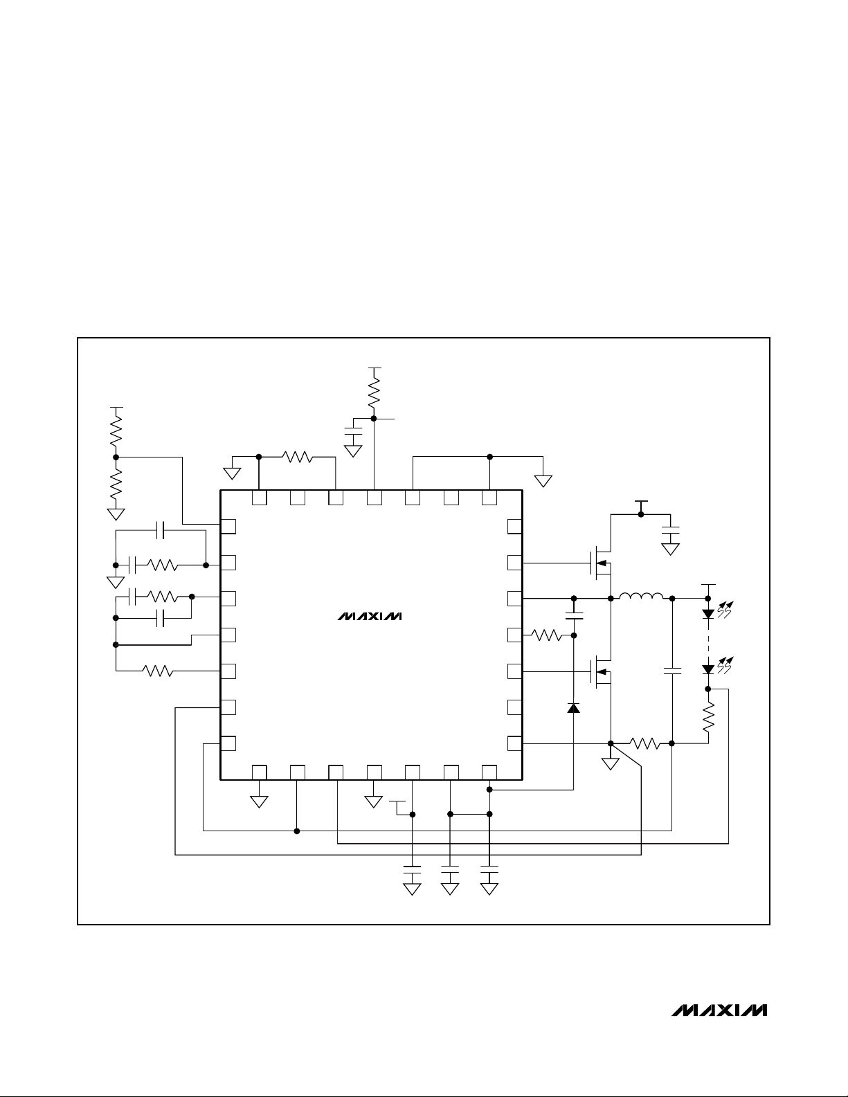
Figure 5 shows the MAX16821A/MAX16821B/MAX16821C
configured as a synchronous boost converter with
MODE connected to V
CC
. During the on-time, the input
voltage charges the inductor. During the off-time, the
inductor discharges to the output. The output voltage
cannot go below the input voltage in this configuration.
Resistor R1 senses the inductor current and resistor R2
senses the LED current. The outer LED current regulation loop programs the average current in the inductor,
thus achieving tight LED current regulation.
Figure 5. Synchronous Boost LED Driver (Output Voltage Not to Exceed 28V)
V
LED
R9
R10
C11
C10
R8
R7
C9
C8
R5
R4
C3
R3
12
1314
I.C. OUTV RT/SYNC EN MODE CLKOUT SGND
15
OVI
16
CLP
EAOUT
17
EAN
18
MAX16821A
MAX16821B
MAX16821C
19
DIFF
V
CC
11
ON/OFF
V
IN
7V TO 28V
9
10
8
N.C.
BST
DL
L1
7
DH
6
5
LX
4
3
Q2
C4
R5
C2
V
Q1
C1
R2
LED
LED
STRING
20
CSN
CSP
21
SGND SENSE- SENSE+ SGND IN V
22 23
24 25 26
V
IN
C7
CC
27 28
C6 C5
N.C.
PGND
V
DD
2
1
D1
R1

MAX16821A/MAX16821B/MAX16821C
High-Power Synchronous HBLED
Drivers with Rapid Current Pulsing
14 ______________________________________________________________________________________
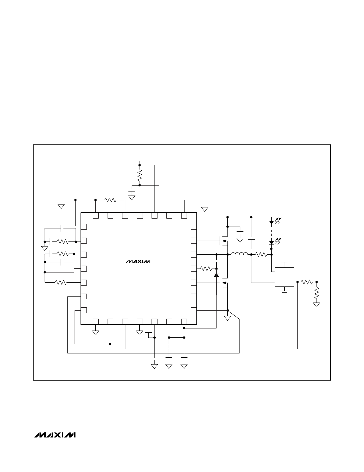
Input-Referenced Buck-Boost LED Driver
The circuit in Figure 6 shows a step-up/step-down regulator. It is similar to the boost converter in Figure 5 in
that the inductor is connected to the input and the
MOSFET is essentially connected to ground. However,
rather than going from the output to ground, the LEDs
span from the output to the input. This effectively
removes the boost-only restriction of the regulator in
Figure 5, allowing the voltage across the LED to be
greater or less than the input voltage. LED currentsensing is not ground-referenced, so a high-side current-sense amplifier is used to measure current.
Figure 6. Typical Application Circuit for an Input-Referred Buck-Boost LED Driver (7V to 28V Input)
V
CC
V
LED
R8
R9
C10
C11
R7
R6
C9
C8
R5
15
OVI
16
CLP
EAOUT
17
EAN
18
19
DIFF
R3
1314
I.C. OUTV RT/SYNC EN MODE CLKOUT SGND
R4
C3
12
MAX16821A
MAX16821B
MAX16821C
11
ON/OFF
9
10
8
N.C.
BST
7
DH
6
5
LX
4
3
DL
L1
V
IN
7V TO 28V
D1
Q1
C1
R2
C2
C2
RS+
RS-
LED
STRING
1 TO 6
LEDS
V
LED
V
CC
OUT
20
CSN
CSP
21
SGND SENSE- SENSE+ SGND IN V
22 23
24 25 26
V
IN
C7
CC
27 28
C6 C5
N.C.
PGND
V
DD
2
1
R1

SEPIC LED Driver
Figure 7 shows the MAX16821A/MAX16821B/
MAX16821C configured as a SEPIC LED driver. While
buck topologies produce an output always lower than
the input, and boost topologies produce an output
always greater than the input, a SEPIC topology allows
the output voltage to be greater than, equal to, or less
than the input. In a SEPIC topology, the voltage across
C3 is the same as the input voltage, and L1 and L2 have
the same inductance. Therefore, when Q1 turns on (ontime), the currents in both inductors (L1 and L2) ramp
up at the same rate. The output capacitor supports the
output voltage during this time. When Q1 turns off (offtime), L1 current recharges C3 and combines with L2 to
provide current to recharge C1 and supplies the load
current. Since the voltage waveform across L1 and L2
are exactly the same, it is possible to wind both inductors on the same core (a coupled inductor). Although
voltages on L1 and L2 are the same, RMS currents can
be quite different so the windings may require a different gauge wire. Because of the dual inductors and segmented energy transfer, the efficiency of a SEPIC
converter is lower than the standard buck or boost configurations. As in the boost driver, the current-sense
resistor connects to ground, allowing the output voltage
of the LED driver to exceed the rated maximum voltage
of the MAX16821A/MAX16821B/MAX16821C.
MAX16821A/MAX16821B/MAX16821C
High-Power Synchronous HBLED
Drivers with Rapid Current Pulsing
______________________________________________________________________________________ 15
Figure 7. Typical Application Circuit for a SEPIC LED Driver
V
CC
C2
12
MAX16821A
MAX16821B
MAX16821C
R4
11
V
LED
R8
R9
C10
C9
R7
R6
C8
C7
R5
15
OVI
16
CLP
EAOUT
17
EAN
18
19
DIFF
R3
1314
I.C. OUTV RT/SYNC EN MODE CLKOUT SGND
ON/OFF
9
10
8
N.C.
BST
7
DH
6
5
LX
4
3
DL
L1
V
IN
7V TO 28V
C3
Q1
L2
V
D1
LED
C1
R2
LED
STRING
20
CSN
CSP
21
SGND SENSE- SENSE+ SGND IN V
22 23
24 25 26
2
N.C.
PGND
1
V
CC
DD
27 28
V
IN
C5 C4
C6
R1
MAX16821A/MAX16821B/MAX16821C
Low-Side Buck Driver
with Synchronous Rectification
In Figure 8, the input voltage goes from 7V to 28V and,
because of the ground-based current-sense resistor,
the output voltage can be as high as the input. The synchronous MOSFET keeps the power dissipation to a
minimum, especially when the input voltage is large
compared to the voltage on the LED string. For the
inner average current-loop inductor, current is sensed
by resistor R1. To regulate the LED current, R2 creates
a voltage that the differential amplifier compares to
0.6V. Capacitor C1 is small and helps reduce the ripple
current in the LEDs. Omit C1 in cases where the LEDs
can tolerate a higher ripple current. The average currentmode control scheme converts the input voltage to a
current source feeding the LED string.
High-Power Synchronous HBLED
Drivers with Rapid Current Pulsing
16 ______________________________________________________________________________________
Figure 8. Application Circuit for a Low-Side Buck LED Driver
V
CC
V
LED
R9
R10
C10
C9
C11
C8
R6
15
OVI
R9
R7
16
CLP
EAOUT
17
EAN
18
19
DIFF
R3
1314
I.C. OUTV RT/SYNC EN MODE CLKOUT SGND
R4
C3
12
MAX16821A
MAX16821B
MAX16821C
11
ON/OFF
V
IN
9
10
8
N.C.
LX
BST
DL
7
DH
6
5
R5
4
3
7V TO 28V
C2
Q1
L1
C4
Q2
C1
V
LED
LED
STRING
20
CSN
CSP
21
SGND SENSE- SENSE+ SGND IN V
22 23
24 25 26
V
C7
CC
27 28
IN
C6 C5
N.C.
PGND
V
DD
2
1
D2
R2
R1
High-Side Buck Driver
with Synchronous Rectification
In Figure 9, the input voltage goes from 7V to 28V, the LED
load is connected from the positive side to the currentsense resistor (R1) in series with the inductor, and MODE
is connected to VCC. For the inner average current-loop
inductor, current is sensed by resistor R1 and is then
transferred to the low side by the high-side current-sense
amplifier, U2. The voltage appearing across resistor R11
becomes the average inductor current-sense voltage for
the inner average current loop. To regulate the LED
current, R2 creates a voltage that the differential amplifier compares to its internal reference. Capacitor C1 is
small and is added to reduce the ripple current in the
LEDs. In cases where the LEDs can tolerate a higher
ripple current, capacitor C1 can be omitted.
MAX16821A/MAX16821B/MAX16821C
High-Power Synchronous HBLED
Drivers with Rapid Current Pulsing
______________________________________________________________________________________ 17
Figure 9. Application Circuit for a High-Side Buck LED Driver
V
CC
R4
ON/OFF
9
10
C10
C3
R3
12
1314
C11
R8
R7
C9
C8
R6
I.C. OUTV RT/SYNC EN MODE CLKOUT SGND
15
OVI
I.C.
16
CLP
EAOUT
17
EAN
18
19
DIFF
11
MAX16821A
MAX16821B
MAX16821C
V
IN
8
N.C.
BST
7
DH
6
5
LX
4
3
DL
7V TO 28V
C2
Q1
L1
C4
R5
D1
Q2
LED
STRING
C1
RS+
RS-
V
CC
U2
OUT
R2
R1
20
CSN
CSP
21
SGND SENSE- SENSE+ SGND IN V
22 23
24 25 26
V
IN
C7
C6 C5
CCVDD
27 28
N.C.
PGND
2
1
R11

MAX16821A/MAX16821B/MAX16821C
Inductor Selection
The switching frequency, peak inductor current, and
allowable ripple at the output determine the value and
size of the inductor. Selecting higher switching frequencies reduces inductance requirements, but at the cost
of efficiency. The charge/discharge cycle of the gate
and drain capacitance in the switching MOSFETs create switching losses worsening at higher input voltages, since switching losses are proportional to the
square of the input voltage. The MAX16821A/
MAX16821B/MAX16821C operate up to 1.5MHz.
Choose inductors from the standard high-current, surface-mount inductor series available from various manufacturers. Particular applications may require
custom-made inductors. Use high-frequency core material for custom inductors. High ΔI
L
causes large peak-topeak flux excursion increasing the core losses at higher
frequencies. The high-frequency operation coupled with
high ΔILreduces the required minimum inductance and
makes the use of planar inductors possible.
The following discussion is for buck or continuous
boost-mode topologies. Discontinuous boost, buckboost, and SEPIC topologies are quite different in
regards to component selection. Use the following
equations to determine the minimum inductance value:
Buck regulators:
Boost regulators:
where V
LED
is the total voltage across the LED string.
The average current-mode control feature of the
MAX16821A/MAX16821B/MAX16821C limits the maximum peak inductor current and prevents the inductor
from saturating. Choose an inductor with a saturating
current greater than the worst-case peak inductor current. Use the following equation to determine the worstcase current in the average current-mode control loop.
where RSis the sense resistor and VCL= 0.030V. For
the buck converter, the sense current is the inductor
current and for the boost converter, the sense current is
the input current.
Switching MOSFETs
When choosing a MOSFET for voltage regulators, consider the total gate charge, R
DS(ON)
, power dissipation,
and package thermal impedance. The product of the
MOSFET gate charge and on-resistance is a figure of
merit, with a lower number signifying better performance. Choose MOSFETs optimized for high-frequency switching applications. The average current from the
MAX16821A/MAX16821B/MAX16821C gate-drive output is proportional to the total capacitance it drives
from DH and DL. The power dissipated in the
MAX16821A/MAX16821B/MAX16821C is proportional
to the input voltage and the average drive current. The
gate charge and drain capacitance losses (CV2), the
cross-conduction loss in the upper MOSFET due to
finite rise/fall time, and the I2R loss due to RMS current
in the MOSFET R
DS(ON)
account for the total losses in
the MOSFET. Estimate the power loss (PD
MOS_
) in the
high-side and low-side MOSFETs using the following
equations:
where QG, R
DS(ON
), tR, and tFare the upper-switching
MOSFET’s total gate charge, on-resistance, rise time,
and fall time, respectively.
For the buck regulator, D is the duty cycle, I
VALLEY
=
(I
OUT
- ΔIL / 2) and IPK= (I
OUT
+ ΔIL / 2).
Input Capacitors
The discontinuous input-current waveform of the buck
converter causes large ripple currents in the input
capacitor. The switching frequency, peak inductor current, and the allowable peak-to-peak voltage ripple
reflected back to the source dictate the capacitance
requirement. The input ripple is comprised of ΔV
Q
(caused by the capacitor discharge) and ΔV
ESR
(caused by the ESR of the capacitor).
High-Power Synchronous HBLED
Drivers with Rapid Current Pulsing
18 ______________________________________________________________________________________
L
MIN
VVV
()
=
INMAX LED LED
−
VfI
INMAX SW L
××Δ
×
L
MIN
VV V
−
()
LED INMAX INMAX
=
××Δ
Vf I
LED SW L
×
I
LPEAK
V
CL
=+
R
S
I
Δ
⎛
⎞
CL
⎜
⎟
⎝
⎠
2
PD Q V f
MOS HI G DD SW
=××
()
_
⎡
VI ttf
××+
IN LED R f SW
⎢
⎢
⎣
RI
DSON
22
IIIII
RMS HI
⎛
=++×
VALLEY PK
⎝
PD Q V f R I
MOS LO G DD SW DSON
IIIII
RMS LO
=××
()
_
22
⎛
=++×
−
VALLEY PK
⎝
+
⎤
()
2
2
×
RMS HI
−
VALLEY PK−
×
⎥
⎥
⎦
⎞
⎠
+×
VALLEY PK
2
RMS LO
1
()
⎞
×
⎠
+
×
−
−
3
D
3
D

Use low-ESR ceramic capacitors with high ripple-current capability at the input. In the case of the boost
topology where the inductor is in series with the input,
the ripple current in the capacitor is the same as the
inductor ripple and the input capacitance is small.
Output Capacitors
The function of the output capacitor is to reduce the
output ripple to acceptable levels. The ESR, ESL, and
the bulk capacitance of the output capacitor contribute
to the output ripple. In most of the applications, the output ESR and ESL effects can be dramatically reduced
by using low-ESR ceramic capacitors. To reduce the
ESL effects, connect multiple ceramic capacitors in
parallel to achieve the required bulk capacitance.
In a buck configuration, the output capacitance, C
OUT
,
is calculated using the following equation:
where ΔV
R
is the maximum allowable output ripple.
In a boost configuration, the output capacitance, C
OUT
,
is calculated as:
where I
LED
is the output current.
In a buck-boost configuration, the output capacitance,
C
OUT
is:
where V
LED
is the voltage across the load and I
LED
is
the output current.
Average Current Limit
The average current-mode control technique of the
MAX16821A/MAX16821B/MAX16821C accurately limits
the maximum output current in the case of the buck configuration. The MAX16821A/MAX16821B/MAX16821C
sense the voltage across the sense resistor and limit the
peak inductor current (I
L-PK
) accordingly. The on-cycle
terminates when the current-sense voltage reaches
26.4mV (min). Use the following equation to calculate
the maximum current-sense resistor value:
Select a 5% lower value of RSto compensate for any
parasitics associated with the PCB. Select a non-inductive resistor with the appropriate wattage rating. In the
case of the boost configuration, the MAX16821A/
MAX16821B/MAX16821C accurately limits the maximum input current. Use the following equation to calculate the current-sense resistor value:
where I
IN
is the input current.
Compensation
The main control loop consists of an inner current loop
(inductor current) and an outer LED current regulation
loop. The MAX16821A/MAX16821B/MAX16821C use an
average current-mode control scheme to regulate the
LED current (Figure 2). The VEA output provides the
controlling voltage for the current source. The inner current loop absorbs the inductor pole reducing the order of
the LED current loop to that of a single-pole system. The
major consideration when designing the current control
loop is making certain that the inductor downslope
(which becomes an upslope at the output of the CEA)
does not exceed the internal ramp slope. This is a necessary condition to avoid subharmonic oscillations similar to those in peak current mode with insufficient slope
compensation. This requires that the gain at the output of
the CEA be limited based on the following equation:
Buck:
where V
RAMP
= 2V, gm= 550µS, AV= 34.5V/V, and
V
LED
is the voltage across the LED string.
The crossover frequency of the inner current loop is
given by:
For adequate phase margin place the zero formed by
R
CF
and CCZat least 3 to 5 times below the crossover
frequency. The pole formed by RCFand CCPmay not
be required in most applications but can be added to
minimize noise at a frequency at or above the switching
frequency.
MAX16821A/MAX16821B/MAX16821C
High-Power Synchronous HBLED
Drivers with Rapid Current Pulsing
______________________________________________________________________________________ 19
C
OUT
VVV
( )
≥
INMAX LED LED
VL Vf
××× ×
Δ 2
R INMAX SW
−×
C
OUT
VV I
−××
( )
LED INMIN LED
≥
VV f
××
Δ
R LED SW
2
2
C
≥
OUT
2 V I
××
LED LED
VV V f
×+ ×
( ) Δ
R LED INMIN SW
R
SENSE
⎛
=
⎜
⎝
0 0264
.
I
LED
⎞
⎟
⎠
R
SENSE
⎛
=
⎜
⎝
0 0264
⎞
.
⎟
I
⎠
IN
R
CF
R
V
RAMP
S
f
. =×
C
VfL
××
RAMP SW
≤
ARV g
×× ×
V
V
××
2
IN
π
LED m
S
×××
34 5
L
gR
mCF
MAX16821A/MAX16821B/MAX16821C
Boost:
The crossover frequency of the inner current loop is
given by:
For adequate phase margin at crossover, place the zero
formed by RCFand CCZat least 3 to 5 times below the
crossover frequency. The pole formed by RCFand C
CP
is added to eliminate noise spikes riding on the current
waveform and is placed at the switching frequency.
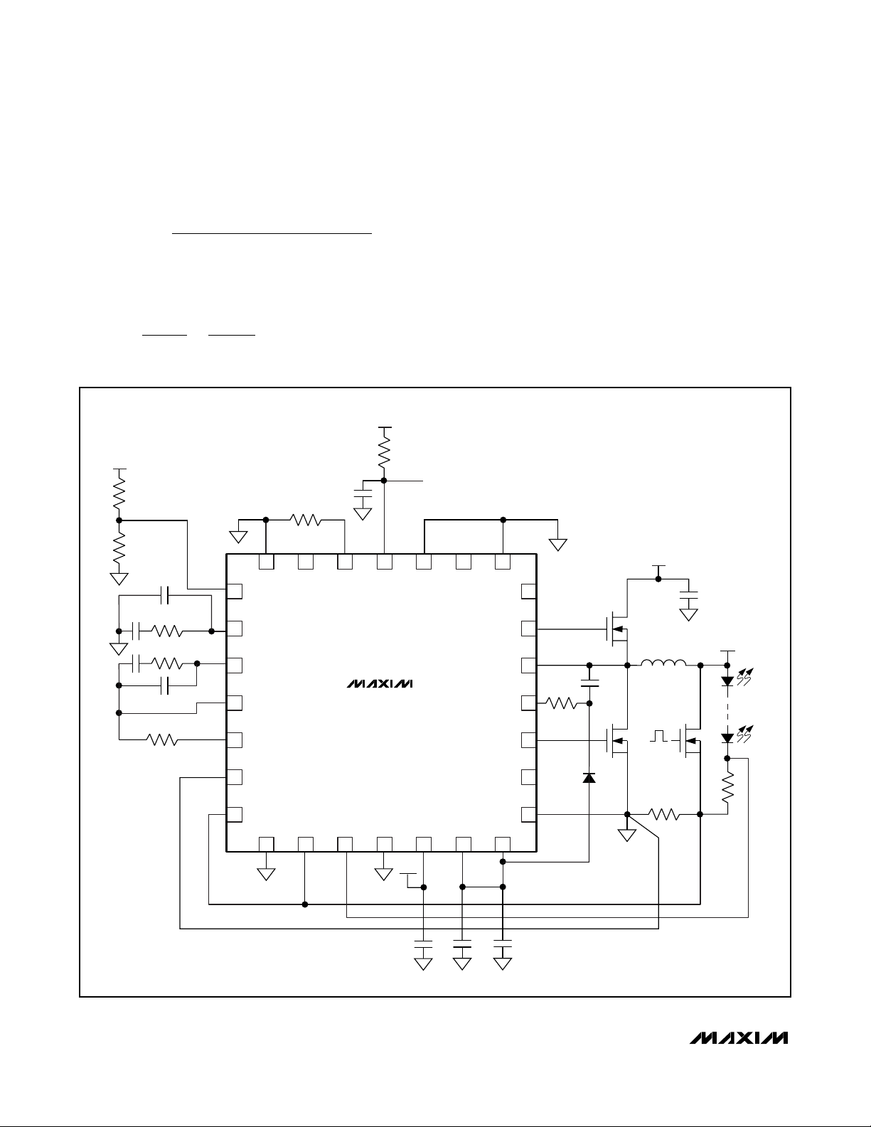
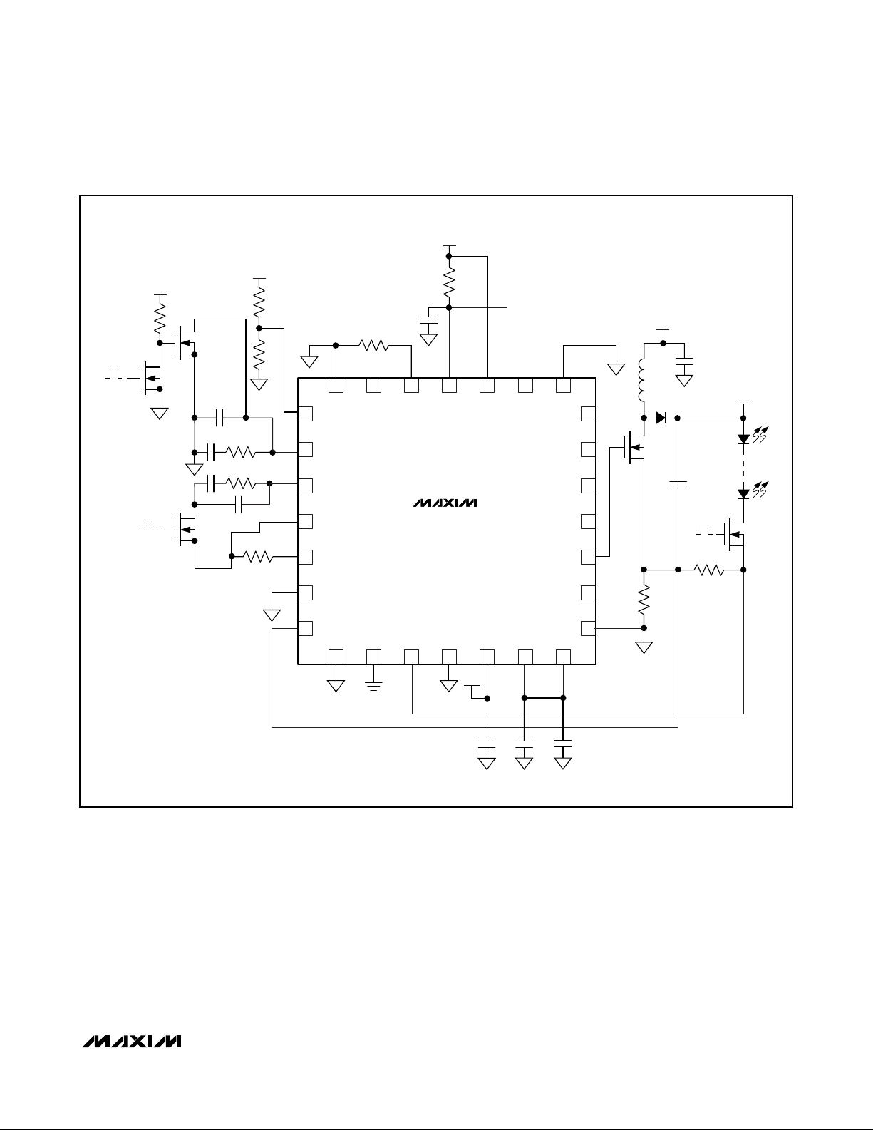
PWM Dimming
Even though the MAX16821A/MAX16821B/MAX16821C
do not have a separate PWM input, PWM dimming can
be easily achieved by means of simple external circuitry.
See Figures 10 and 11.
High-Power Synchronous HBLED
Drivers with Rapid Current Pulsing
20 ______________________________________________________________________________________
Figure 10. Low-Side Buck LED Driver with PWM Dimming (Patent Pending)
VfL
××
R
≤
CF
AR V V g
RAMP SW
( )
×× − ×
V
LED IN m
S
f
C
V
LED
R
R9
R10
C10
C9
V
RAMP
C11
R6
S
R9
R7
C8
. =×
V
LED
××
2
L
π
15
OVI
16
CLP
EAOUT
17
EAN
18
19
DIFF
×××
34 5
I.C. OUTV RT/SYNC EN MODE CLKOUT SGND
gR
mCF
C3
R3
12
1314
V
CC
R4
11
MAX16821A
MAX16821B
MAX16821C
ON/OFF
9
10
8
N.C.
BST
7
DH
6
5
LX
C4
R5
4
3
DL
20
CSN
CSP
21
SGND SENSE- SENSE+ SGND IN V
22 23
24 25 26
CC
27 28
V
IN
N.C.
PGND
V
DD
2
1
D2
7V TO 28V
Q1
PWM DIM
Q2
V
IN
C2
V
L1
R1
LED
LED
STRING
Q3
R2
C6 C5
C7
Power Dissipation
Calculate power dissipation in the MAX16821A/
MAX16821B/MAX16821C as a product of the input voltage and the total VCCregulator output current (ICC).
ICCincludes quiescent current (IQ) and gate-drive current (IDD):
PD= VINx I
CC
ICC= IQ+ [fSWx (QG1+ QG2)]
where Q
G1
and QG2are the total gate charge of the
low-side and high-side external MOSFETs at V
GATE
=
5V, IQis the supply current, and fSWis the switching
frequency of the LED driver.
Use the following equation to calculate the maximum
power dissipation (P
DMAX
) in the chip at a given ambi-
ent temperature (T
A
):
P
DMAX
= 34.5 x (150 – TA) mW
MAX16821A/MAX16821B/MAX16821C
High-Power Synchronous HBLED
Drivers with Rapid Current Pulsing
______________________________________________________________________________________ 21
PWM DIM
Figure 11. Boost LED Driver with PWM Dimming
V
R10
PWM DIM
V
CC
V
LED
CC
R8
Q5
R9
Q4
C11
C10
R7
R6
C9
C8
Q3
R5
15
OVI
16
CLP
EAOUT
17
EAN
18
19
DIFF
R3
1314
I.C. OUTV RT/SYNC EN MODE CLKOUT SGND
C3
12
MAX16821A
MAX16821B
MAX16821C
R4
ON/OFF
9
10
11
8
N.C.
BST
7
DH
6
5
LX
4
3
DL
L1
V
IN
7V TO 28V
D1
Q1
C2
C1
PWM DIM
R2
V
LED
Q2
LED
STRING
20
CSN
CSP
21
SGND SENSE- SENSE+ SGND IN V
22 23
24 25 26
2
N.C.
PGND
1
V
CC
DD
27 28
V
IN
C6 C5
C7
R1
MAX16821A/MAX16821B/MAX16821C
PCB Layout
Use the following guidelines to layout the LED driver.
1) Place the IN, V
CC
, and VDDbypass capacitors
close to the MAX16821A/MAX16821B/MAX16821C.
2) Minimize the area and length of the high-current
switching loops.
3) Place the necessary Schottky diodes that are connected across the switching MOSFETs very close to
the respective MOSFET.
4) Use separate ground planes on different layers of
the PCB for SGND and PGND. Connect both of
these planes together at a single point and make
this connection under the exposed pad of the
MAX16821A/MAX16821B/MAX16821C.
5) Run the current-sense lines CSP and CSN very
close to each other to minimize the loop area. Run
the sense lines SENSE+ and SENSE- close to each
other. Do not cross these critical signal lines with
power circuitry. Sense the current right at the pads
of the current-sense resistors. The current-sense
signal has a maximum amplitude of 27.5mV. To prevent contamination of this signal from high dv/dt
and high di/dt components and traces, use a
ground plane layer to separate the power traces
from this signal trace.
6) Place the bank of output capacitors close to the load.
7) Distribute the power components evenly across the
board for proper heat dissipation.
8) Provide enough copper area at and around the
switching MOSFETs, inductor, and sense resistors
to aid in thermal dissipation.
9) Use 2oz or thicker copper to keep trace inductances
and resistances to a minimum. Thicker copper conducts heat more effectively, thereby reducing thermal
impedance. Thin copper PCBs compromise efficiency
in applications involving high currents.
High-Power Synchronous HBLED
Drivers with Rapid Current Pulsing
22 ______________________________________________________________________________________
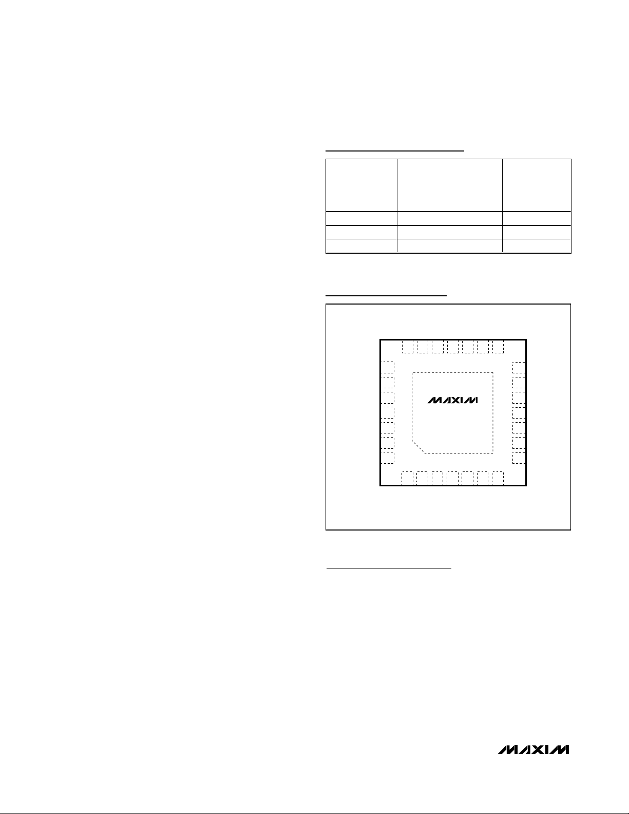
Selector Guide
Chip Information
PROCESS: BiCMOS
MAX16821A
MAX16821B
MAX16821C
TQFN
TOP VIEW
26
27
25
24
10
9
11
N.C.
BST
LX
DH
N.C.
12
PGND
CSN
EAN
EAOUT
CSP
CLP
OVI
12
SGND
4567
2021 19 17 16 15
IN
V
CC
RT/SYNC
EN
MODE
CLKOUT
DL
DIFF
3
18
28
8
V
DD
SGND
*EP = EXPOSED PAD.
*EP
+
SENSE+
23
13
OUTV
SENSE-
22
14
I.C.
SGND
Pin Configuration
PART
MAX16821A 0.60 1
MAX16821B 0.10 6
MAX16821C 0.03 20
DIFFERENTIAL
SET VALUE
(V
SENSE+
DIFFERENTIAL
- V
(V)
SENSE-
)
AMP GAIN
(V/V)
MAX16821A/MAX16821B/MAX16821C
High-Power Synchronous HBLED
Drivers with Rapid Current Pulsing
______________________________________________________________________________________ 23
Typical Operating Circuit
V
CC
V
LED
R9
R10
C10
C9
C11
15
OVI
R9
R7
C8
R6
16
CLP
EAOUT
17
EAN
18
19
DIFF
R3
1314
I.C. OUTV RT/SYNC EN MODE CLKOUT SGND
R4
C3
12
MAX16821A
MAX16821B
MAX16821C
ON/OFF
V
IN
10
11
9
8
N.C.
7
DH
6
5
LX
BST
DL
R5
4
3
7V TO 28V
C2
Q1
V
L1
C4
Q2
C1
LED
LED
STRING
20
CSN
CSP
21
SGND SENSE- SENSE+ SGND IN V
22 23
24 25 26
V
C7
IN
CC
27 28
C6 C5
N.C.
PGND
V
DD
2
1
D2
R1
R2
MAX16821A/MAX16821B/MAX16821C
High-Power Synchronous HBLED
Drivers with Rapid Current Pulsing
24 ______________________________________________________________________________________
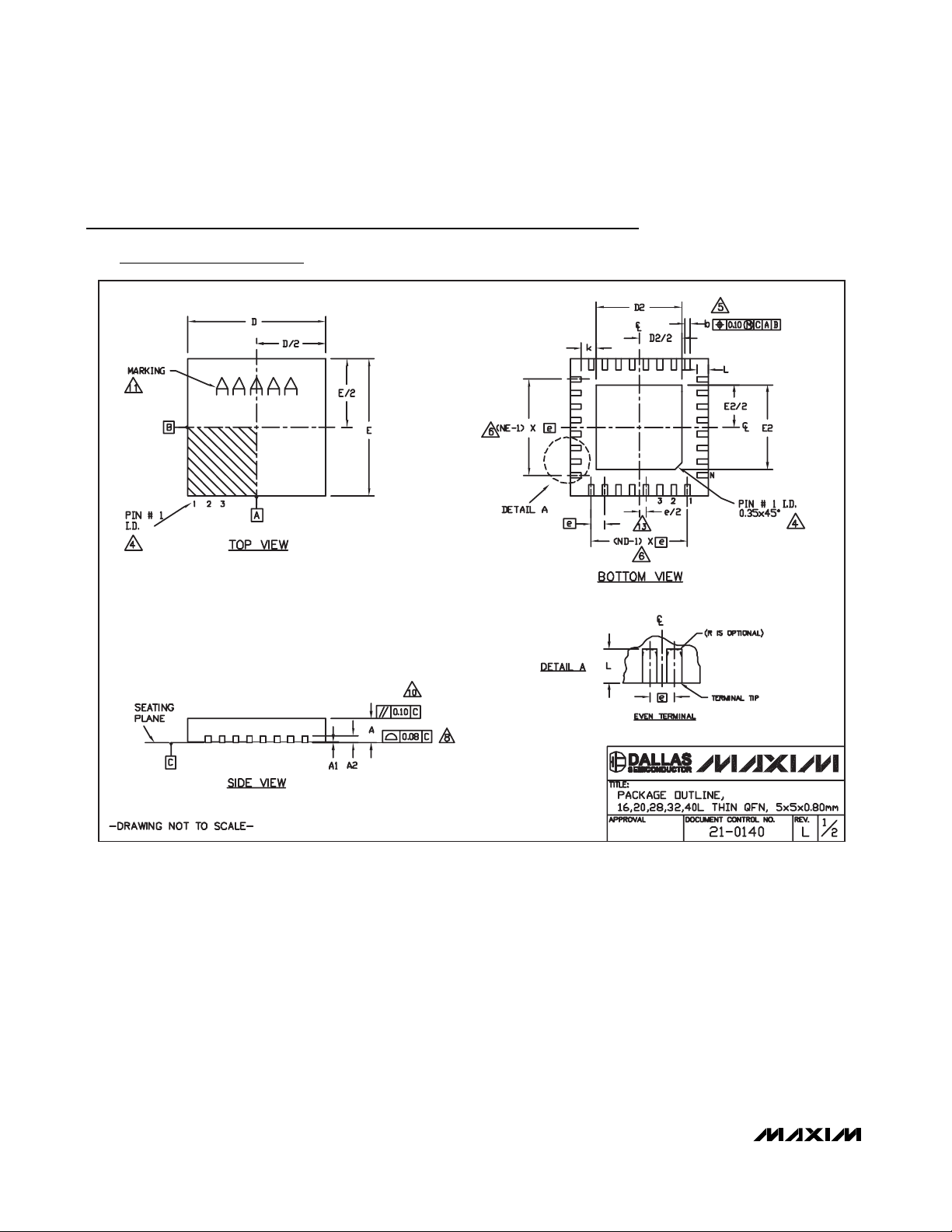
Package Information
(The package drawing(s) in this data sheet may not reflect the most current specifications. For the latest package outline information,
go to www.maxim-ic.com/packages
.)
QFN THIN.EPS
MAX16821A/MAX16821B/MAX16821C
High-Power Synchronous HBLED
Drivers with Rapid Current Pulsing
Maxim cannot assume responsibility for use of any circuitry other than circuitry entirely embodied in a Maxim product. No circuit patent licenses are
implied. Maxim reserves the right to change the circuitry and specifications without notice at any time.
Maxim Integrated Products, 120 San Gabriel Drive, Sunnyvale, CA 94086 408-737-7600 ____________________
25
© 2007 Maxim Integrated Products is a registered trademark of Maxim Integrated Products, Inc.
Heaney
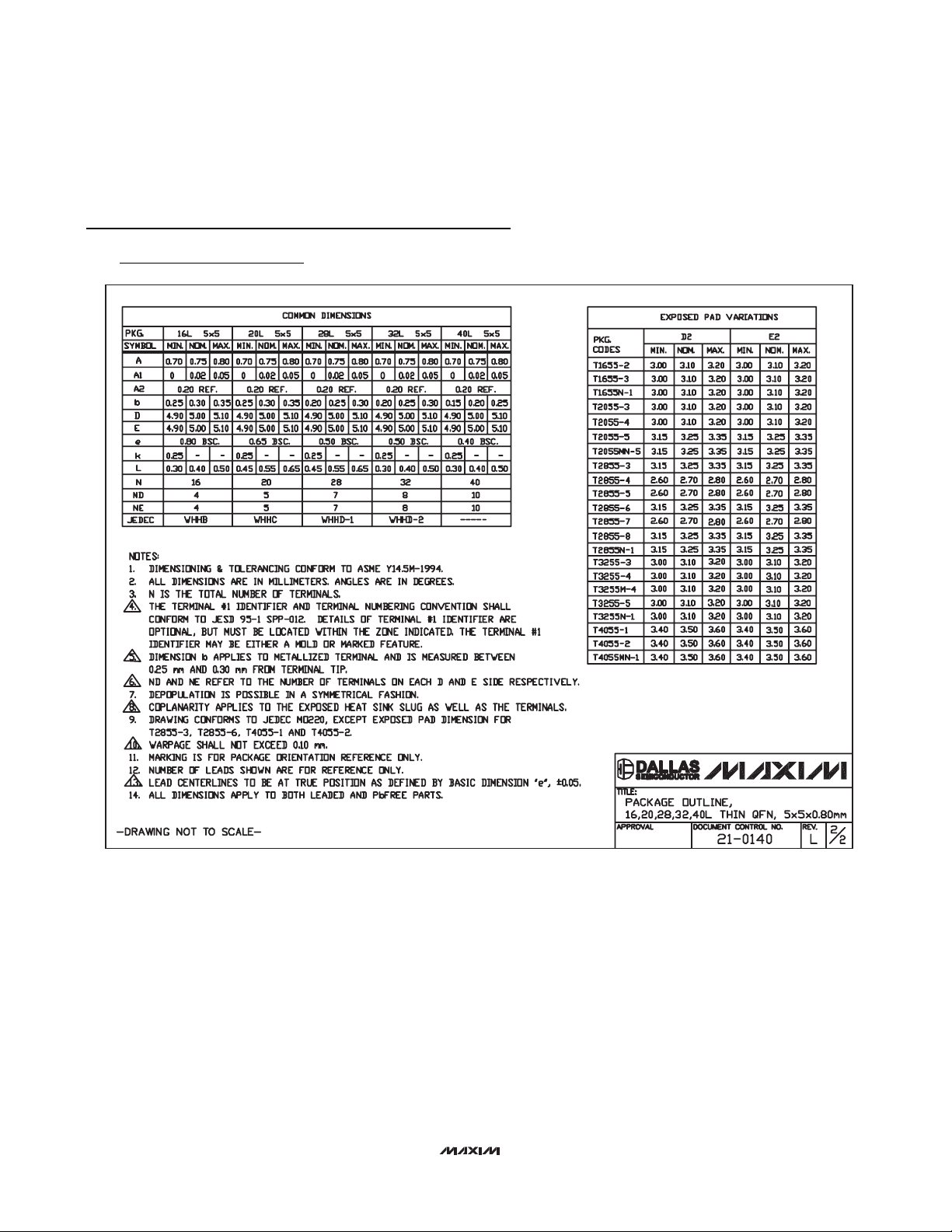
Package Information (continued)
(The package drawing(s) in this data sheet may not reflect the most current specifications. For the latest package outline information,
go to www.maxim-ic.com/packages
.)
 Loading...