

General Description
The MAX16819/MAX16820, step-down constant-current
high-brightness LED (HB LED) drivers provide a costeffective solution for automotive interior/exterior lighting,
architectural and ambient lighting, LED bulbs such as
MR16 and other LED illumination applications.
The MAX16819/MAX16820 operate from a 4.5V to 28V
input voltage range and feature a 5V/10mA on-board
regulator. A high-side current-sense resistor adjusts the
output current and a dedicated PWM input (DIM)
enables a wide range of pulsed dimming.
The MAX16819/MAX16820 are well suited for applications requiring a wide input voltage range. The high-side
current-sensing and an integrated current-setting circuitry minimize the number of external components while
delivering an LED current with ±5% accuracy. A hysteretic control algorithm ensures excellent input-supply
rejection and fast response during load transients and
PWM dimming. The MAX16819 features a 30% inductor
current ripple and the MAX16820 features a 10% current
ripple. These devices operate up to 2MHz switching frequency, thus allowing for small component size.
The MAX16819/MAX16820 operate over the -40°C to
+125°C automotive temperature range and are available in 3mm x 3mm x 0.8mm, 6-pin TDFN packages.
Applications
Architectural, Industrial, and Ambient Lighting
Automotive RCL, DRL, and Fog Lights
MR16 and Other LED Bulbs
Indicators and Emergency Lighting
Features
o High-Side Current Sense
o Dedicated Dimming Control Input
o 20kHz Maximum Dimming Efficiency
o Hysteretic Control: No Compensation
o Up to 2MHz Switching Frequency
o ±5% LED Current Accuracy
o Adjustable Constant LED Current
o 4.5V to 28V Input Voltage Range
o Over 25W Output Power
o 5V, 10mA On-Board Regulator
o -40°C to +125°C Operating Temperature Range
Note: All devices are specified over the -40°C to +125°C operating temperature range.
+
Denotes lead-free package.
*
EP = Exposed paddle.
MAX16819/MAX16820
2MHz High-Brightness LED Drivers with
High-Side Current Sense and 5000:1 Dimming
________________________________________________________________
Maxim Integrated Products
1
1
+
23
654
DIM
CSN
IN
GND
DRV
V
CC
MAX16819
MAX16820
TDFN
TOP VIEW
PART PIN-PACKAGE PKG CODE
TOP
MARK
MAX16819ATT+T 6 TDFN–EP* T633-2 +ATB
MAX16820ATT+T 6 TDFN-EP* T633-2 +ATC
Pin Configuration
Ordering Information
MAX16819
MAX16820
IN
CSN
DIM
V
CC
C
IN
DRV
GND
C
VCC
V
IN
LR
SENSE
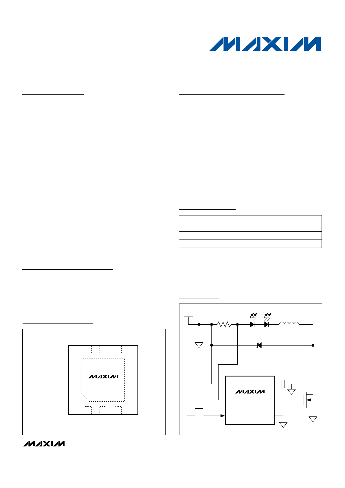
Typical Operating Circuit
19-0706; Rev 1; 3/07
For pricing, delivery, and ordering information, please contact Maxim/Dallas Direct! at
1-888-629-4642, or visit Maxim’s website at www.maxim-ic.com.
MAX16819/MAX16820
2MHz High-Brightness LED Drivers with
High-Side Current Sense and 5000:1 Dimming
2 _______________________________________________________________________________________
ABSOLUTE MAXIMUM RATINGS
ELECTRICAL CHARACTERISTICS
(VIN= 12V, V
DIM
= VIN, C
VCC
= 1µF, R
SENSE
= 0.5Ω, TA= TJ= -40°C to +125°C, unless otherwise noted. Typical values are at
T
A
= +25°C.) (Note 1)
Stresses beyond those listed under “Absolute Maximum Ratings” may cause permanent damage to the device. These are stress ratings only, and functional
operation of the device at these or any other conditions beyond those indicated in the operational sections of the specifications is not implied. Exposure to
absolute maximum rating conditions for extended periods may affect device reliability.
IN, CSN, DIM to GND .............................................-0.3V to +30V
V
CC
, DRV to GND ....................................................-0.3V to +6V
CSN to IN...............................................................-0.3V to +0.3V
Maximum Current into Any Pin
(except IN, V
CC
, and DRV)............................................±20mA
Continuous Power Dissipation (T
A
= +70°C)
6-Pin TDFN (derate 18.17mW/
oC*
above +70°C).......1454mW
Operating Temperature Range .........................-40°C to +125°C
Junction Temperature......................................................+150°C
Storage Temperature Range .............................-65°C to +150°C
Lead Temperature (soldering, 10s) .................................+300°C
Pin-to-Pin ESD Ratings (HB Model).....................................2.5kV
*As per JEDEC51 Standard (Single-Layer Board).
PARAMETER SYMBOL CONDITIONS MIN TYP MAX UNITS
Input Voltage Range V
IN
4.5 28.0 V
Maximum Current Regulator
Switching Frequency
f
SW
2 MHz
Ground Current I
GND
DRV open 1.5 mA
Supply Current I
IN
V
DIM
< 0.6V 425 µA
VIN = V
CSN
= V
DIM
, VIN rising from 4V until
V
DRV
> VCC - 0.5V
4.7 5.0
Undervoltage Lockout UVLO
V
IN
= V
CSN
= V
DIM
, VIN falling from 6V,
V
DRV
< 0.5V
4.5
V
Undervoltage Lockout Hysteresis 0.5 V
SENSE COMPARATOR
(VIN - V
CSN
) rising from 0V until V
DRV
<
0.5V (MAX16820)
195 210 225
Sense Voltage Threshold High V
SNSHI
(VIN - V
CSN
) rising from 0V until V
DRV
<
0.5V (MAX16819)
213 230 246
mV
(VIN - V
CSN
) falling from 0.26V until V
DRV
>
(V
CC
- 0.5V) (MAX16820)
176 190 204
Sense Voltage Threshold Low V
SNSLO
(VIN - V
CSN
) falling from 0.26V until V
DRV
>
(V
CC
- 0.5V) (MAX16819)
158 170 182
mV
Propagation Delay to Output
High
t
DPDH
Falling edge of (VIN - V
CSN
) from 0.26V to
0V to DRV high, C
DRV
= 1nF
82 ns
Propagation Delay to Output Low t
DPDL
Rising edge of (VIN - V
CSN
) from 0V to
0.26V to DRV low, C
DRV
= 1nF
82 ns
Current-Sense Input Current I
CSN
(VIN - V
CSN
) = 200mV 1 µA
MAX16819 56 70 mV
Current-Sense Threshold
Hysteresis
CS
HYS
MAX16820 17 35 mV
MAX16819/MAX16820
2MHz High-Brightness LED Drivers with
High-Side Current Sense and 5000:1 Dimming
_______________________________________________________________________________________ 3
PARAMETER SYMBOL CONDITIONS MIN TYP MAX UNITS
GATE DRIVER
Gate Driver Source Current V
CSN
= VIN, V
DRV
= 0.5 x V
CC
0.5 A
Gate Driver Sink Current V
CSN
= VIN - 250mV, V
DRV
= 0.5 x V
CC
1A
Gate Driver Output-Voltage High V
OH
I
DRV
= 10mA VCC - 0.5 V
Gate Driver Output-Voltage Low V
OL
I
DRV
= -10mA 0.5 V
DIM INPUT
Maximum DIM Frequency f
DIM
20 kHz
DIM Input-Voltage High V
IH
V
CSN
= VIN, increase DIM until V
DRV
>
(V
CC
- 0.5V)
2.8 V
DIM Input-Voltage Low V
IL
V
CSN
= VIN, decrease DIM until
V
DRV
< 0.5V
0.6 V
DIM Hysteresis DIM
HYS
200 mV
DIM Turn-On Time t
DIMON
DIM rising edge to V
DRV
= 0.5 x VCC,
C
DRV
= 1nF
100 ns
DIM Turn-Off Time t
DIMOFF
DIM falling edge to V
DRV
= 0.5 x VCC,
C
DRV
= 1nF
100 ns
DIM Input Leakage High V
DIM
= V
IN
10 µA
DIM Input Leakage Low V
DIM
= 0V -1 +1 µA
VCC REGULATOR
I
VCC
= 0.1mA to 10mA, VIN = 5.5V to 28V 4.5 5.5 V
Regulator Output Voltage V
CC
I
VCC
= 0.1mA to 10mA, VIN = 4.5V to 28V 4.0 5.5 V
Load Regulation I
VCC
= 0.1mA to 10mA, VIN = 12V 4 Ω
Line Regulation VIN = 6V to 28V, I
VCC
= 10mA 11 mV
Power-Supply Rejection Ratio PSRR VIN = 12V, I
VCC
= 5mA, fIN = 10kHz -35 dB
VIN = 4.5V, VCC = 0V 45 mA
Current Limit I
LIM
VIN = 4.5V, VCC = 4V 18 mA
Regulator Startup Time t
STRAT
VCC = 0 to 4.5V 350 µs
ELECTRICAL CHARACTERISTICS (continued)
(VIN= 12V, V
DIM
= VIN, C
VCC
= 1µF, R
SENSE
= 0.5Ω, TA= TJ= -40°C to +125°C, unless otherwise noted. Typical values are at
T
A
= +25°C.) (Note 1)
Note 1: All devices are 100% production tested at T
J
= +25°C and +125°C. Limits to -40°C are guaranteed by design.

MAX16819/MAX16820
2MHz High-Brightness LED Drivers with
High-Side Current Sense and 5000:1 Dimming
4 _______________________________________________________________________________________
Typical Operating Characteristics
(VIN= V
DIM
= 12V, C
VCC
= 1µF, R
SENSE
= 0.5Ω connected between IN and CSN. Typical values at TA= +25°C, unless otherwise
noted.)
EFFICIENCY vs. V
IN
MAX16819 toc01
VIN (V)
EFFICIENCY (%)
252010 15
65
70
75
80
90
85
95
100
60
530
LED 5
LED 4
L = 47µH
DRV SWITCHING FREQUENCY
vs. V
IN
MAX16819 toc02
VIN (V)
DRV SWITCHING FREQUENCY (kHz)
242016128
100
200
300
400
600
500
700
800
900
1000
1100
1200
1300
1400
1500
0
428
L = 47µH
LED 5
LED 4
LED 3
LED 1
LED 2
LED CURRENT VARIATION vs. V
IN
MAX16819 toc03
VIN (V)
LED CURRENT VARIATION FROM SET CURRENT (%)
252010 15
-1.5
-1.0
-0.5
0
1.0
0.5
1.5
2.0
-2.0
530
LED 5
LED 4
LED 3
LED 2
LED 1
I
LED(NOMINAL)
= 400mA
L = 47µH
VCC vs. V
IN
MAX16819 toc04
VIN (V)
V
CC
(V)
25.022.517.5 20.0
10.0
12.5 15.07.5
4.6
4.7
4.8
4.9
5.0
5.1
5.2
5.3
5.4
5.5
4.5
5.0 27.5
I
LED
= 0
VCC vs. TEMPERATURE
MAX16819 toc05
TEMPERATURE (°C)
V
CC
(V)
1109565 80-10 5 20 35 50-25
5.31
5.32
5.33
5.34
5.35
5.36
5.37
5.38
5.39
5.40
5.30
-40 125
VIN = 24V
VIN = 12V
V
DIM
= 0V
SUPPLY CURRENT vs. V
IN
MAX16819 toc06
VIN (V)
SUPPLY CURRENT (µA)
24.5
12.5
20.516.58.5
50
100
150
200
250
300
0
4.5 28.5
V
DIM
= 0V
PWM DIMMING AT 200Hz
(10% DUTY CYCLE)
MAX16819 toc07
1ms/div
V
DIM
2V/div
0V
0A
I
LED
200mA/div
V
IN
= 12V, L = 47µH,
1 LED MAX16819
PWM DIMMING AT 200Hz
(90% DUTY CYCLE)
MAX16819 toc08
1ms/div
V
DIM
2V/div
0V
0A
I
LED
200mA/div
V
IN
= 12V, L = 47µH,
1 LED MAX16819

MAX16819/MAX16820
PWM DIMMING AT 20kHz
(10% DUTY CYCLE)
MAX16819 toc12
10µs/div
V
DIM
2V/div
0V
0A
I
LED
200mA/div
V
IN
= 24V, L = 47µH,
4 LEDS MAX16820
PWM DIMMING AT 20kHz
(90% DUTY CYCLE)
MAX16819 toc13
10µs/div
V
DIM
2V/div
0V
0A
I
LED
200mA/div
V
IN
= 24V, L = 33µH,
4 LEDS MAX16820
2MHz High-Brightness LED Drivers with
High-Side Current Sense and 5000:1 Dimming
_______________________________________________________________________________________
5
PWM DIMMING AT 200Hz
(1% DUTY CYCLE)
MAX16819 toc09
10µs/div
V
DIM
2V/div
0V
0A
I
LED
200mA/div
V
IN
= 12V, L = 47µH,
1 LED MAX16819
PWM DIMMING EXPANDED
(50% DUTY CYCLE)
MAX16819 toc10
1µs/div
V
DIM
2V/div
0V
0A
I
LED
200mA/div
V
IN
= 24V, L = 33µH,
4 LEDS MAX16820
PWM DIMMING EXPANDED
(50% DUTY CYCLE)
MAX16819 toc11
4µs/div
V
DIM
2V/div
0V
0A
I
LED
200mA/div
V
IN
= 12V, L = 47µH,
1 LED MAX16819
I
LED
VARIATION vs. TEMPERATURE
MAX16819 toc14
TEMPERATURE (°C)
LED CURRENT VARIATION FROM SET CURRENT (%)
11095-25 -10 5 35 50 6520 80
-1.5
-1.0
-0.5
0
0.5
1.0
1.5
2.0
-2.0
-40 125
V
IN
= 24V
V
IN
= 12V
V
DIM
= 0V
I
LED(NOMINAL)
= 400mA
L = 47µH
Typical Operating Characteristics (continued)
(VIN= V
DIM
= 12V, C
VCC
= 1µF, R
SENSE
= 0.5Ω connected between IN and CSN. Typical values at TA= +25°C, unless otherwise
noted.)

MAX16819/MAX16820
2MHz High-Brightness LED Drivers with
High-Side Current Sense and 5000:1 Dimming
6 _______________________________________________________________________________________
MAX16819
MAX16820
REGULATOR
CS
COMPARATOR
UVLO
COMPARATOR
1.23V
BANDGAP
REF
GATE
DRIVER
DIM
BUFFER
V
CC
DRV
GND
+
-
-
+
CSN
IN
DIM
Pin Description
Functional Diagram
PIN NAME FUNCTION
1 IN Positive Supply Voltage Input. Bypass with a 1µF or higher value capacitor to GND.
2 CSN Current-Sense Input
3 DIM
Logic-Level Dimming Input. Drive DIM low to turn off the current regulator. Drive DIM high to enable
the current regulator.
4 GND Ground
5 DRV Gate Drive Output. Connect to the gate of an external n-channel MOSFET.
6VCCVoltage Regulator Output. Connect a 1µF capacitor from VCC to GND.
EP —
Exposed Paddle. Connect to a large-area ground plane for improved power dissipation. Do not use
as the only ground connection for the device.
Detailed Description
The MAX16819/MAX16820 are step-down, constantcurrent, high-brightness LED (HB LED) drivers. These
devices operate from a 4.5V to 28V input voltage range
and provide up to 0.5A of source and 1A of sink drive
capability to the gate of an external MOSFET. A highside current-sense resistor sets the output current and
a dedicated PWM dimming input (DIM) allows for a
wide range of independent pulsed dimming.
The high-side current-sensing scheme and on-board
current-setting circuitry minimize the number of external components while delivering LED current with a
±5% accuracy, using a 1% sense resistor. See the
Functional Diagram
.

Undervoltage Lockout (UVLO)
The MAX16819/MAX16820 include a 4.5V undervoltage
lockout (UVLO) with 500mV hysteresis. When VINfalls
below 4.5V, DRV goes low, turning off the external n-channel MOSFET. DRV goes high once V
IN
is 5V or higher.
5V Regulator
VCCis the output of a 5V regulator capable of sourcing
10mA. Bypass VCCto GND with a 1µF capacitor.
DIM Input
The MAX16819/MAX16820 allow dimming with a PWM
signal at the DIM input. A logic level below 0.6V at DIM
forces the MAX16819/MAX16820’s DRV output low,
turning off the LED current. To turn the LED current on,
the logic level at DIM must be at least 2.8V.
Applications Information
Selecting R
SENSE
to Set the LED Current
The MAX16819/MAX16820 feature a programmable LED
current using a resistor connected between IN and CSN.
Use the following equation to calculate the sense resistor:
For the values of V
SNSHI
and V
SNSLO,
see the
Electrical
Characteristics
.
Current Regulator Operation
The MAX16819/MAX16820 regulate the LED output
current using an input comparator with hysteresis
(Figure 1). As the current through the inductor ramps
up and the voltage across the sense resistor reaches
the upper threshold, the voltage at DRV goes low, turning off the external MOSFET. The MOSFET turns on
again when the inductor current ramps down through
the freewheeling diode until the voltage across the
sense resistor equals the lower threshold. Use the following equation to determine the operating frequency:
where n = number of LEDs, V
LED
= forward voltage
drop of one LED, and ∆V = (V
SNSHI
- V
SNSLO
).
For proper component selection, please use the design
tool available at: http://www.maxim-ic.com/MAX1681920-Tool.
f
VnV nV R
VVL
SW
IN LED LED SENSE
IN
=
−×
()
×× ×
××∆
R
VVV
IA
SENSE
SNSHI SNSLO
LED
Ω
()
=
+
()()
()
1
2
MAX16819/MAX16820
2MHz High-Brightness LED Drivers with
High-Side Current Sense and 5000:1 Dimming
_______________________________________________________________________________________ 7
HYSTERETIC MODE
AVG. LED
CURRENT
1
f
SW
T
SW
=
I
LED
t
t
V
DIM
∆I
Figure 1. Current Regulator Operation

MAX16819/MAX16820
MOSFET Selection
The MAX16819/MAX16820’s gate driver is capable of
sourcing 0.5A and sinking 1A of current. MOSFET selection is based on the maximum input operating voltage
V
IN
, output current I
LED
, and operating switching frequency. Choose a MOSFET that has a higher breakdown voltage than the maximum operation voltage, low
R
DS(ON)
, and low total charge for better efficiency.
MOSFET threshold voltage must be adequate if operated at the low end of the input-voltage operating range.
Freewheeling Diode Selection
The forward voltage of the freewheeling diode should
be as low as possible for better efficiency. A Schottky
diode is a good choice as long as the breakdown voltage is high enough to withstand the maximum operating voltage.
The forward current rating of the diode must be at least
equal to the maximum LED current.
LED Current Ripple
The LED current ripple is equal to the inductor current
ripple. In cases when a lower LED current ripple is
needed, a capacitor can be placed across the LED terminals.
PCB Layout Guidelines
Careful PCB layout is critical to achieve low switching
losses and stable operation. Use a multilayer board
whenever possible for better noise immunity. Minimize
ground noise by connecting high-current ground
returns, the input bypass-capacitor ground lead, and
the output-filter ground lead to a single point (star
ground configuration). In normal operation, there are
two power loops. One is formed when the MOSFET is
on and the high current flows through IN—R
SENSE
—
LEDs—Inductor—MOSFET—GND. The other loop is
formed when the MOSFET is off when the high current
circulates through R
SENSE
—LEDs—Inductor—freewheeling diode. To minimize noise interaction, each
loop area should be as small as possible.
Place R
SENSE
as close as possible to the input filter
and IN. For better noise immunity, a Kelvin connection
is strongly recommended between CSN and R
SENSE
.
Connect the exposed paddle to a large-area ground
plane for improved power dissipation.
2MHz High-Brightness LED Drivers with
High-Side Current Sense and 5000:1 Dimming
8 _______________________________________________________________________________________
Chip Information
PROCESS: BiCMOS

MAX16819/MAX16820
2MHz High-Brightness LED Drivers with
High-Side Current Sense and 5000:1 Dimming
_______________________________________________________________________________________ 9
Package Information
(The package drawing(s) in this data sheet may not reflect the most current specifications. For the latest package outline information
go to www.maxim-ic.com/packages
.)
6, 8, &10L, DFN THIN.EPS
H
1
2
21-0137
PACKAGE OUTLINE, 6,8,10 & 14L,
TDFN, EXPOSED PAD, 3x3x0.80 mm

MAX16819/MAX16820
2MHz High-Brightness LED Drivers with
High-Side Current Sense and 5000:1 Dimming
Maxim cannot assume responsibility for use of any circuitry other than circuitry entirely embodied in a Maxim product. No circuit patent licenses are
implied. Maxim reserves the right to change the circuitry and specifications without notice at any time.
10
____________________Maxim Integrated Products, 120 San Gabriel Drive, Sunnyvale, CA 94086 408-737-7600
© 2007 Maxim Integrated Products is a registered trademark of Maxim Integrated Products, Inc.
Package Information (continued)
(The package drawing(s) in this data sheet may not reflect the most current specifications. For the latest package outline information
go to www.maxim-ic.com/packages
.)
COMMON DIMENSIONS
SYMBOL
MIN. MAX.
A 0.70 0.80
D 2.90 3.10
E 2.90 3.10
A1
0.00 0.05
L 0.20 0.40
PKG. CODE N D2 E2 e JEDEC SPEC b [(N/2)-1] x e
PACKAGE VARIATIONS
0.25 MIN.k
A2 0.20 REF.
2.30±0.101.50±0.106T633-1 0.95 BSC MO229 / WEEA 1.90 REF0.40±0.05
1.95 REF0.30±0.050.65 BSC2.30±0.108T833-1
2.00 REF0.25±0.050.50 BSC2.30±0.1010T1033-1
2.40 REF0.20±0.05- - - - 0.40 BSC1.70±0.10 2.30±0.1014T1433-1
1.50±0.10
1.50±0.10
MO229 / WEEC
MO229 / WEED-3
0.40 BSC - - - - 0.20±0.05 2.40 REFT1433-2 14 2.30±0.101.70±0.10
T633-2 6 1.50±0.10 2.30±0.10
0.95 BSC MO229 / WEEA
0.40±0.05 1.90 REF
T833-2 8 1.50±0.10 2.30±0.10 0.65 BSC MO229 / WEEC 0.30±0.05 1.95 REF
T833-3 8 1.50±0.10 2.30±0.10 0.65 BSC MO229 / WEEC 0.30±0.05 1.95 REF
-DRAWING NOT TO SCALE-
H
2
2
21-0137
PACKAGE OUTLINE, 6,8,10 & 14L,
TDFN, EXPOSED PAD, 3x3x0.80 mm
2.30±0.10
MO229 / WEED-3
2.00 REF0.25±0.05
0.50 BSC
1.50±0.1010T1033-2
Revision History
Pages changed at Rev 1: 1, 4, 10
 Loading...