

_______________General Description
The MAX1680/MAX1681 inductorless switched-capacitor voltage converters either invert an input voltage of
+2.0V to +5.5V or double it while supplying up to
125mA output current. They have a selectable-frequency option that allows the use of small capacitors: 4.7µF
(MAX1680), 1µF (MAX1681). With their high output current capability, these charge-pump devices are suitable replacements for inductor-based regulators, which
require more expensive external components and additional board space.
The devices’ equivalent output resistance (typically
3.5Ω) allows them to deliver as much as 125mA with
only a 440mV drop. A shutdown feature reduces quiescent current to less than 1µA. The MAX1680/MAX1681
are available in 8-pin SO packages. For devices that
deliver up to 50mA in smaller µMAX packages, refer to
the MAX860/MAX861 data sheet.
________________________Applications
Local Negative Supplies
Interface Power Supplies
Op-Amp Power Supplies
MOSFET Bias
____________________________Features
♦ Selectable Switching Frequencies:
125kHz/250kHz (MAX1680)
500kHz/1MHz (MAX1681)
♦ Allow Use of Small Capacitors
(1µF for the MAX1681)
♦ 125mA Output Current
♦ 3.5Ω Output Impedance
♦ 1µA Logic-Controlled Shutdown
♦ Configurable as Voltage Inverters or Doublers
♦ +2.0V to +5.5V Input Voltage Range
♦ Available in 8-Pin SO Packages
♦ 90% Efficiency
MAX1680/MAX1681
125mA, Frequency-Selectable,
Switched-Capacitor Voltage Converters
________________________________________________________________
Maxim Integrated Products
1
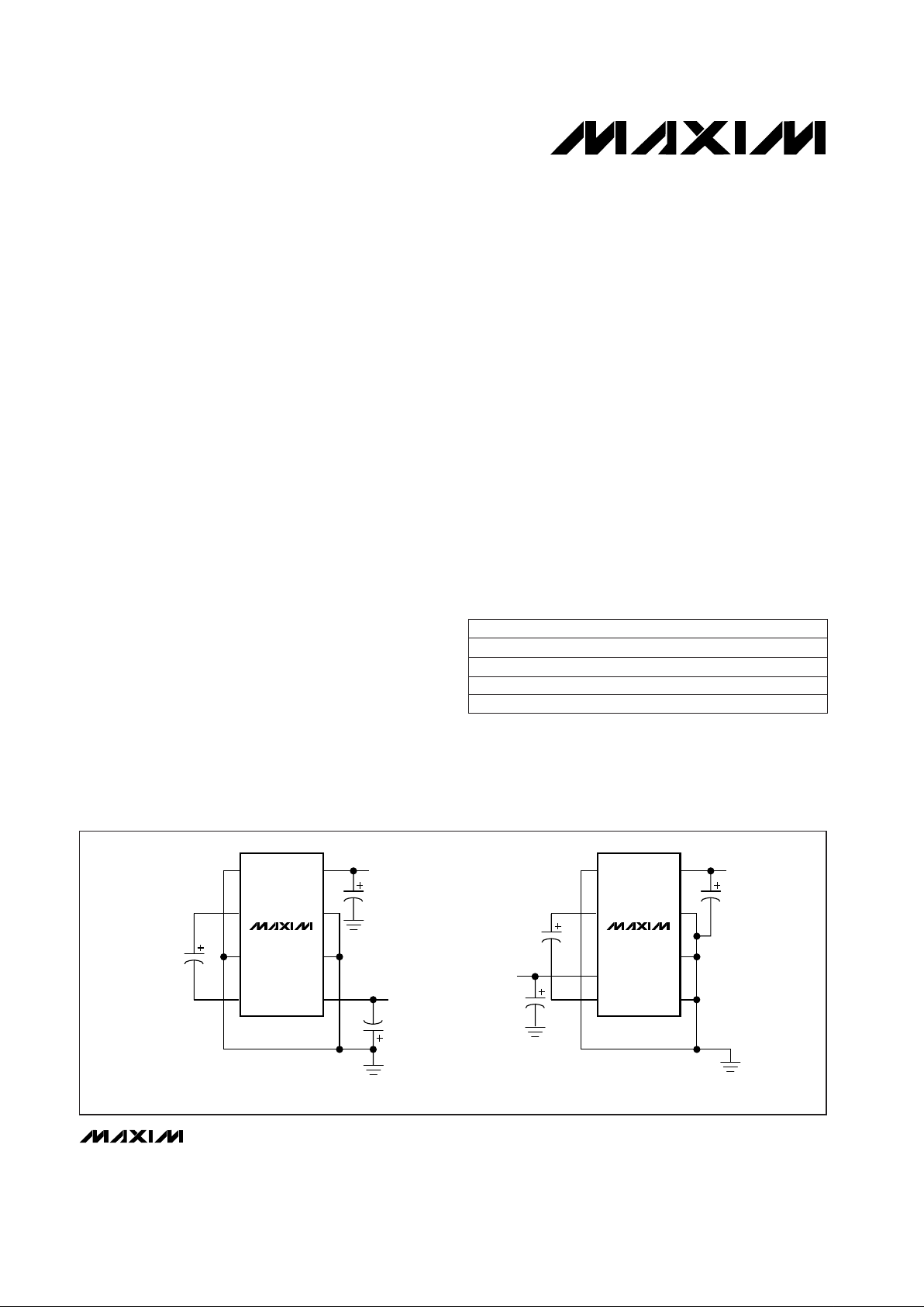
MAX1681
FSEL IN
CAP+ SHDN
GND
C1
1µF
+V
INPUT
+3V TO +5.5V
INVERTED
OUTPUT
VOLTAGE
C2
1µF
1µF
LV
CAP-
INVERTER CONFIGURATION
OUT
MAX1681
FSEL IN
CAP+ SHDN
GND
C1
1µF
C2
1µF
DOUBLED
OUTPUT
VOLTAGE
+V
INPUT
+4V TO +5.5V
NOTE: USE 4.7µF CAPACITORS FOR MAX1680
INPUT VOLTAGE RANGE: +2.5V TO +5.5V.
NOTE: USE 4.7µF CAPACITORS FOR MAX1680
INPUT VOLTAGE RANGE: +2.0V TO +5.5V.
1µF
LV
CAP-
DOUBLER CONFIGURATION
OUT
__________________________________________________Typical Operating Circuits
19-1247; Rev 0; 7/97
PART
MAX1680C/D
MAX1680ESA
MAX1681C/D
0°C to +70°C
-40°C to +85°C
0°C to +70°C
TEMP. RANGE PIN-PACKAGE
Dice*
8 SO
Dice*
______________Ordering Information
*
Contact factory for dice specifications.
Pin Configuration appears at end of data sheet.
MAX1681ESA -40°C to +85°C 8 SO
For free samples & the latest literature: http://www.maxim-ic.com, or phone 1-800-998-8800.
For small orders, phone 408-737-7600 ext. 3468.
V
MAX1680/MAX1681
125mA, Frequency-Selectable,
Switched-Capacitor Voltage Converters
2 _______________________________________________________________________________________
ABSOLUTE MAXIMUM RATINGS
ELECTRICAL CHARACTERISTICS
(
Typical Operating Circuits
(inverter configuration), FSEL = LV = GND, VIN= 5V, C1 = C2 = 10µF (MAX1680), C1 = C2 = 2.2µF
(MAX1681), T
A
= 0°C to +85°C, unless otherwise noted. Typical values are at TA= +25°C.)
Stresses beyond those listed under “Absolute Maximum Ratings” may cause permanent damage to the device. These are stress ratings only, and functional
operation of the device at these or any other conditions beyond those indicated in the operational sections of the specifications is not implied. Exposure to
absolute maximum rating conditions for extended periods may affect device reliability.
IN..............................................................................-0.3V to +6V
LV....................................................(V
OUT
- 0.3V) to (VIN+ 0.3V)
CAP+ ...........................................................-0.3V to (V
IN
+ 0.3V)
SHDN, FSEL ......................................(V
LV
- 0.3V) to (VIN+ 0.3V)
OUT, CAP-..................................................................-6V to 0.3V
Continuous Output Current ..............................................135mA
Output Short-Circuit Duration to GND (Note 1) ...................1sec
Continuous Power Dissipation (T
A
= +70°C)
SO (derate 5.88mW/°C above +70°C)..........................471mW
Operating Temperature Range ...........................-40°C to +85°C
Junction Temperature......................................................+150°C
Storage Temperature Range.............................-65°C to +160°C
Lead Temperature (soldering, 10sec).............................+300°C
I
LOAD
= 125mA
Inverter configuration,
RL= 1kΩ, LV = GND
LV = GND (Note 3)
FSEL = IN or LV
SHDN = IN
OUT = GND, SHDN = IN
CONDITIONS
375 500 625
750 1000 1250
94 125 156
187 250 313
4V
IH
V-3.75 -4.56V
LOAD
Output Voltage Under Load
(Note 2)
V
3.0 5.5
2.0 5.5
V
1V
IL
Shutdown, FSEL Thresholds
µA-1 1I
FSEL
Input Bias Current (FSEL)
Ω3.5 10R
OUT
Output Resistance (Note 2)
Ω1 5R
OUT(SHUT)
Output Resistance to Ground
in Shutdown
µA1I+
SHDN
Shutdown Current
µA-1 1I
SHDN
Input Bias Current (SHDN)
UNITSMIN TYP MAXSYMBOLPARAMETER
Doubler configuration,
RL= 1kΩ, LV = OUT
4.0 5.5
V
IN
2.5 5.5
Input Voltage Range
MAX1680
5.4
mA
10.8
FSEL = IN
(125kHz)
FSEL = LV
(250kHz)
MAX1681
21.6
43.2
I+
FSEL = IN
(500kHz)
Supply Current
FSEL = LV
(1MHz)
Note 1: Shorting OUT to IN may damage the device and should be avoided.
TA= +25°C
TA= +25°C
TA= +25°C
TA= +25°C
MAX1681
MAX1680
MAX1681
MAX1680
TA= +25°C
TA= +25°C
TA= +25°C
TA= +25°C
2.5 4.5
5 9
10 18
20 36
FSEL = LV
157 348
FSEL = IN
MAX1680
79 174
FSEL = LV
570 1490
kHz
FSEL = IN
MAX1681
f
OSC
Switching Frequency
285 745
mA
ELECTRICAL CHARACTERISTICS
(
Typical Operating Circuits
(inverter configuration), FSEL = LV = GND, VIN= 5V, C1 = C2 = 10µF (MAX1680), C1 = C2 = 2.2µF
(MAX1681), T
A
= -40°C to +85°C, unless otherwise noted.) (Note 4)
MAX1680/MAX1681
125mA, Frequency-Selectable,
Switched-Capacitor Voltage Converters
_______________________________________________________________________________________ 3
FSEL = IN
FSEL = LV
MAX1681
I
LOAD
= 125mA
21.6
mA
Inverter configuration,
RL= 1kΩ, LV = GND
43.2
Doubler configuration,
R
L
= 1kΩ, LV = OUT
MAX1681
FSEL = LV
FSEL = IN
MAX1680
LV = GND (Note 3)
FSEL = IN or LV
SHDN = IN
OUT = GND, SHDN = IN
CONDITIONS
I+
FSEL = IN
(500kHz)
Supply Current
FSEL = LV
(1MHz)
kHz
285 745
f
OSC
570 1490
79 174
157 348
Switching Frequency
4V
IH
V-3.75V
LOAD
Output Voltage Under Load
(Note 2)
3.0 5.5
V
2.0 5.5
4.0 5.5
V
IN
V
-1 1V
IL
Shutdown, FSEL Thresholds
µA-1 1I
FSEL
Input Bias Current (FSEL)
Ω10R
OUT
Output Resistance (Note 2)
Ω5R
OUT(SHUT)
Output Resistance in
Shutdown
µA1I+
SHDN
Shutdown Current
µA1I
SHDN
Input Bias Current (SHDN)
UNITSMIN TYP MAXSYMBOLPARAMETER
MAX1681
MAX1680
2.5 5.5
Input Voltage Range
MAX1681
MAX1680
MAX1680
5.4
10.8
FSEL = IN
(125kHz)
FSEL = LV
(250kHz)
ELECTRICAL CHARACTERISTICS (continued)
(
Typical Operating Circuits
(inverter configuration), FSEL = LV = GND, VIN= 5V, C1 = C2 = 10µF (MAX1680), C1 = C2 = 2.2µF
(MAX1681), T
A
= 0°C to +85°C, unless otherwise noted. Typical values are at TA= +25°C.)
Note 2: C1 and C2 are low-ESR (<0.2Ω) capacitors. Capacitor ESR adds to the circuit’s output resistance. Using capacitors with
higher ESR reduces output voltage and efficiency. The specified output resistance includes the C1 and C2 0.2Ω ESR.
Note 3: The typical threshold for V
INPUT
other than +5V is 0.35V
INPUT(VIL
= VIH).
Note 4: Specifications to -40°C are guaranteed by design, not production tested.
RL= 100Ω to GND, FSEL = IN
MAX1680
MAX1681
%
80
90
Power Efficiency
UNITSMIN TYP MAXSYMBOLPARAMETER CONDITIONS
MAX1680/MAX1681
125mA, Frequency-Selectable,
Switched-Capacitor Voltage Converters
4 _______________________________________________________________________________________
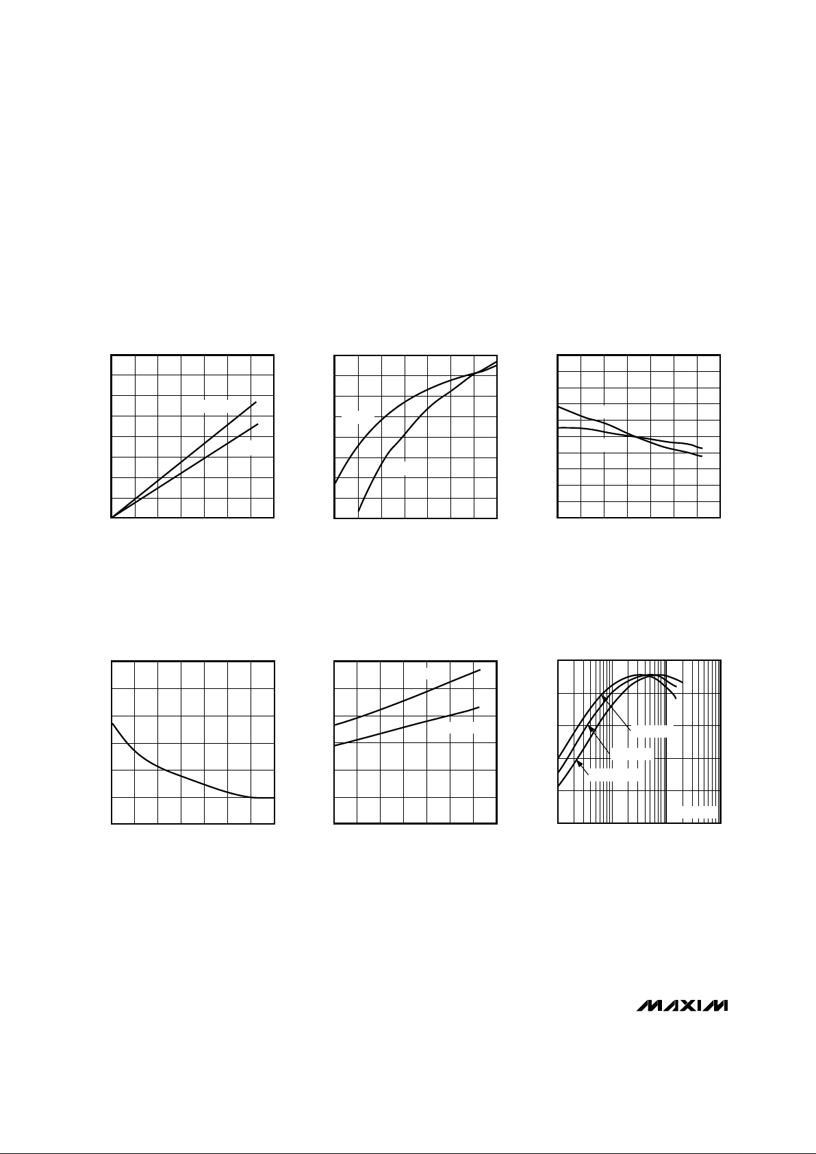
__________________________________________Typical Operating Characteristics
(All curves generated using the inverter configuration shown in the
Typical Operating Circuit
s with LV = GND, FSEL = IN or LV,
C1 = C2 = 10µF (MAX1680), C1 = C2 = 2.2µF (MAX1681), and TA= +25°C, unless otherwise noted. Test results are also valid for
the doubler configuration with LV = OUT and TA= +25°C.)
2.5
3.5
5.5
4.5
7.5
6.5
8.5
2.52.0 3.0 3.5 4.0 4.5 5.0 5.5
OUTPUT SOURCE RESISTANCE
vs. SUPPLY VOLTAGE
MAX1680/81TOC04
SUPPLY VOLTAGE (V)
OUTPUT SOURCE RESISTANCE (Ω)
0
1
3
2
5
4
6
-20-40 0 20 40 60 80 100
OUTPUT SOURCE RESISTANCE vs.
TEMPERATURE
MAX1680/81TOC05
TEMPERATURE (°C)
OUTPUT SOURCE RESISTANCE (Ω)
V
INPUT
= 3V
V
INPUT
= 5V
100
0
1 100 1000
MAX1680 EFFICIENCY vs.
LOAD CURRENT (INVERTER CONFIGURATION)
20
40
60
80
MAX1680/81TOC06
LOAD CURRENT (mA)
EFFICIENCY (%)
10
V
INPUT
= 5.5V
V
INPUT
= 4V
V
INPUT
= 3V
FSEL = IN
0
200
100
500
400
300
700
600
800
0 60 8020 40 100 120 140
OUTPUT VOLTAGE DROP
vs. LOAD CURRENT
MAX1680/81TOC01
LOAD CURRENT (mA)
OUTPUT VOLTAGE DROP (mV)
V
INPUT
= 3V
V
INPUT
= 5V
-14
-10
-12
-4
-6
-8
0
-2
2
2.0 3.5 4.02.5 3.0 4.5 5.0 5.5
OSCILLATOR FREQUENCY CHANGE
vs. SUPPLY VOLTAGE
MAX1680/81TOC02
SUPPLY VOLTAGE (V)
OSCILLATOR FREQUENCY CHANGE (%)
MAX1680
MAX1681
-10
-6
-8
-2
-4
2
0
4
8
6
10
-40 0 20-20 40 60 80 100
OSCILLATOR FREQUENCY CHANGE
vs. TEMPERATURE
MAX1680/81TOC03
TEMPERATURE (°C)
OSCILLATOR FREQUENCY CHANGE (%)
MAX1680
MAX1681

MAX1680/MAX1681
125mA, Frequency-Selectable,
Switched-Capacitor Voltage Converters
_______________________________________________________________________________________
5
100
0
1 100 1000
MAX1681 EFFICIENCY vs.
LOAD CURRENT (DOUBLER CONFIGURATION)
20
40
60
80
MAX1680/81TOC07
LOAD CURRENT (mA)
EFFICIENCY (%)
10
V
INPUT
= 5.5V
V
INPUT
= 4V
V
INPUT
= 3V
FSEL = IN
1
0
3
2
6
5
4
8
7
9
2.0 3.5 4.02.5 3.0 4.5 5.0 5.5 6.0
MAX1680 SUPPLY CURRENT vs.
SUPPLY VOLTAGE
MAX1680/81TOC08
SUPPLY VOLTAGE (V)
SUPPLY CURRENT (mA)
DOUBLER MODE
FSEL = LV
INVERTER MODE
FSEL = IN
INVERTER MODE
FSEL = LV
DOUBLER MODE
FSEL = IN
0
5
15
10
25
20
30
3.02.5 3.5 4.0 4.5 5.0 5.5 6.0
MAX1681 SUPPLY CURRENT vs.
SUPPLY VOLTAGE
MAX1680/81TOC09
SUPPLY VOLTAGE (V)
SUPPLY CURRENT (mA)
DOUBLER MODE
FSEL = LV
INVERTER MODE
FSEL = IN
INVERTER MODE
FSEL = LV
DOUBLER MODE
FSEL = IN
3
4
6
5
7
8
9
10
0 4 6 82 10 12 14 1816 20
MAX1680 OUTPUT SOURCE RESISTANCE vs.
CAPACITANCE (INVERTER CONFIGURATION)
MAX1680/81TOC10
CAPACITANCE (µF)
OUTPUT SOURCE RESISTANCE (Ω)
V
INPUT
= 3V, FSEL = LV
V
INPUT
= 5V, FSEL = LV
V
INPUT
= 3V, FSEL = IN
V
INPUT
= 5V, FSEL = IN
3
4
6
5
7
8
9
10
0 4 6 82 10 12 14 1816 20
MAX1681 OUTPUT SOURCE RESISTANCE vs.
CAPACITANCE (DOUBLER CONFIGURATION)
MAX1680/81TOC13
CAPACITANCE (µF)
OUTPUT SOURCE RESISTANCE (Ω)
V
INPUT
= 3V, FSEL = LV
V
INPUT
= 5V, FSEL = LV
V
INPUT
= 5V, FSEL = IN
V
INPUT
= 3V, FSEL = IN
3
4
6
5
7
8
9
10
0 4 6 82 10 12 14 1816 20
MAX1680 OUTPUT SOURCE RESISTANCE vs.
CAPACITANCE (DOUBLER CONFIGURATION)
MAX1680/81TOC11
CAPACITANCE (µF)
OUTPUT SOURCE RESISTANCE (Ω)
V
INPUT
= 3V, FSEL = LV
V
INPUT
= 5V, FSEL = LV
V
INPUT
= 5V, FSEL = IN
V
INPUT
= 3V, FSEL = IN
3
4
6
5
7
8
9
10
0 4 6 82 10 12 14 1816 20
MAX1681 OUTPUT SOURCE RESISTANCE vs.
CAPACITANCE (INVERTER CONFIGURATION)
MAX1680/81TOC12
CAPACITANCE (µF)
OUTPUT SOURCE RESISTANCE (Ω)
V
INPUT
= 3V, FSEL = LV
V
INPUT
= 5V, FSEL = LV
V
INPUT
= 5V, FSEL = IN
V
INPUT
= 3V, FSEL = IN
____________________________Typical Operating Characteristics (continued)
(All curves generated using the inverter configuration shown in the
Typical Operating Circuit
s with LV = GND, FSEL = IN or LV,
C1 = C2 = 10µF (MAX1680), C1 = C2 = 2.2µF (MAX1681), and TA= +25°C, unless otherwise noted. Test results are also valid for
the doubler configuration with LV = OUT and TA= +25°C.)

_______________Detailed Description
The MAX1680/MAX1681 switched-capacitor voltage
converters either invert or double the input voltage.
They have low output resistance (3.5Ω) and can deliver
up to 125mA output current. These devices operate at
one of two selectable frequencies: 125kHz/250kHz
(MAX1680) and 500kHz/1MHz (MAX1681). This provides the flexibility to optimize capacitor size, operating
supply current, and overall circuit efficiency. Frequency
selection also allows for minimizing coupling into other
sensitive circuits. These devices contain no internal
divider; the oscillator frequency equals the switching
frequency. The devices can easily be cascaded to produce a higher output voltage, or paralleled to deliver
more current.
The MAX1680/MAX1681 feature a shutdown mode that
reduces supply current to <1µA (SHDN = high). OUT,
in the inverter configuration, pulls to ground in shutdown mode. Shutdown is not available in the doubler
configuration; connect SHDN to OUT.
__________Applications Information
Voltage Inverter
A simple voltage inverter is the most common
MAX1680/MAX1681 application. It requires three external capacitors (including the input bypass capacitor)
as shown in the
Typical Operating Circuits
(inverter
configuration). Although the output is not regulated, low
output resistance produces a typical drop of only 0.44V
with a 125mA load. This low output resistance makes
the devices fairly insensitive to changes in load (see
the graphs for Output Source Resistance vs.
Temperature and Supply Voltage in the
Typical
Operating Characteristics
section).
Voltage Doubler
The MAX1680/MAX1681 can be configured as a voltage doubler with two external capacitors as shown in
the
Typical Operating Circuits
(doubler configuration).
When loaded, the output voltage drop is similar to that
of the voltage inverter. The minimum input supply range
is slightly higher than in the inverter configuration.
Calculate ripple voltage using the equation in the
Capacitor Selection
section.
Frequency Control
A frequency-control pin, FSEL, provides design flexibility. Each device has two selectable frequencies:
125kHz/250kHz (MAX1680) and 500kHz/1MHz
(MAX1681). This allows optimization of capacitor size
and supply current for a given output load. Table 1
summarizes the frequency options .
Table 1. Nominal Switching Frequencies
MAX1680/MAX1681
125mA, Frequency-Selectable,
Switched-Capacitor Voltage Converters
6 _______________________________________________________________________________________
______________________________________________________________Pin Description
Selects operating frequency. MAX1680: 250kHz when FSEL is low, 125kHz when FSEL is high. MAX1681:
1MHz when FSEL is low, 500kHz when FSEL is high.
FSEL1
Positive Charge-Pump Capacitor ConnectionCAP+2
Negative Charge-Pump Capacitor ConnectionCAP-4
Power-Supply Ground InputGND3
Logic Voltage Input. Connect LV to GND.LV6
Power-Supply Positive Voltage InputIN8
SHDN7
Negative Voltage OutputOUT5
Power-Supply Positive Voltage Input
Power-Supply Ground Connection
Connect LV to OUT.
Not available; connect to OUT.
Shutdown Input. Driving SHDN high disables the
charge pump, and the output goes to 0V. SHDN is a
CMOS input.
Positive Voltage Output
MAX1680
250FSEL = LV
125FSEL = IN
FSEL CONNECTION
MAX1681
1000
500
FREQUENCY (kHz)
INVERTER DOUBLER
PIN
FUNCTION
NAME

Operating Frequency Trade-Offs
It is important to recognize the trade-offs between
switching frequency, power consumption, noise, cost,
and performance. Higher frequency switching reduces
capacitor size while maintaining the same output
impedance, thus saving capacitor cost and board
space. Lower frequency designs use less supply current. Table 2 summarizes the relative trade-offs.
Table 2. Switching-Frequency Trade-Offs
Capacitor Selection
The MAX1680/MAX1681 are tested with capacitor values of 10µF and 2.2µF, respectively. Capacitor size
and switching speed determine output resistance.
Larger C1 values decrease the output resistance until
the internal switch resistance (3.5Ω typ) becomes the
dominant term. Low-ESR capacitors minimize output
resistance and ripple voltage. The entire circuit’s output
resistance can be approximated by the following equation:
R
OUT
≅ RO+ 4 x ESRC1+ ESRC2+ [1 / (f
OSC
x C1)] +
[1 / (f
OSC
x C2)]
where ROis the device’s internal effective switch resistance and f
OSC
is the switching frequency. Output
resistance is a critical circuit component, as it determines the voltage drop that will occur at the output from
the ideal value of -V
INPUT
(or 2V
INPUT
when doubling).
To optimize performance, minimize overall resistance in
the system. In particular, equivalent series resistance
(ESR) in the capacitors produces significant losses as
large currents flow through them. Therefore, choose a
low-ESR capacitor for highest efficiency. Table 3 lists
recommended capacitors and their suppliers.
Calculate the output ripple voltage as follows:
V
RIPPLE
= [(I
OUT
) / (2 x f
OSC
x C2)] + 2 x (I
OUT
x ESRC2)
where I
OUT
is the load current, fSis the charge pump’s
operating frequency, C2 is the output capacitor, and
ESRC2is the output capacitor’s ESR.
Table 4 lists the minimum recommended capacitances
that allow for the maximum output current. The output
capacitor, C2, is normally equal to or greater than the
charge-pump capacitor, C1. Capacitor values can be
scaled directly proportional to the input voltage, frequency, and load current. For example, for V
INPUT
=
5V, I
LOAD
= 125mA at f
OSC
= 125kHz, a 6.4µF mini-
mum capacitor is recommended. For an output of only
62.5mA, a 3.2µF capacitor is recommended. C1’s value
can be estimated as follows:
C1 = 6.4µF x (V
INPUT
/ 5.0V) x (125kHz / f
OSC
) x
(I
LOAD
/ 125mA)
where f
OSC
is the switching frequency (kHz) and I
LOAD
is the output current (mA) required.
MAX1680/MAX1681
125mA, Frequency-Selectable,
Switched-Capacitor Voltage Converters
_______________________________________________________________________________________ 7
ATTRIBUTE
C1, C2 Values Larger
LOWER
FREQUENCY
Output Ripple Larger
Smaller
Smaller
SUPPLIER
Marcon/United Chemi-Con (847) 696-2000
PHONE
AVX
(803) 946-0690
(800) 282-4975
(847) 696-9278
(803) 626-3123
HIGHER
FREQUENCY
Supply Current Smaller Larger
FAX DEVICE TYPE
Ceramic capacitors
Surface mount, TPS series
Matsuo (714) 969-2491 (714) 960-6492 Surface mount, 267 series
Nichicon
USA: (847) 843-7500
Japan: 81-7-5231-8461
USA: (847) 843-2798
Japan: 81-7-5256-4158
Sanyo
USA: (619) 661-6835
Japan: 81-7-2070-6306
USA: (619) 661-1055
Japan: 81-7-2070-1174
Through-hole, OS-CON series
Through-hole, PL series
Sprague (603) 224-1961 (603) 224-1430
TDK (847) 390-4373 (847) 390-4428 Ceramic capacitors
Surface mount, 595D series
United Chemi-Con (714) 255-9500 (714) 255-9400
Vishay/Vitramon (203) 268-6261 (203) 452-5670 SMT ceramic chip capacitors
Through-hole, LXF series
Table 3. Low-ESR Capacitor Suppliers
MAX1680/MAX1681
Bypass Capacitor
Bypass the input voltage to reduce AC impedance and
to prevent internal switching noise. Bypassing depends
on the source impedance location. The AC ripple current is 2 x I
OUT
for the doubler and the inverter. Use a
large bypass capacitor (equal to C1) if the supply has
high AC impedance.
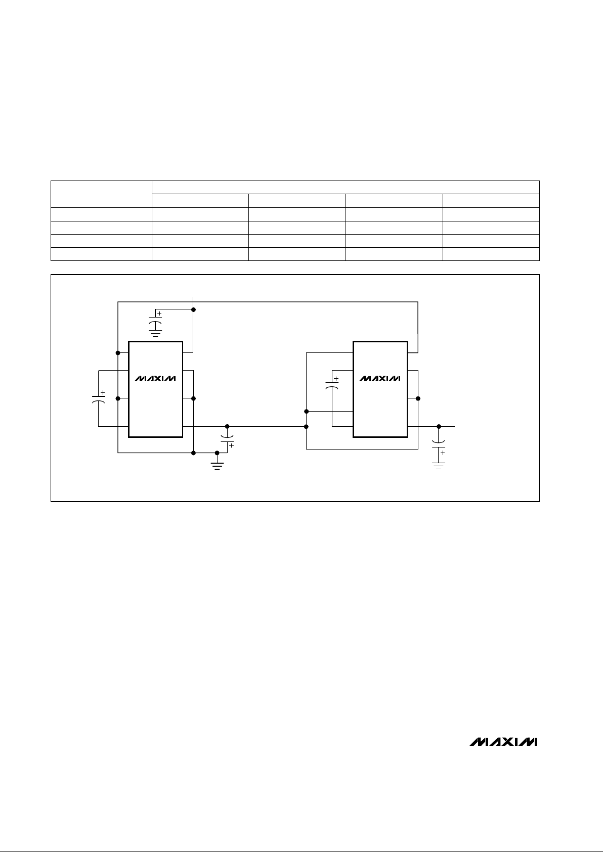
Cascading Devices
To produce larger negative voltages, cascade two
devices (Figure 1). For two devices, the unloaded output voltage is approximately -2 x V
INPUT
, but this value
is reduced slightly by the first device’s output resistance multiplied by the second device’s quiescent current. The effective output resistance for a cascaded
device is larger than that for an individual device (20Ω
for two devices). Cascading several devices increases
output resistance and reduces efficiency. If a large
negative voltage is required for several stages, an
inductive inverting switching regulator such as the
MAX629 or MAX774 may offer more advantages.
Paralleling Devices
Parallel two or more MAX1680/MAX1681s to reduce
output resistance voltage drop under a given load. With
reduced output resistance, paralleled devices deliver
higher load currents. Figure 2 shows two
MAX1680/MAX1681s connected in parallel. Output
resistance is inversely proportional to the number of
devices.
125mA, Frequency-Selectable,
Switched-Capacitor Voltage Converters
8 _______________________________________________________________________________________
250 1.2
125 2.5
1.9
3.8
500 0.6 0.9
Table 4. Minimum Recommended Capacitances for Maximum Output Current
CAPACITANCE (µF) (C1 = C2)
2.5
5.1
3.2
6.4
1.2 1.6
1000 0.3 0.4 0.6 0.8
VIN= 3V
f
OSC
(kHz)
VIN= 2V VIN= 5VVIN= 4V
MAX1681
FSEL IN
CAP+ SHDN
GND
1µF
1µF
1µF
LV
CAP- OUT
MAX1681
FSEL IN
CAP+ SHDN
GND
+V
INPUT
V
OUT
= -V
INPUT
1µF
NOTE: USE 4.7µF CAPACITORS FOR MAX1680.
1µF
LV
CAP- OUT
V
OUT
= -2V
INPUT
Figure 1. Cascading MAX1680/MAX1681s to Increase Output Voltage
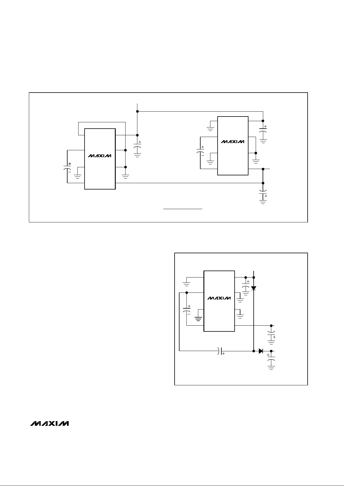
Combined Doubler and Inverter
Figure 3 shows a single MAX1680/MAX1681 as an
inverter and a doubler. The maximum output current is
the sum of the loads on the two outputs and is still limited to 125mA. As the device is loaded, the output voltages move toward ground. In this particular
configuration, connect LV to GND (inverter). The diodes
used in the circuit cause a drop of approximately 0.7V
in the doubler’s output voltage, impacting efficiency.
Compatibility with the MAX660 and
MAX860/MAX861
The MAX1680/MAX1681 can be used in place of the
MAX860/MAX861, except for the SHDN and FSEL pins.
The MAX1680/MAX1681 shut down with a high input
voltage, compared with the MAX860/MAX861. The
MAX1680/MAX1681 have only two frequency choices.
Replacing the MAX660 with the MAX1680/MAX1681
involves a wiring change, as the external oscillator pin
is replaced by the shutdown feature. Table 5 compares
the devices.
MAX1680/MAX1681
125mA, Frequency-Selectable,
Switched-Capacitor Voltage Converters
_______________________________________________________________________________________ 9
MAX1681
FSEL IN
+V
INPUT
CAP+ SHDN
GND
1µF
1µF
LV
CAP- OUT
GND
MAX1681
"n"
FSEL IN
CAP+ SHDN
1µF
1µF
1µF
V
OUT
NOTE: USE 4.7µF CAPACITORS FOR MAX1680. V
OUT
= -V
INPUT
LV
CAP- OUT
R
OUT
=
R
OUT
OF SINGLE DEVICE
NUMBER OF DEVICES (n)
Figure 2. Paralleling MAX1680/MAX1681s to Increase Output Current
MAX1681
FSEL IN
+V
INPUT
CAP+ SHDN
GND1µF
1µF
1µF
1µF
1µF
LV
CAP- OUT
V
OUT
= -V
INPUT
D1
IN4148
D2
IN4148
V
OUT
= 2V
INPUT
-V
FD1
-VFD2
NOTE: USE 4.7µF CAPACITORS FOR MAX1680.
Figure 3. Combined Doubler and Inverter
MAX1680/MAX1681
125mA, Frequency-Selectable,
Switched-Capacitor Voltage Converters
10 ______________________________________________________________________________________
LV
OUTCAP-
1
2
87IN
SHDNCAP+
GND
FSEL
SO
TOP VIEW
3
4
6
5
MAX1680
MAX1681
__________________Pin Configuration ___________________Chip Information
TRANSISTOR COUNT: 171
SUBSTRATE CONNECTED TO IN
OUTPUT
CURRENT
(mA)
PART NUMBER
MAX665 0.20/1.0
TYPICAL
QUIESCENT
CURRENT (mA)
MAX660 0.12/1.0
100
100
MAX860 0.20/0.60/1.40 50
SWITCHING
FREQUENCY
(kHz)
6.5
OUTPUT
RESISTANCE
(Ω)
6.5
5/40
5/40
12 6/50/130
MAX1680 2.5/5.0
MAX861 0.30/1.10/2.50
125
50
MAX1681 10/20 125
3.5
12
125/250
13/100/250
3.5 500/1000
ICL7660 0.080 10 55 5
Table 5. Device Comparison
MAX1680/MAX1681
125mA, Frequency-Selectable,
Switched-Capacitor Voltage Converters
______________________________________________________________________________________ 11
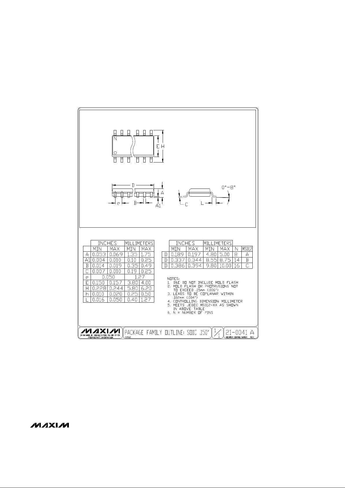
________________________________________________________Package Information
SOICN.EPS

MAX1680/MAX1681
125mA, Frequency-Selectable,
Switched-Capacitor Voltage Converters
NOTES
Maxim cannot assume responsibility for use of any circuitry other than circuitry entirely embodied in a Maxim product. No circuit patent licenses are
implied. Maxim reserves the right to change the circuitry and specifications without notice at any time.
12
____________________Maxim Integrated Products, 120 San Gabriel Drive, Sunnyvale, CA 94086 408-737-7600
© 1997 Maxim Integrated Products Printed USA is a registered trademark of Maxim Integrated Products.
 Loading...