_______________General Description
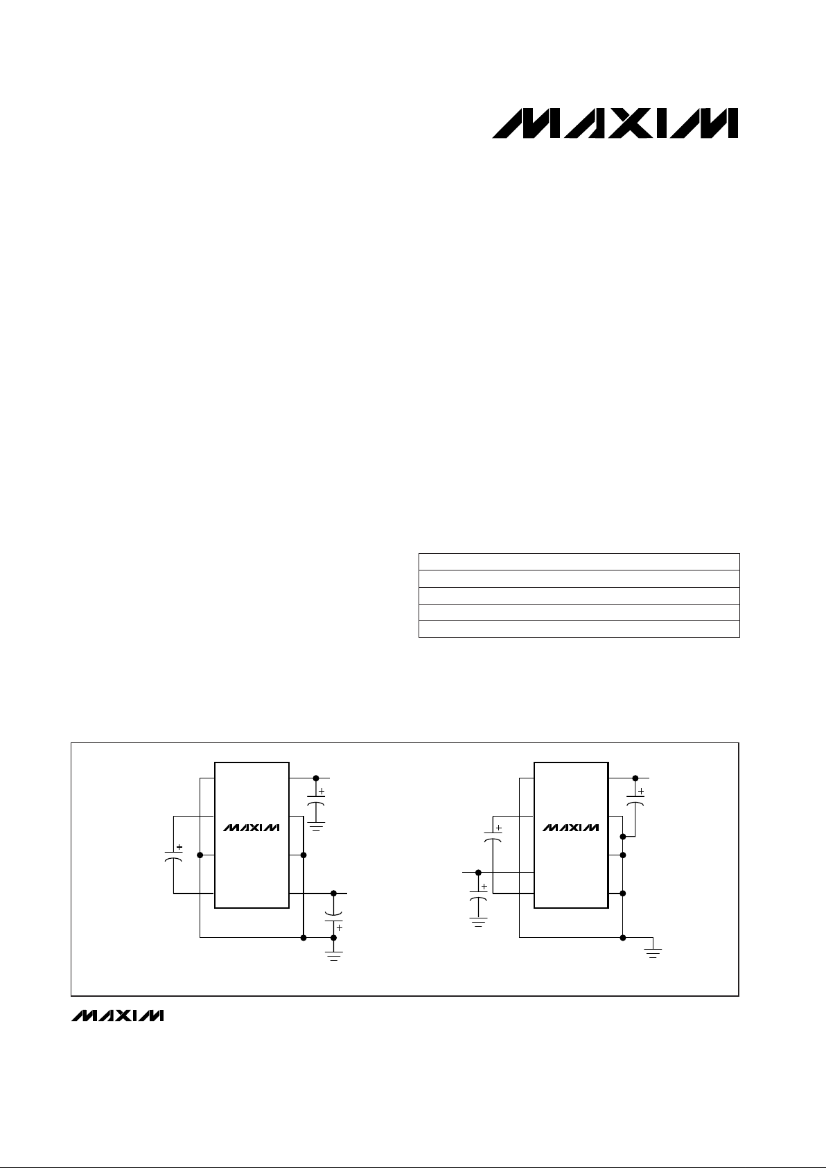
The MAX1680/MAX1681 inductorless switched-capacitor voltage converters either invert an input voltage of
+2.0V to +5.5V or double it while supplying up to
125mA output current. They have a selectable-frequency option that allows the use of small capacitors: 4.7µF
(MAX1680), 1µF (MAX1681). With their high output current capability, these charge-pump devices are suitable replacements for inductor-based regulators, which
require more expensive external components and additional board space.
The devices’ equivalent output resistance (typically
3.5Ω) allows them to deliver as much as 125mA with
only a 440mV drop. A shutdown feature reduces quiescent current to less than 1µA. The MAX1680/MAX1681
are available in 8-pin SO packages. For devices that
deliver up to 50mA in smaller µMAX packages, refer to
the MAX860/MAX861 data sheet.
________________________Applications
Local Negative Supplies
Interface Power Supplies
Op-Amp Power Supplies
MOSFET Bias
____________________________Features
♦ Selectable Switching Frequencies:
125kHz/250kHz (MAX1680)
500kHz/1MHz (MAX1681)
♦ Allow Use of Small Capacitors
(1µF for the MAX1681)
♦ 125mA Output Current
♦ 3.5Ω Output Impedance
♦ 1µA Logic-Controlled Shutdown
♦ Configurable as Voltage Inverters or Doublers
♦ +2.0V to +5.5V Input Voltage Range
♦ Available in 8-Pin SO Packages
♦ 90% Efficiency
MAX1680/MAX1681
125mA, Frequency-Selectable,
Switched-Capacitor Voltage Converters
________________________________________________________________
Maxim Integrated Products
1
MAX1681
FSEL IN
CAP+ SHDN
GND
C1
1µF
+V
INPUT
+3V TO +5.5V
INVERTED
OUTPUT
VOLTAGE
C2
1µF
1µF
LV
CAP-
INVERTER CONFIGURATION
OUT
MAX1681
FSEL IN
CAP+ SHDN
GND
C1
1µF
C2
1µF
DOUBLED
OUTPUT
VOLTAGE
+V
INPUT
+4V TO +5.5V
NOTE: USE 4.7µF CAPACITORS FOR MAX1680
INPUT VOLTAGE RANGE: +2.5V TO +5.5V.
NOTE: USE 4.7µF CAPACITORS FOR MAX1680
INPUT VOLTAGE RANGE: +2.0V TO +5.5V.
1µF
LV
CAP-
DOUBLER CONFIGURATION
OUT
__________________________________________________Typical Operating Circuits
19-1247; Rev 0; 7/97
PART
MAX1680C/D
MAX1680ESA
MAX1681C/D
0°C to +70°C
-40°C to +85°C
0°C to +70°C
TEMP. RANGE PIN-PACKAGE
Dice*
8 SO
Dice*
______________Ordering Information
*
Contact factory for dice specifications.
Pin Configuration appears at end of data sheet.
MAX1681ESA -40°C to +85°C 8 SO
For free samples & the latest literature: http://www.maxim-ic.com, or phone 1-800-998-8800.
For small orders, phone 408-737-7600 ext. 3468.

V
MAX1680/MAX1681
125mA, Frequency-Selectable,
Switched-Capacitor Voltage Converters
2 _______________________________________________________________________________________
ABSOLUTE MAXIMUM RATINGS
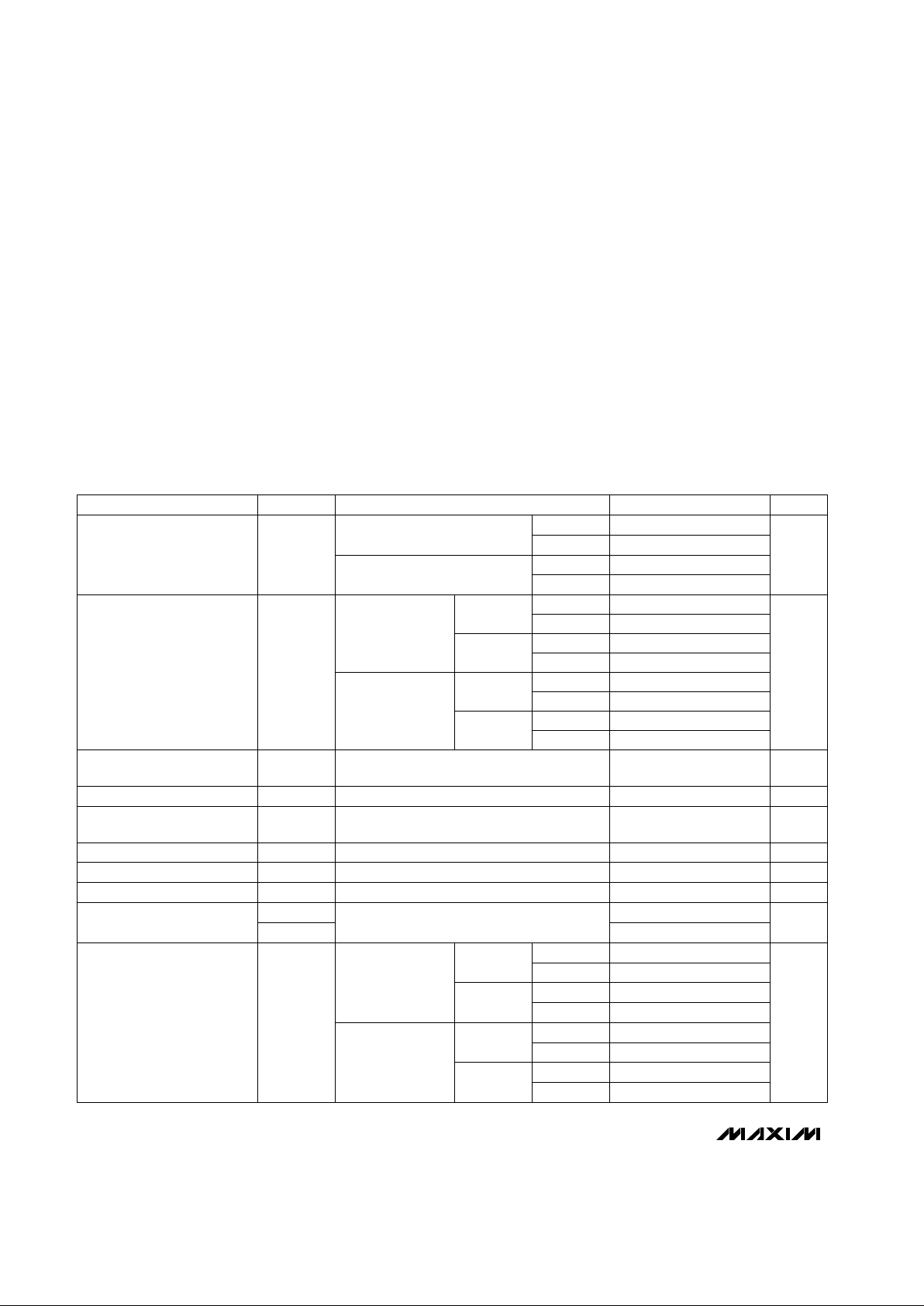
ELECTRICAL CHARACTERISTICS
(
Typical Operating Circuits
(inverter configuration), FSEL = LV = GND, VIN= 5V, C1 = C2 = 10µF (MAX1680), C1 = C2 = 2.2µF
(MAX1681), T
A
= 0°C to +85°C, unless otherwise noted. Typical values are at TA= +25°C.)
Stresses beyond those listed under “Absolute Maximum Ratings” may cause permanent damage to the device. These are stress ratings only, and functional
operation of the device at these or any other conditions beyond those indicated in the operational sections of the specifications is not implied. Exposure to
absolute maximum rating conditions for extended periods may affect device reliability.
IN..............................................................................-0.3V to +6V
LV....................................................(V
OUT
- 0.3V) to (VIN+ 0.3V)
CAP+ ...........................................................-0.3V to (V
IN
+ 0.3V)
SHDN, FSEL ......................................(V
LV
- 0.3V) to (VIN+ 0.3V)
OUT, CAP-..................................................................-6V to 0.3V
Continuous Output Current ..............................................135mA
Output Short-Circuit Duration to GND (Note 1) ...................1sec
Continuous Power Dissipation (T
A
= +70°C)
SO (derate 5.88mW/°C above +70°C)..........................471mW
Operating Temperature Range ...........................-40°C to +85°C
Junction Temperature......................................................+150°C
Storage Temperature Range.............................-65°C to +160°C
Lead Temperature (soldering, 10sec).............................+300°C
I
LOAD
= 125mA
Inverter configuration,
RL= 1kΩ, LV = GND
LV = GND (Note 3)
FSEL = IN or LV
SHDN = IN
OUT = GND, SHDN = IN
CONDITIONS
375 500 625
750 1000 1250
94 125 156
187 250 313
4V
IH
V-3.75 -4.56V
LOAD
Output Voltage Under Load
(Note 2)
V
3.0 5.5
2.0 5.5
V
1V
IL
Shutdown, FSEL Thresholds
µA-1 1I
FSEL
Input Bias Current (FSEL)
Ω3.5 10R
OUT
Output Resistance (Note 2)
Ω1 5R
OUT(SHUT)
Output Resistance to Ground
in Shutdown
µA1I+
SHDN
Shutdown Current
µA-1 1I
SHDN
Input Bias Current (SHDN)
UNITSMIN TYP MAXSYMBOLPARAMETER
Doubler configuration,
RL= 1kΩ, LV = OUT
4.0 5.5
V
IN
2.5 5.5
Input Voltage Range
MAX1680
5.4
mA
10.8
FSEL = IN
(125kHz)
FSEL = LV
(250kHz)
MAX1681
21.6
43.2
I+
FSEL = IN
(500kHz)
Supply Current
FSEL = LV
(1MHz)
Note 1: Shorting OUT to IN may damage the device and should be avoided.
TA= +25°C
TA= +25°C
TA= +25°C
TA= +25°C
MAX1681
MAX1680
MAX1681
MAX1680
TA= +25°C
TA= +25°C
TA= +25°C
TA= +25°C
2.5 4.5
5 9
10 18
20 36
FSEL = LV
157 348
FSEL = IN
MAX1680
79 174
FSEL = LV
570 1490
kHz
FSEL = IN
MAX1681
f
OSC
Switching Frequency
285 745

mA
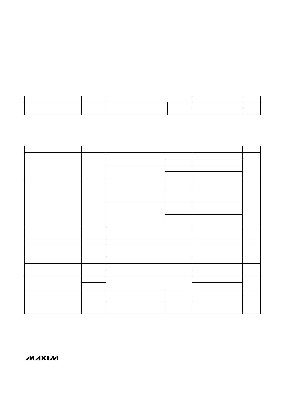
ELECTRICAL CHARACTERISTICS
(
Typical Operating Circuits
(inverter configuration), FSEL = LV = GND, VIN= 5V, C1 = C2 = 10µF (MAX1680), C1 = C2 = 2.2µF
(MAX1681), T
A
= -40°C to +85°C, unless otherwise noted.) (Note 4)
MAX1680/MAX1681
125mA, Frequency-Selectable,
Switched-Capacitor Voltage Converters
_______________________________________________________________________________________ 3
FSEL = IN
FSEL = LV
MAX1681
I
LOAD
= 125mA
21.6
mA
Inverter configuration,
RL= 1kΩ, LV = GND
43.2
Doubler configuration,
R
L
= 1kΩ, LV = OUT
MAX1681
FSEL = LV
FSEL = IN
MAX1680
LV = GND (Note 3)
FSEL = IN or LV
SHDN = IN
OUT = GND, SHDN = IN
CONDITIONS
I+
FSEL = IN
(500kHz)
Supply Current
FSEL = LV
(1MHz)
kHz
285 745
f
OSC
570 1490
79 174
157 348
Switching Frequency
4V
IH
V-3.75V
LOAD
Output Voltage Under Load
(Note 2)
3.0 5.5
V
2.0 5.5
4.0 5.5
V
IN
V
-1 1V
IL
Shutdown, FSEL Thresholds
µA-1 1I
FSEL
Input Bias Current (FSEL)
Ω10R
OUT
Output Resistance (Note 2)
Ω5R
OUT(SHUT)
Output Resistance in
Shutdown
µA1I+
SHDN
Shutdown Current
µA1I
SHDN
Input Bias Current (SHDN)
UNITSMIN TYP MAXSYMBOLPARAMETER
MAX1681
MAX1680
2.5 5.5
Input Voltage Range
MAX1681
MAX1680
MAX1680
5.4
10.8
FSEL = IN
(125kHz)
FSEL = LV
(250kHz)
ELECTRICAL CHARACTERISTICS (continued)
(
Typical Operating Circuits
(inverter configuration), FSEL = LV = GND, VIN= 5V, C1 = C2 = 10µF (MAX1680), C1 = C2 = 2.2µF
(MAX1681), T
A
= 0°C to +85°C, unless otherwise noted. Typical values are at TA= +25°C.)
Note 2: C1 and C2 are low-ESR (<0.2Ω) capacitors. Capacitor ESR adds to the circuit’s output resistance. Using capacitors with
higher ESR reduces output voltage and efficiency. The specified output resistance includes the C1 and C2 0.2Ω ESR.
Note 3: The typical threshold for V
INPUT
other than +5V is 0.35V
INPUT(VIL
= VIH).
Note 4: Specifications to -40°C are guaranteed by design, not production tested.
RL= 100Ω to GND, FSEL = IN
MAX1680
MAX1681
%
80
90
Power Efficiency
UNITSMIN TYP MAXSYMBOLPARAMETER CONDITIONS

MAX1680/MAX1681
125mA, Frequency-Selectable,
Switched-Capacitor Voltage Converters
4 _______________________________________________________________________________________
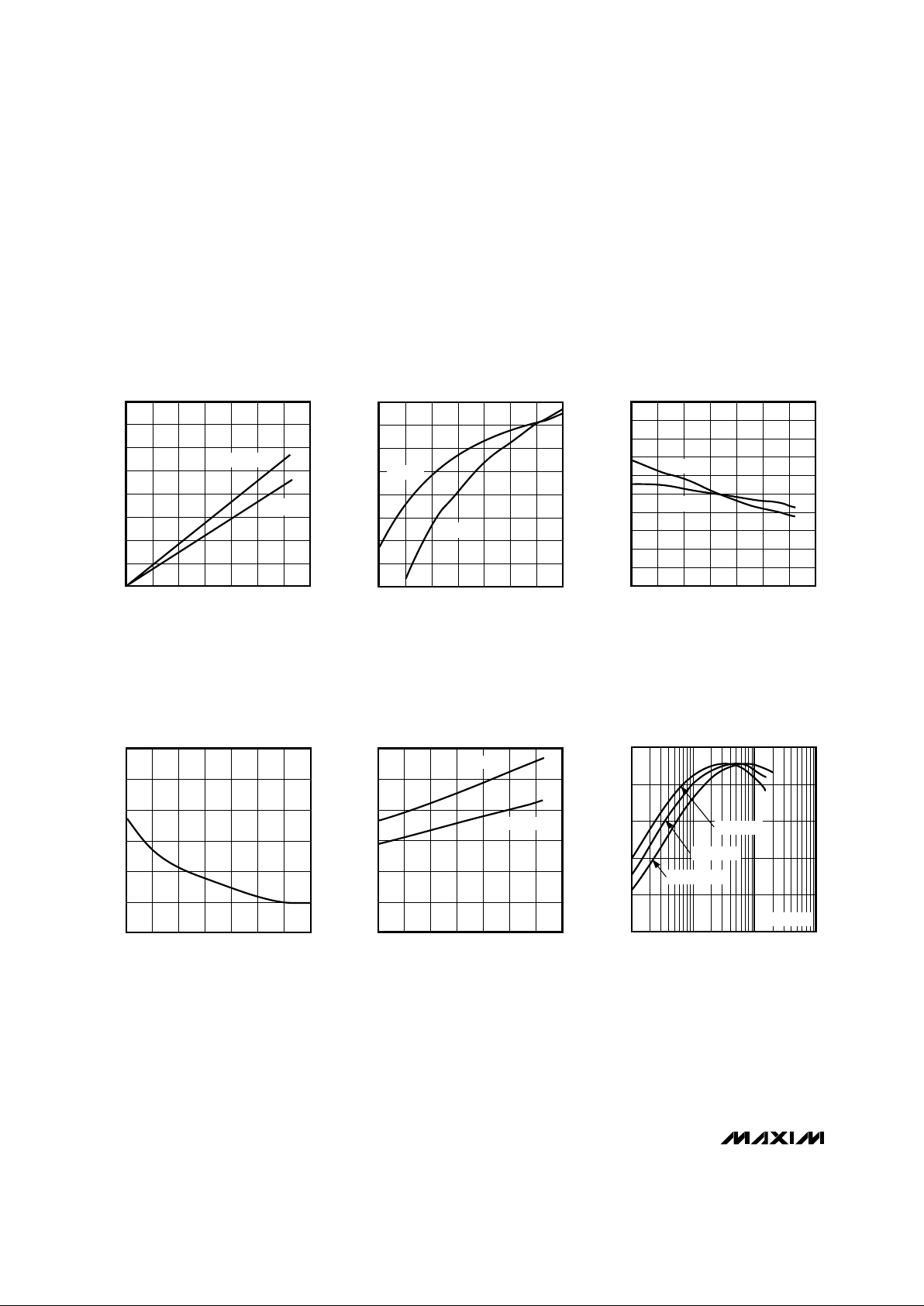
__________________________________________Typical Operating Characteristics
(All curves generated using the inverter configuration shown in the
Typical Operating Circuit
s with LV = GND, FSEL = IN or LV,
C1 = C2 = 10µF (MAX1680), C1 = C2 = 2.2µF (MAX1681), and TA= +25°C, unless otherwise noted. Test results are also valid for
the doubler configuration with LV = OUT and TA= +25°C.)
2.5
3.5
5.5
4.5
7.5
6.5
8.5
2.52.0 3.0 3.5 4.0 4.5 5.0 5.5
OUTPUT SOURCE RESISTANCE
vs. SUPPLY VOLTAGE
MAX1680/81TOC04
SUPPLY VOLTAGE (V)
OUTPUT SOURCE RESISTANCE (Ω)
0
1
3
2
5
4
6
-20-40 0 20 40 60 80 100
OUTPUT SOURCE RESISTANCE vs.
TEMPERATURE
MAX1680/81TOC05
TEMPERATURE (°C)
OUTPUT SOURCE RESISTANCE (Ω)
V
INPUT
= 3V
V
INPUT
= 5V
100
0
1 100 1000
MAX1680 EFFICIENCY vs.
LOAD CURRENT (INVERTER CONFIGURATION)
20
40
60
80
MAX1680/81TOC06
LOAD CURRENT (mA)
EFFICIENCY (%)
10
V
INPUT
= 5.5V
V
INPUT
= 4V
V
INPUT
= 3V
FSEL = IN
0
200
100
500
400
300
700
600
800
0 60 8020 40 100 120 140
OUTPUT VOLTAGE DROP
vs. LOAD CURRENT
MAX1680/81TOC01
LOAD CURRENT (mA)
OUTPUT VOLTAGE DROP (mV)
V
INPUT
= 3V
V
INPUT
= 5V
-14
-10
-12
-4
-6
-8
0
-2
2
2.0 3.5 4.02.5 3.0 4.5 5.0 5.5
OSCILLATOR FREQUENCY CHANGE
vs. SUPPLY VOLTAGE
MAX1680/81TOC02
SUPPLY VOLTAGE (V)
OSCILLATOR FREQUENCY CHANGE (%)
MAX1680
MAX1681
-10
-6
-8
-2
-4
2
0
4
8
6
10
-40 0 20-20 40 60 80 100
OSCILLATOR FREQUENCY CHANGE
vs. TEMPERATURE
MAX1680/81TOC03
TEMPERATURE (°C)
OSCILLATOR FREQUENCY CHANGE (%)
MAX1680
MAX1681
 Loading...