

General Description
The MAX16801A/B/MAX16802A/B high-brightness (HB)
LED driver-control ICs contain all the circuitry required
for the design of wide-input-voltage-range LED drivers
for general lighting and display applications. The
MAX16801 is well suited for universal input (rectified
85VAC to 265VAC) LED drivers, while the MAX16802 is
intended for low-input-voltage (10.8VDC to 24VDC) LED
drivers.
When the LED current needs to be tightly regulated, an
additional on-board error amplifier with 1% accurate reference can be utilized. A wide dimming range can be
implemented by using low-frequency PWM dimming.
The MAX16801/MAX16802 feature an input undervoltage
lockout (UVLO) for programming the input-supply start
voltage, and to ensure proper operation during brownout
conditions. The MAX16801 has an internal-bootstrap
undervoltage lockout circuit with a large hysteresis that
simplifies offline LED driver designs. The MAX16802 does
not have this internal bootstrap circuit and can be biased
directly from a +12V rail.
The 262kHz fixed switching frequency is internally
trimmed, allowing for optimization of the magnetic and filter components, resulting in a compact, cost-effective
LED driver. The MAX16801A/MAX16802A are offered with
50% maximum duty cycle. The MAX16801B/MAX16802B
are offered with 75% maximum duty cycle. These devices
are available in an 8-pin µMAX
®
package and operate
over the -40°C to +85°C temperature range.
Applications
Features
♦ Suitable for Buck, Boost, Flyback, SEPIC, and
Other Topologies
♦ Up to 50W or Higher Output Power
♦ Universal Offline Input Voltage Range: Rectified
85VAC to 265VAC (MAX16801)
♦ IN Pin Directly Driven From 10.8VDC to 24VDC
Input (MAX16802)
♦ Internal Error Amplifier with 1% Accurate
Reference for Precise LED Current Regulation
♦ PWM or Linear Dimming
♦ Fixed Switching Frequency of 262kHz ±12%
♦ Thermal Shutdown
♦ Digital Soft-Start
♦ Programmable Input Startup Voltage
♦ Internal Bootstrap UVLO with Large Hysteresis
(MAX16801)
♦ 45µA (typ) Startup Supply Current, 1.4mA (typ)
Operating Supply Current
♦ 50% (MAX16801A/MAX16802A) or 75%
(MAX16801B/MAX16802B) Maximum Duty Cycle
♦ Available in a Tiny 8-Pin µMAX Package
MAX16801A/B/MAX16802A/B
Offline and DC-DC PWM Controllers for
High-Brightness LED Drivers
________________________________________________________________ Maxim Integrated Products 1
Ordering Information
19-3880; Rev 1; 1/06
For pricing, delivery, and ordering information, please contact Maxim/Dallas Direct! at
1-888-629-4642, or visit Maxim’s website at www.maxim-ic.com.
PART
TEMP
RANGE
PINPACKAGE
MAX16801AEUA+ -40°C to +85°C 8 µMAX
MAX16801BEUA+ -40°C to +85°C 8 µMAX
MAX16802AEUA+ -40°C to +85°C 8 µMAX
MAX16802BEUA+ -40°C to +85°C 8 µMAX
+Denotes lead-free package.
Offline and DC-DC LED
Drivers
RGB Back Light for LCD
TVs and Monitors
Commercial and
Industrial Lighting
Decorative and
Architectural Lighting
EVALUATION KIT
AVAILABLE
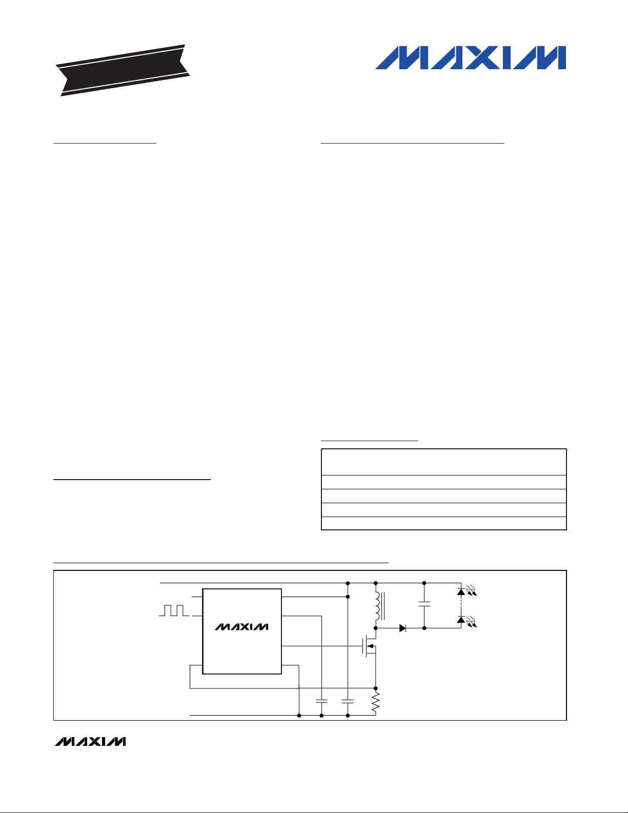
Q1
MAX16802B
10.8VDC TO 24VDC
PWM
GND
C1 R1
L1
D1
C2
C3
LEDs
CS
COMP
DIM/FB
UVLO/EN IN
VCC
NDRV
GND
ENABLE
Typical Operating Circuit
Warning: The MAX16801/MAX16802 are designed to work with high voltages. Exercise caution.
µMAX is a registered trademark of Maxim Integrated Products, Inc.
MAX16801A/B/MAX16802A/B
Offline and DC-DC PWM Controllers for
High-Brightness LED Drivers
2 _______________________________________________________________________________________
ABSOLUTE MAXIMUM RATINGS
ELECTRICAL CHARACTERISTICS
(VIN= +12V (MAX16801: VINmust first be brought up to +23.6V for startup), 10nF bypass capacitors at IN and VCC, C
NDRV
= 0,
V
UVLO
= +1.4V, V
DIM/FB
= +1.0V, COMP = unconnected, VCS= 0V, TA= -40°C to +85°C, unless otherwise noted. Typical values are
at T
A
= +25°C.) (Note 1)
Stresses beyond those listed under “Absolute Maximum Ratings” may cause permanent damage to the device. These are stress ratings only, and functional
operation of the device at these or any other conditions beyond those indicated in the operational sections of the specifications is not implied. Exposure to
absolute maximum rating conditions for extended periods may affect device reliability.
IN to GND
..........................................................................
-0.3V to +30V
VCC to GND
.....................................................................
-0.3V to +13V
DIM/FB, COMP, UVLO, CS to GND..........................-0.3V to +6V
NDRV to GND.............................................-0.3V to (V
CC
+ 0.3V)
Continuous Power Dissipation (TA = +70°C)
8-Pin µMAX (derate 4.5mW/°C above +70°C) ..............362mW
Operating Temperature Range ...........................-40°C to +85°C
Storage Temperature Range ............................-65°C to +150°C
Junction Temperature......................................................+150°C
Lead Temperature (soldering, 10s) .................................+300°C
PARAMETER
CONDITIONS
UNDERVOLTAGE LOCKOUT/STARTUP
Bootstrap UVLO Wake-Up Level
V
SUVR
VIN rising (MAX16801 only)
V
Bootstrap UVLO Shutdown Level
V
SUVF
VIN falling (MAX16801 only)
V
UVLO/EN Wake-Up Threshold V
ULR2
UVLO/EN rising
V
UVLO/EN Shutdown Threshold V
ULF2
UVLO/EN falling
V
UVLO/EN Input Current I
UVLO
TJ = +125°C 25 nA
UVLO/EN Hysteresis 50 mV
IN Supply Current In
Undervoltage Lockout
I
START
VIN = +19V, for MAX16801 only when in
bootstrap UVLO
45 90 µA
IN Voltage Range V
IN
24 V
t
EXTR
UVLO/EN steps up from +1.1V to +1.4V 12
UVLO/EN Propagation Delay
t
EXTF
UVLO/EN steps down from +1.4V to +1.1V 1.8
µs
t
BUVR
VIN steps up from +9V to +24V 5
Bootstrap UVLO Propagation
Delay
t
BUVF
VIN steps down from +24V to +9V 1
µs
INTERNAL SUPPLY
VCC Regulator Set Point V
CCSP
VIN = +10.8V to +24V, sinking 1µA to 20mA
from V
CC
7
V
IN Supply Current After Startup I
IN
VIN = +24V 1.4 2.5 mA
Shutdown Supply Current UVLO/EN = low 90 µA
GATE DRIVER
)
Measured at NDRV sinking, 100mA 2 4
Driver Output Impedance
)
Measured at NDRV sourcing, 20mA 4 12
Ω
Driver Peak Sink Current 1A
Driver Peak Source Current
A
PWM COMPARATOR
Comparator Offset Voltage
V
COMP
- V
CS
V
CS Input Bias Current I
CS
VCS = 0V -2 +2 µA
Comparator Propagation Delay t
PWM
VCS = +0.1V 60 ns
Minimum On-Time
)
ns
SYMBOL
MIN TYP MAX UNITS
19.68 21.6 23.60
9.05 9.74 10.43
1.188 1.28 1.371
1.168 1.23 1.291
R
ON(LOW
R
ON(HIGH
VO
PWM
t
ON(MIN
10.8
1.15 1.38 1.70
10.5
0.65
150
MAX16801A/B/MAX16802A/B
Offline and DC-DC PWM Controllers for
High-Brightness LED Drivers
_______________________________________________________________________________________ 3
Note 1: All devices are 100% tested at TA= +85°C. All limits over temperature are guaranteed by characterization.
Note 2: V
REF
is measured with DIM/FB connected to the COMP pin (see the Functional Diagram).
Note 3: The MAX16801 is intended for use in universal input offline drivers. The internal clamp circuit is used to prevent the boot-
strap capacitor (C1 in Figure 5) from charging to a voltage beyond the absolute maximum rating of the device when
EN/UVLO is low. The maximum current to IN (hence to clamp) when UVLO is low (device in shutdown), must be externally
limited to 2mA (max). Clamp currents higher than 2mA may result in clamp voltage higher than +30V, thus exceeding the
absolute maximum rating for IN. For the MAX16802, do not exceed the +24V maximum operating voltage of the device.
ELECTRICAL CHARACTERISTICS (continued)
(VIN= +12V (MAX16801: VINmust first be brought up to +23.6V for startup), 10nF bypass capacitors at IN and VCC, C
NDRV
= 0,
V
UVLO
= +1.4V, V
DIM/FB
= +1.0V, COMP = unconnected, VCS= 0V, TA= -40°C to +85°C, unless otherwise noted. Typical values are
at T
A
= +25°C.) (Note 1)
PARAMETER
CONDITIONS
CURRENT-SENSE COMPARATOR
Current-Sense Trip Threshold V
CS
320 mV
CS Input Bias Current I
CS
VCS = 0V -2 +2 µA
Propagation Delay From
Comparator Input to NDRV
t
PWM
50mV overdrive 60 ns
Switching Frequency f
SW
290 kHz
MAX1680_A 50
Maximum Duty Cycle D
MAX
MAX1680_B 75 76
%
IN CLAMP VOLTAGE
IN Clamp Voltage V
INC
2mA sink current, MAX16801 only (Note 3)
V
ERROR AMPLIFIER
Voltage Gain R
LOAD
= 100kΩ 80 dB
Unity-Gain Bandwidth R
LOAD
= 100kΩ, C
LOAD
= 200pF 2
Phase Margin R
LOAD
= 100kΩ, C
LOAD
= 200pF 65
DIM/FB Input Offset Voltage 3mV
High 2.2 3.5
COMP Clamp Voltage
Low 0.4 1.1
V
Source Current 0.5 mA
Sink Current 0.5 mA
Reference Voltage V
REF
(Note 2)
V
Input Bias Current 50 nA
COMP Short-Circuit Current 8mA
THERMAL SHUTDOWN
Thermal-Shutdown Temperature
°C
Thermal Hysteresis 25 °C
DIGITAL SOFT-START
Soft-Start Duration
clock
Reference Voltage Steps During
Soft-Start
31
Reference Voltage Step 40 mV
SYMBOL
MIN TYP MAX UNITS
262 291
230 262
50.5
24.1 26.1 29.0
1.218 1.230 1.242
130
15,872
MHz
degrees
cycles
steps
MAX16801A/B/MAX16802A/B
Offline and DC-DC PWM Controllers for
High-Brightness LED Drivers
4 _______________________________________________________________________________________
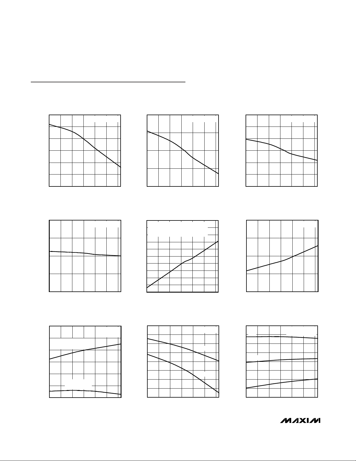
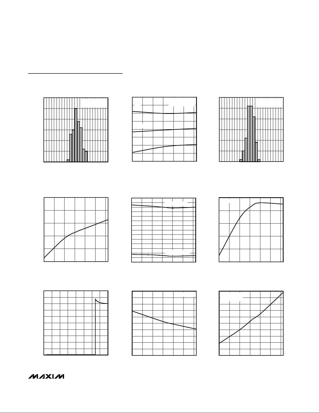
Typical Operating Characteristics
(V
UVLO/EN
= +1.4V, VFB= +1V, COMP = unconnected, VCS= 0V, TA= +25°C, unless otherwise noted.)
BOOTSTRAP UVLO WAKE-UP LEVEL
vs. TEMPERATURE
MAX16801 toc01
TEMPERATURE (°C)
V
IN
(V)
6040200-20
21.35
21.40
21.45
21.50
21.55
21.60
21.30
-40 80
MAX16801 VIN RISING
BOOTSTRAP UVLO SHUTDOWN LEVEL
vs. TEMPERATURE
MAX16801 toc02
TEMPERATURE (°C)
V
IN
(V)
6040200-20
9.8
9.9
10.0
10.1
9.7
-40 80
MAX16801 VIN FALLING
UVLO/EN WAKE-UP THRESHOLD
vs. TEMPERATURE
MAX16801 toc03
TEMPERATURE (°C)
UVLO/EN (V)
6040200-20
1.255
1.260
1.265
1.270
1.275
1.280
1.250
-40 80
UVLO/EN RISING
UVLO/EN SHUTDOWN THRESHOLD
vs. TEMPERATURE
MAX16801 toc04
TEMPERATURE (°C)
UVLO/EN (V)
6040200-20
1.15
1.20
1.25
1.30
1.10
-40 80
UVLO/EN FALLING
VIN SUPPLY CURRENT IN UNDERVOLTAGE
LOCKOUT vs. TEMPERATURE
MAX16801 toc05
TEMPERATURE (°C)
I
START
(µA)
6040200-20
43
44
45
46
47
48
49
50
51
52
42
-40 80
VIN = 19V
MAX16801 WHEN IN BOOTSTRAP UVLO
MAX16802 WHEN UVLO/EN IS LOW
VIN SUPPLY CURRENT AFTER STARTUP
vs. TEMPERATURE
MAX16801 toc06
TEMPERATURE (°C)
I
IN
(mA)
6040200-20
1.2
1.3
1.4
1.5
1.1
-40 80
VIN = 24V
VCC REGULATOR SET POINT
vs. TEMPERATURE
MAX16801 toc07
TEMPERATURE (°C)
V
CC
(V)
6040200-20
9.3
9.5
9.4
9.7
9.6
9.8
9.2
-40 80
VIN = 19V
NO LOAD
NDRV OUTPUT IS NOT
SWITCHING, V
FB
= 1.5V
NDRV OUTPUT IS
SWITCHING
VCC REGULATOR SET POINT
vs. TEMPERATURE
MAX116801 toc08
TEMPERATURE (°C)
V
CC
(V)
6040200-20
8.2
8.5
8.6
8.4
8.3
8.8
8.7
8.9
8.1
-40 80
VIN = 10.8V
10mA LOAD
20mA LOAD
CURRENT-SENSE THRESHOLD
vs. TEMPERATURE
MAX16801 toc09
TEMPERATURE (°C)
CURRENT-SENSE THRESHOLD (µV)
6040200-20
275
290
295
285
280
305
300
310
270
-40 80
+3σ
-3σ
MEAN
TOTAL NUMBER OF
DEVICES = 100
MAX16801A/B/MAX16802A/B
Offline and DC-DC PWM Controllers for
High-Brightness LED Drivers
_______________________________________________________________________________________ 5
CURRENT-SENSE THRESHOLD
MAX16801 toc10
CURRENT-SENSE THRESHOLD (mV)
PERCENTAGE OF UNITS (%)
310300290280270
5
10
15
20
25
30
0
260 320
TOTAL NUMBER OF
DEVICES = 200
SWITCHING FREQUENCY
vs. TEMPERATURE
MAX16801 toc11
TEMPERATURE (°C)
SWITCHING FREQUENCY (kHz)
6040200-20
245
260
265
255
250
275
270
280
240
-40 80
+3σ
-3σ
MEAN
TOTAL NUMBER OF
DEVICES = 100
SWITCHING FREQUENCY
MAX16801 toc12
SWITCHING FREQUENCY (kHz)
PERCENTAGE OF UNITS (%)
280270260250240
5
10
15
20
25
30
0
230 290
TOTAL NUMBER OF
DEVICES = 200
PROPAGATION DELAY FROM
CURRENT-SENSE COMPARATOR INPUT
TO NDRV vs. TEMPERATURE
MAX16801 toc13
TEMPERATURE (°C)
t
PWM
(ns)
6040200-20
55
60
65
70
75
50
-40 80
UVLO/EN PROPAGATION DELAY
vs. TEMPERATURE
MAX16801 toc14
TEMPERATURE (°C)
UNDERVOLTAGE LOCKOUT DELAY (µs)
6040200-20
4
3
2
1
7
6
5
13
12
11
10
9
8
14
0
-40 80
UVLO/EN RISING
UVLO/EN FALLING
REFERENCE VOLTAGE
vs. TEMPERATURE
MAX16801 toc15
TEMPERATURE (°C)
REFERENCE VOLTAGE (V)
6040200-20
1.226
1.227
1.228
1.229
1.230
1.225
-40 80
VIN = 12V
INPUT CURRENT
vs. INPUT CLAMP VOLTAGE
MAX16801 toc16
INPUT VOLTAGE (V)
INPUT CURRENT (mA)
27.525.020.0 22.515.0 17.512.5
1
2
3
4
5
6
7
8
9
10
0
10.0 30.0
INPUT CLAMP VOLTAGE
vs. TEMPERATURE
MAX16801 toc17
TEMPERATURE (°C)
INPUT CLAMP VOLTAGE (V)
6040200-20
25.2
25.4
25.6
25.8
26.0
26.2
26.4
26.6
26.8
27.0
25.0
-40 80
IIN = 2mA
NDRV OUTPUT IMPEDANCE
vs. TEMPERATURE
MAX16801 toc18
TEMPERATURE (°C)
R
ON
(Ω)
6040200-20
1.3
1.4
1.5
1.6
1.7
1.8
1.9
2.0
2.1
2.2
1.2
-40 80
VIN = 24V
SINKING 100mA
Typical Operating Characteristics (continued)
(V
UVLO/EN
= +1.4V, VFB= +1V, COMP = unconnected, VCS= 0V, TA= +25°C, unless otherwise noted.)

MAX16801A/B/MAX16802A/B
Detailed Description
The MAX16801/MAX16802 family of devices is intended for constant current drive of high-brightness (HB)
LEDs used in general lighting and display applications.
They are specifically designed for use in isolated and
nonisolated circuit topologies such as buck, boost, flyback, and SEPIC, operating in continuous or discontinuous mode. Current mode control is implemented with
an internally trimmed, fixed 262kHz switching frequency. A bootstrap UVLO with a large hysteresis (11.9V),
very low startup current, and low operating current
result in an efficient universal-input LED driver. In addition to the internal bootstrap UVLO, these devices also
offer programmable input startup voltage programmed
through the UVLO/EN pin. The MAX16801 is well suited
for universal AC input (rectified 85VAC to 265VAC) drivers. The MAX16802 is well suited for low input voltage
(10.8VDC to 24VDC) applications.
The MAX16801/MAX16802 regulate the LED current by
monitoring current through the external MOSFET cycle
by cycle.
Offline and DC-DC PWM Controllers for
High-Brightness LED Drivers
6 _______________________________________________________________________________________
Pin Description
NDRV OUTPUT IMPEDANCE
vs. TEMPERATURE
MAX16801 toc19
TEMPERATURE (°C)
R
ON
(Ω)
6040200-20
3.2
3.4
3.6
3.8
4.0
4.2
4.4
4.6
4.8
5.0
3.0
-40 80
VIN = 24V
SOURCING 20mA
ERROR-AMPLIFIER OPEN-LOOP GAIN
AND PHASE vs. FREQUENCY
MAX16801 toc20
FREQUENCY (Hz)
GAIN (dB)
10M1M10k1k 100k10 1001
-80
-60
-20
-40
0 -70
20
60
40
80
100
120
-100
PHASE (DEGREES)
-150
-130
-90
-110
-50
-10
-30
10
30
50
-170
0.1 100M
GAIN
PHASE
Typical Operating Characteristics (continued)
(V
UVLO/EN
= +1.4V, VFB= +1V, COMP = unconnected, VCS= 0V, TA= +25°C, unless otherwise noted.)
PIN NAME FUNCTION
1 UVLO/EN
Externally Programmable Undervoltage Lockout. UVLO programs the input start voltage. Connect
UVLO to GND to disable the device.
2 DIM/FB Low-Frequency PWM Dimming Input/Error-Amplifier Inverting Input
3 COMP
Error-Amplifier Output. Connect the compensation components between DIM/FB and COMP in highaccuracy LED current regulation.
4CS
Current-Sense Connection for Current Regulation. Connect to high side of sense resistor. An RC filter
may be necessary to eliminate leading-edge spikes.
5 GND Power-Supply Ground
6 NDRV External n-Channel MOSFET Gate Connection
7 VCC
Gate-Drive Supply. Internally regulated down from IN. Decouple with a 10nF or larger capacitor to GND.
8IN
IC Supply. Decouple with a 10nF or larger capacitor to GND. For bootstrapped operation (MAX16801),
connect a startup resistor from the input supply line to IN. Connect the bias winding supply to this point
(see Figure 5). For the MAX16802, connect IN directly to a +10.8V to +24V supply.

When in the bootstrapped mode with a transformer
(Figure 5), the circuit is protected against most output
short-circuit faults when the tertiary voltage drops
below +10V, causing the UVLO to turn off the gate
drive of the external MOSFET. This re-initiates a startup
sequence with soft-start.
When the LED current needs to be tightly regulated, an
internal error amplifier with 1% accurate reference can
be used (Figure 9). This additional feedback minimizes
the impact of passive circuit component variations and
tolerances, and can be implemented with a minimum
number of additional external components.
A wide dimming range can be implemented using a
low-frequency PWM dimming signal fed directly to the
DIM/FB pin.
LED driver circuits designed with the MAX16801 use a
high-value startup resistor R1 that charges a reservoir
capacitor C1 (Figure 5 or Figure 9). During this initial
period, while the voltage is less than the internal bootstrap UVLO threshold, the device typically consumes
only 45µA of quiescent current. This low startup current
and the large bootstrap UVLO hysteresis help minimize
the power dissipation across R1, even at the high end
of the universal AC input voltage.
An internal shutdown circuit protects the device whenever the junction temperature exceeds +130°C (typ).
Dimming
Linear dimming can be implemented by creating a
summing node at CS, as shown in Figures 6 and 7.
Low-frequency PWM (chopped-current) dimming is
possible by applying an inverted-logic PWM signal to
the DIM/FB pin of the IC (Figure 8). This might be a preferred way of dimming in situations where it is critical to
retain the light spectrum unchanged. It is accomplished by keeping constant the amplitude of the
chopped LED current.
MAX16801/MAX16802 Biasing
Implement bootstrapping from the transformer when it
is present (Figure 5). Biasing can also be realized
directly from the LEDs in non-isolated topologies
(Figure 1).
Bias the MAX16802 directly from the input voltage of
10.8VDC to 24VDC. The MAX16802 can also be used
MAX16801A/B/MAX16802A/B
Offline and DC-DC PWM Controllers for
High-Brightness LED Drivers
_______________________________________________________________________________________ 7
MAX16801B
AC
IN
BRIDGE
RECTIFIER
C1
R1
R5
R6
R2
Q1
R3
R4
C4
D3
L1
VCC NDRV
COMP
DIM/FB
UVLO/EN
IN GND
C2 C3
CS
TOTAL LED VOLTAGE:
11V TO 23V
Figure 1. Biasing the IC using LEDs in Nonisolated Flyback Driver

in applications with higher input DC voltages by implementing resistor-Zener bias (Figure 2a) or transistorZener-resistor bias (Figure 2b).
MAX16801/MAX16802 Undervoltage
Lockout
The MAX16801/MAX16802 have an input voltage
UVLO/EN pin. The threshold of this UVLO is +1.28V.
Before any operation can commence, the voltage on
this pin has to exceed +1.28V. The UVLO circuit keeps
the CPWM comparator, ILIM comparator, oscillator,
and output driver in shutdown to reduce current consumption (see the Functional Diagram). Use this UVLO
function to program the input start voltage. Calculate
the divider resistor values, R2 and R3 (Figure 5), by
using the following formulas:
The value of R3 is calculated to minimize the voltagedrop error across R2 as a result of the input bias current of the UVLO/EN pin. V
ULR2
= +1.28V, I
UVLO
=
50nA (max), VINis the value of the input-supply voltage
where the power supply must start.
where I
UVLO
is the UVLO/EN pin input current, and
V
ULR2
is the UVLO/EN wake-up threshold.
MAX16801 Bootstrap Undervoltage
Lockout
In addition to the externally programmable UVLO function offered in both the MAX16801/MAX16802, the
MAX16801 has an additional internal bootstrap UVLO
that is very useful when designing high-voltage LED
drivers (see the Functional Diagram). This allows the
device to bootstrap itself during initial power-up. The
MAX16801 attempts to start when VINexceeds the
bootstrap UVLO threshold of +23.6V. During startup,
the UVLO circuit keeps the CPWM comparator, ILIM
comparator, oscillator, and output driver shut down to
reduce current consumption. Once VINreaches
+23.6V, the UVLO circuit turns on both the CPWM and
ILIM comparators, as well as the oscillator, and allows
the output driver to switch. If VINdrops below +9.7V,
the UVLO circuit will shut down the CPWM comparator,
ILIM comparator, oscillator, and output driver thereby
returning the MAX16801 to the startup mode.
MAX16801 Startup Operation
In isolated LED driver applications, VINcan be derived
from a tertiary winding of a transformer. However, at
startup there is no energy delivered through the transformer. Therefore, a special bootstrap sequence is
required. Figure 3 shows the voltages on IN and VCC
during startup. Initially, both V
IN
and VCCare 0V. After
the line voltage is applied, C1 charges through the
startup resistor R1 to an intermediate voltage. At this
point, the internal regulator begins charging C2 (see
Figure 5). The MAX16801 uses only 45µA of the current
supplied by R1, and the remaining input current
charges C1 and C2. The charging of C2 stops when
the VCC voltage reaches approximately +9.5V, while
the voltage across C1 continues rising until it reaches
R
VV
V
R
IN ULR
ULR
23
2
2
=×
−
R
VV
IVV
ULR IN
UVLO IN ULR
3
500
2
2
≅
×
×
()
−
MAX16801A/B/MAX16802A/B
Offline and DC-DC PWM Controllers for
High-Brightness LED Drivers
8 _______________________________________________________________________________________
IN
VDC
R
D
(a)
MAX16802A
IN
VDC
Q
R
DC
(b)
MAX16802A
Figure 2. (a) Resistor-Zener and (b) Transistor-Zener-Resistor Bias Arrangements

the wake-up level of +23.6V. Once VINexceeds the
bootstrap UVLO threshold, NDRV begins switching the
MOSFET and transfers energy to the secondary and
tertiary outputs. If the voltage on the tertiary output
builds to a value higher than +9.7V (the bootstrap
UVLO lower threshold), then startup has been accomplished and sustained operation commences.
If VINdrops below +9.7V before startup is complete,
the device goes back to low-current UVLO. In this
case, increase C1 in order to store enough energy to
allow for the voltage at the tertiary winding to build up.
Soft-Start
The MAX16801/MAX16802 soft-start feature allows the
LED current to ramp up in a controlled manner. Softstart begins after UVLO deasserts. The voltage applied
to the noninverting node of the amplifier ramps from 0
to +1.23V over a 60ms soft-start timeout period. Figure
4 shows a typical 0.5A output current during startup.
Note the staircase increase of the LED current. This is a
result of the digital soft-starting technique used. Unlike
other devices, the reference voltage to the internal
amplifier is soft-started. This method results in superior
control of the LED current.
n-Channel MOSFET Switch Driver
The NDRV pin drives an external n-channel MOSFET.
The NDRV output is supplied by the internal regulator
(VCC), which is internally set to approximately +9.5V.
For the universal input voltage and applications with a
transformer, the MOSFET used must be able to withstand the DC level of the high-line input voltage plus
the reflected voltage at the primary of the transformer.
For most offline applications that use the discontinuous
flyback topology, this requires a MOSFET rated at
600V. NDRV can source/sink in excess of the
650mA/1000mA peak current. Select a MOSFET that
yields acceptable conduction and switching losses.
Internal Error Amplifier
The MAX16801/MAX16802 include an internal error
amplifier that can be used to regulate the LED current
very accurately. For example, see the nonisolated
power supply in Figure 5. Calculate the LED current
using the following equation:
where V
REF
= +1.23V. The amplifier’s noninverting
input is internally connected to a digital soft-start circuit
that gradually increases the reference voltage during
startup and is applied to this pin. This forces the LED
current to come up in an orderly and well-defined manner under all conditions.
I
V
R
LED
REF
=
7
MAX16801A/B/MAX16802A/B
Offline and DC-DC PWM Controllers for
High-Brightness LED Drivers
_______________________________________________________________________________________ 9
100ms/div
MAX16801
V
IN
PIN
V
CC
2V/div
0
5V/div
Figure 3. VINand VCCDuring Startup when Using the
MAX16801 in Bootstrapped Mode
10ms/div
100mA/div
0
Figure 4. Typical Current Soft-Start During Initial Startup

MAX16801A/B/MAX16802A/B
Offline and DC-DC PWM Controllers for
High-Brightness LED Drivers
10 ______________________________________________________________________________________
Applications Information
Startup Time Considerations for High-
Brightness LED Drivers Using MAX16801
The IN bypass capacitor C1 supplies current immediately after wake-up (Figure 5). The size of C1 and the
connection configuration of the tertiary winding determine the number of cycles available for startup. Large
values of C1 increase the startup time but also supply
gate charge for more cycles during initial startup. If the
value of C1 is too small, VINdrops below +9.7V
because NDRV does not have enough time to switch
and build up sufficient voltage across the tertiary winding that powers the device. The device goes back into
UVLO and does not start. Use low-leakage capacitors
for C1 and C2.
Assuming that offline LED drivers keep typical startup
times to less than 500ms even in low-line conditions
(85VAC input for universal offline applications), size the
startup resistor R1 to supply both the maximum startup
bias of the device (90µA, worst case) and the charging
current for C1 and C2. The bypass capacitor C2 must
charge to +9.5V and C1 to +24V, all within the desired
time period of 500ms.
Because of the internal 60ms soft-start time of the
MAX16801, C1 must store enough charge to deliver
current to the device for at least this much time. To calculate the approximate amount of capacitance
required, use the following formula:
where IINis the MAX16801’s internal supply current
after startup (1.4mA), Q
gtot
is the total gate charge for
Q1, fSWis the MAX16801’s switching frequency
(262kHz), V
HYST
is the bootstrap UVLO hysteresis
(11.9V) and tSSis the internal soft-start time (60ms).
For example:
Choose the 15µF standard value.
Assuming C1 > C2, calculate the value of R1 as follows:
where V
IN(MIN)
is the minimum input supply voltage for
the application, V
SUVR
is the bootstrap UVLO wake-up
level (+23.6V, max), and I
START
is the IN supply current
at startup (90µA, max).
For example, for the minimum AC input of 85V:
Choose the 150kΩ standard value.
Choose a higher value for R1 than the one calculated
above if longer startup time can be tolerated in order to
minimize power loss on this resistor.
The above startup method is applicable to a circuit similar to the one shown in Figure 5. In this circuit, the tertiary winding has the same phase as the output
windings. Thus, the voltage on the tertiary winding at
any given time is proportional to the output voltage and
goes through the same soft-start period as the output
voltage. The minimum discharge voltage of C1 from
+22V to +10V must be greater than the soft-start time of
60ms.
Another method of bootstrapping the circuit is to have a
separate bias winding than the one used for regulating
the output voltage and to connect the bias winding so
that it is in phase with the MOSFET ON time (see Figure
9). In this case, the amount of capacitance required is
much smaller.
However, in this mode, the input voltage range has to
be less than 2:1. Another consideration is whether the
bias winding is in phase with the output. If so, the LED
driver circuit hiccups and soft-starts under output shortcircuit conditions. However, this property is lost if the
bias winding is in phase with the MOSFET ON time.
I
VV
ms
mA
R
VF
mA A
k
C1
24 12
500
072
1
120 15
072 90
133 4
=
()
−
()
()
=
=
()
×µ
()
+µ
()
=Ω
.
. ()
.
I
VC
ms
R
VV
II
C
SUVR
IN MIN SUVR
C START
1
1
1
500
1
=
×
()
=
−
+
()
Ig nC kHz mA
C
mA mA ms
V
F
()( ) .
..
.
=× =
=
+
()
×
()
()
=µ
8 262 2 1
1
14 21 60
12
17 5
IQ f
C
IIt
V
g gtot SW
IN g SS
HYST
=×
=
+
()
()
1

MAX16801A/B/MAX16802A/B
Offline and DC-DC PWM Controllers for
High-Brightness LED Drivers
______________________________________________________________________________________ 11
MAX16801
V
SUPPLY
IN
V
OUT
VCC
R1
R6
R5
C1
C2
C3
C4
LEDs
Q1
D1
T1
R7R4
R3
D2
R2
CS
NDRV
COMP GND
DIM/FB UVLO/EN
GND
Figure 5. Offline, Nonisolated, Flyback LED Driver with Programmable Input-Supply Start Voltage
Application Circuits
Figure 5 shows an offline application of an HB LED driver using the MAX16801. The use of transformer T1
allows significant design flexibility. Use the internal
error amplifier for a very accurate LED current control.
Figure 6 shows a discontinuous flyback LED driver with
linear dimming capability. The total LED voltage can be
lower or higher than the input voltage.
Figure 7 shows a continuous-conduction-mode HB LED
buck driver with linear dimming and just a few external
components.
Figure 8 shows an offline isolated flyback HB LED driver with low-frequency PWM using MAX16801. The
PWM signal needs to be inverted (see the Functional
Diagram). Transformer T1 provides full safety isolation
and operation from universal AC line (85VAC to
265VAC).

MAX16801A/B/MAX16802A/B
Offline and DC-DC PWM Controllers for
High-Brightness LED Drivers
12 ______________________________________________________________________________________
NDRV
GND
GND
CS
C1
C2 C3
C4
LED(s)
R1
R3
R2
R5
Q1
L1
1
2
8
7
IN
V
IN
10.8V TO 24V
DIMMING
VCCDIM/FB
COMP
UVLO/EN
3
4
6
5
MAX16802B
R4
D1
Figure 6. MAX16802 Flyback HB LED Driver with Dimming Capability, 10.8V to 24V Input Voltage Range
NDRV
GND
GND
CS
C1
C2 C3
C4
LED(s)
R1
R3
R2
R4
R5
Q1
D1
L1
1
2
8
7
IN
V
IN
10.8V TO 24V
DIMMING
VCCDIM/FB
COMP
UVLO/EN
3
4
6
5
MAX16802B
Figure 7. MAX16802 Buck HB LED Driver with Dimming Capability, 10.8V to 24V Input Voltage Range

MAX16801A/B/MAX16802A/B
Offline and DC-DC PWM Controllers for
High-Brightness LED Drivers
______________________________________________________________________________________ 13
MAX16801B
IN
VCC
R1
OPTIONAL ONLY WHEN PWM DIMMING IS USED
C1
*PWM
C2
C5
Q1
D1D3
T1
R4
R3
D2
LEDs
R2
CS
NDRV
GND
DIM/FB UVLO/EN
C3
C4
C6
BRIDGE
RECTIFIER
UNIVERSAL
AC INPUT
*WARNING: PWM DIMMING SIGNAL IS SHOWN AT THE PRIMARY SIDE.
USE AN OPTOCOUPLER FOR SAFETY ISOLATION OF THE PWM SIGNAL.
Figure 8. Universal AC Input, Offline, Isolated Flyback HB LED Driver with Low-Frequency PWM Dimming
MAX16801
+V
IN
IN
V
OUT
VCC
R1
R6
R5
R7
C1
C2
C5
R10
R9
R8
R11
C3
Z1
C4
Q1
D1
T1
R4
U3
TLV431
R3
D3
R2
CS
NDRV
COMP GND
DIM/FB UVLO/EN
U2
OPTO TRANS
U2
OPTO LED
GND
Figure 9. Universal Input, Offline, High-Accuracy Current Regulation in an Isolated Flyback HB LED Driver

MAX16801A/B/MAX16802A/B
Offline and DC-DC PWM Controllers for
High-Brightness LED Drivers
14 ______________________________________________________________________________________
Functional Diagram
IN
UVLO
COMP
FB
S
IN
REG_OK
VCC
VCC
V
L
Q
R
CS
DIGITAL
SOFT-START
ERROR
AMP
REFERENCE
1.23V
IN
CLAMP
26.1V
CPWM
*OSCILLATOR
264kHz
THERMAL
SHUTDOWN
LIM
1.38V
V
CS
0.3V
21.6V
9.74V
1.28V
1.23V
BOOTSTRAP UVLO**
(INTERNAL 5.25V SUPPLY)
REGULATOR
DRIVER
UVLO
NDRV
GND
*MAX16801A/MAX16802A: 50% MAXIMUM DUTY CYCLE
MAX16801B/MAX16802B: 75% MAXIMUM DUTY CYCLE
**MAX16801 ONLY
MAX16801
MAX16802
V
OPWM
*The MAX16802 does not have an internal bootstrap UVLO.
The MAX16802 starts operation as long as the VCC pin is higher than +7V, (the guaranteed output with an IN pin voltage of
+10.8V), and the UVLO/EN pin is high.
1
2
8
7
3
4
6
5
MAX16801
MAX16802
UVLO/EN
TOP VIEW
IN
VCC
NDRV
GND
DIM/FB
COMP
CS
µMAX
Pin Configuration
Selector Guide
PART
BOOTSTRAP
UVLO
MAX16801A Yes 22 50
MAX16801B Yes 22 75
MAX16802A No 10.8* 50
MAX16802B No 10.8* 75
STARTUP
VOLTAGE
(V)
MAX DUTY
CYCLE (%)

MAX16801A/B/MAX16802A/B
Offline and DC-DC PWM Controllers for
High-Brightness LED Drivers
Maxim cannot assume responsibility for use of any circuitry other than circuitry entirely embodied in a Maxim product. No circuit patent licenses are
implied. Maxim reserves the right to change the circuitry and specifications without notice at any time.
Maxim Integrated Products, 120 San Gabriel Drive, Sunnyvale, CA 94086 408-737-7600 ____________________ 15
© 2006 Maxim Integrated Products Printed USA is a registered trademark of Maxim Integrated Products, Inc.
8LUMAXD.EPS
PACKAGE OUTLINE, 8L uMAX/uSOP
1
1
21-0036
J
REV.DOCUMENT CONTROL NO.APPROVAL
PROPRIETARY INFORMATION
TITLE:
MAX
0.043
0.006
0.014
0.120
0.120
0.198
0.026
0.007
0.037
0.0207 BSC
0.0256 BSC
A2
A1
c
e
b
A
L
FRONT VIEW
SIDE VIEW
E H
0.6±0.1
0.6±0.1
Ø0.50±0.1
1
TOP VIEW
D
8
A2
0.030
BOTTOM VIEW
1
6°
S
b
L
H
E
D
e
c
0°
0.010
0.116
0.116
0.188
0.016
0.005
8
4X S
INCHES
-
A1
A
MIN
0.002
0.950.75
0.5250 BSC
0.25 0.36
2.95 3.05
2.95 3.05
4.78
0.41
0.65 BSC
5.03
0.66
6°0°
0.13 0.18
MAX
MIN
MILLIMETERS
- 1.10
0.05 0.15
α
α
DIM
Package Information
(The package drawing(s) in this data sheet may not reflect the most current specifications. For the latest package outline information,
go to www.maxim-ic.com/packages
.)
 Loading...