

For free samples & the latest literature: http://www.maxim-ic.com, or phone 1-800-998-8800.
For small orders, phone 1-800-835-8769.
General Description
The MAX1679 battery charger for a single lithium-ion (Li+)
cell comes in a space-saving 8-pin µMAX package. This
simple device, in conjunction with a current-limited wall
cube and a PMOS transistor, allows safe and fast charging of a single Li+ cell.
The MAX1679 initiates charging in one of three ways:
battery insertion, charger power-up, or external manipulation of the THERM pin. Charging terminates when
the average charging current falls to approximately 1%
of the fast-charge current, or when the on-chip counter
times out.
Key safety features include continuous voltage and
temperature monitoring, a programmable charger timeout, and a 5mA precharge current mode to charge
near-dead cells. Automatic detection of input power
removal shuts down the device, minimizing current
drain from the battery. An overall system accuracy of
0.75% ensures that the cell capacity is fully utilized
without cycle life degradation.
The MAX1679 evaluation kit (MAX1679EVKIT) is available to help reduce design time.
Applications
Single-Cell Li+ Portable Applications
Self-Charging Battery Packs
PDAs
Cell Phones
Cradle Chargers
Features
♦ Simple Stand-Alone Application Circuit
♦ Lowest Power Dissipation
♦ 8-Pin µMAX Package Saves Space
♦ No Inductor Required
♦ 0.75% Overall System Accuracy
♦ Continuous Voltage and Temperature Protection
♦ Safely Precharges Near-Dead Cells
♦ Programmable Safety Timeout
♦ Top-Off Charging to Achieve Full Battery Capacity
♦ Automatic Power-Down when Power Source is
Removed
MAX1679
Single-Cell Li+ Battery Charger
for Current-Limited Supply
________________________________________________________________
Maxim Integrated Products
1
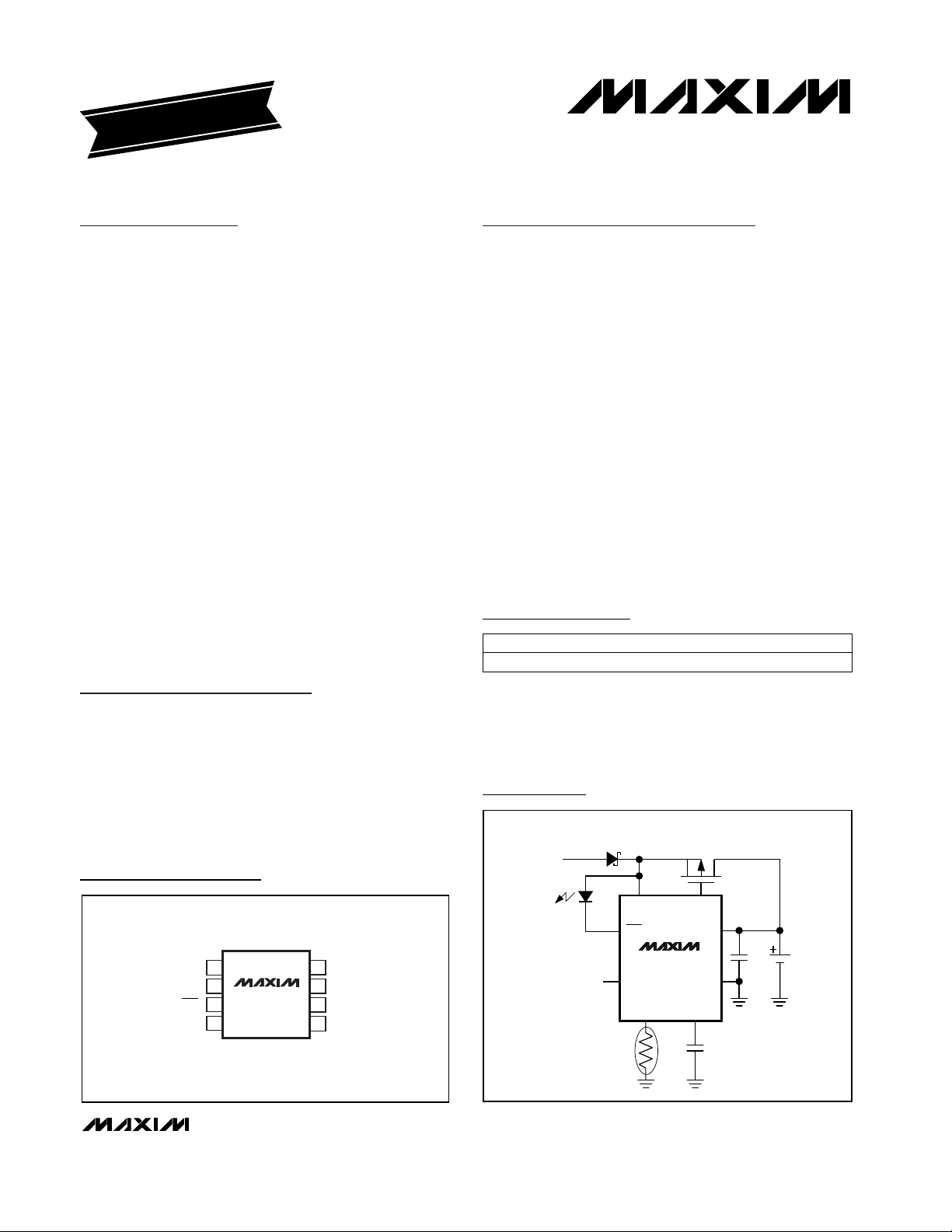
Typical Operating Circuit
19-1545; Rev 0; 9/99
EVALUATION KIT
AVAILABLE
Pin Configuration
Ordering Information
PIN-PACKAGETEMP. RANGEPART
8 µMAX-40°C to +85°CMAX1679EUA
TOP VIEW
GATE
CHG
1
IN
2
MAX1679
3
4
µMAX
8
7
6
5
BATT
THERM
GND
ADJTSEL
CURRENT-
LIMITED
VOLTAGE
SOURCE
LED
TIMER
RANGE
SELECT
THERMISTOR
IN
CHG
TSEL
THERM ADJ
PFET
GATE
BATT
BATTERY
MAX1679
GND
%
MAX1679
Single-Cell Li+ Battery Charger
for Current-Limited Supply
2 _______________________________________________________________________________________
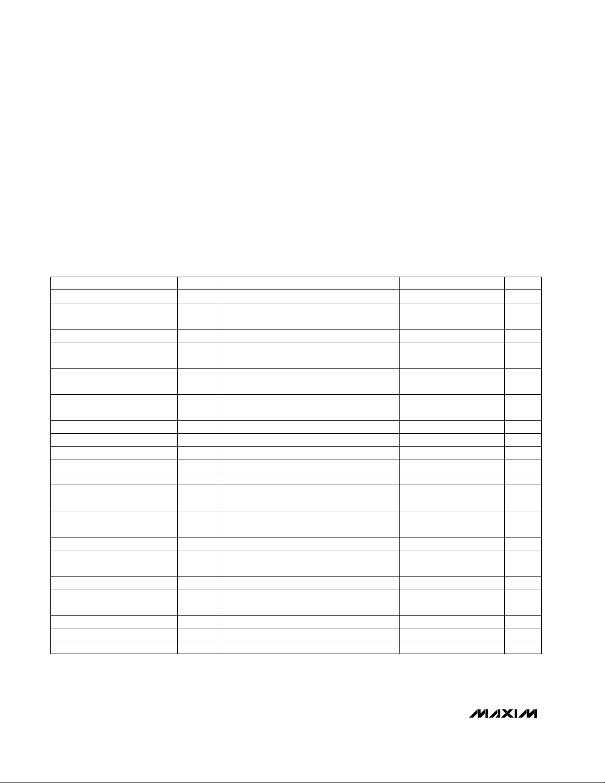
ELECTRICAL CHARACTERISTICS
(VIN= V
CHG
= +10V, V
BATT
= +4.2V, TSEL = GND, GATE = unconnected, ADJ = unconnected, THERM = 10kΩ to GND, TA= 0°C
to +85°C, unless otherwise noted. Typical values are at T
A
= +25°C.)
IN, CHG, GATE to GND ........................................ -0.3V to +26V
BATT, TSEL, THERM, ADJ to GND ........................ -0.3V to +6V
GATE to IN................................................................-6V to +0.3V
THERM, ADJ to BATT...............................................-6V to +0.3V
GATE Continuous Current ................................................ -10mA
Continuous Power Dissipation (T
A
= +70°C)
8-Pin µMAX (derate 4.1mW/°C above +70°C) ........... 330mW
Operating Temperature Range ...........................-40°C to +85°C
Storage Temperature Range ............................ -65°C to +150°C
Lead Temperature (soldering, 10sec) ............................ +300°C
PARAMETER SYMBOL MIN TYP MAX UNITSCONDITIONS
CHG Output Leakage Current
-1 +1 µA
V
CHG
= 22V, CHG = high
Timer Accuracy -10 +10 %See Table 3
IN Input Current, Done State I
IN
250 600 µAV
BATT
= 4.25V, VIN= 22V
IN Input Current, Fast-Charge
State
I
IN
30 100 µAV
BATT
= 4V, VIN= 4V
BATT Input Current, Done State I
BATT
500 1000 µAV
BATT
= 4.25V
BATT Input Current, FastCharge State
I
BATT
900 1500 µAV
BATT
= 4V
BATT Input Current (Note 2) 0.1 1 µAVIN≤ V
BATT
-0.3V
Battery Removal Detection
Threshold
4.875 5.0 5.125 VV
BATT
rising
Battery Removal Detection
Threshold Hysteresis
125 mVV
BATT
falling
BATT Regulation Adjust Range 4.0 4.2 V
Precharge Source Current 456mA
Fast-Charge Restart Threshold 3.783 3.89 4.00 V
Fast-Charge Qualification
Threshold
2.425 2.500 2.575 V
Undervoltage Lockout Trip-Point
Hysteresis
60 mV
BATT Regulation Voltage 4.1685 4.2000 4.2315 V
Input Voltage for Removable
Battery (Note 1)
Input Voltage (Note 1) V
IN
522V
V
IN
622V
Undervoltage Lockout Trip Point 2.1 2.2 2.3 V
V
BATT
= 2V
V
BATT
falling, transition from DONE to
PREQUAL state (Figure 2)
V
BATT
rising, transition from precharge to full
current
V
BATT
falling
External PMOS FET off
External PMOS FET off
V
BATT
rising
ABSOLUTE MAXIMUM RATINGS
Stresses beyond those listed under “Absolute Maximum Ratings” may cause permanent damage to the device. These are stress ratings only, and functional
operation of the device at these or any other conditions beyond those indicated in the operational sections of the specifications is not implied. Exposure to
absolute maximum rating conditions for extended periods may affect device reliability.
ADJ Source Impedance 9.8 10 10.2 kΩ
ADJ Output Voltage 1.393 1.400 1.407 VNo load on ADJ
%
Single-Cell Li+ Battery Charger
for Current-Limited Supply
MAX1679
_______________________________________________________________________________________ 3
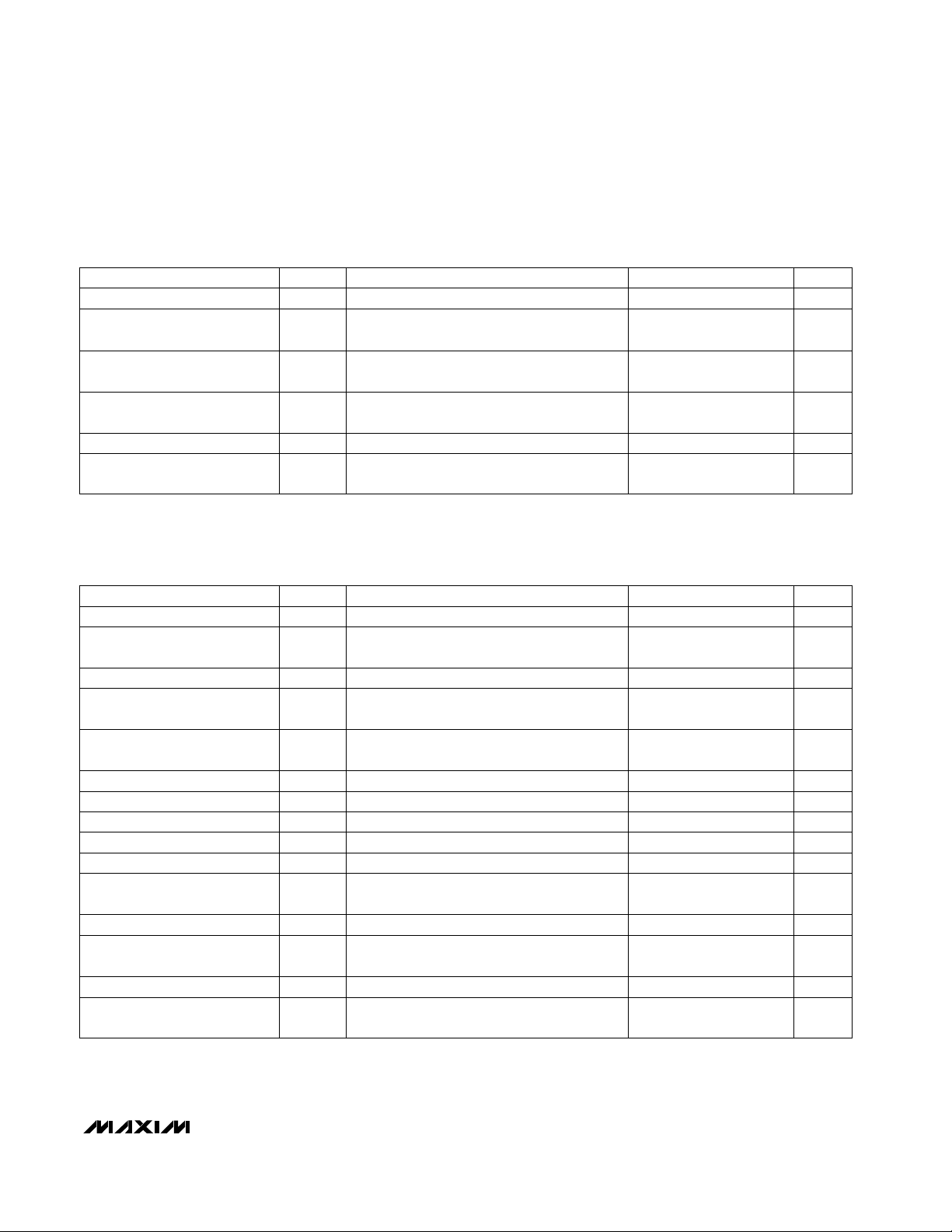
PARAMETER SYMBOL MIN TYP MAX UNITSCONDITIONS
GATE Drive Current at Battery
Removal
20 40 60 mAV
BATT
= 5.1V, gate driven high
GATE Source/Sink Current 75 105 130 µAVIN= 10V, V
GATE
= 8V
THERM Sense Voltage Trip
Point
1.379 1.40 1.421 V
THERM Sense Current (for cold
qualification)
47.8 48.8 49.8 µA
THERM Sense Current (for hot
qualification)
346 352.9 360 µA
CHG Output Sink Current
456mA
V
CHG
= 1V, CHG = low
ELECTRICAL CHARACTERISTICS (continued)
(VIN= V
CHG
= +10V, V
BATT
= +4.2V, TSEL = GND, GATE = unconnected, ADJ = unconnected, THERM = 10kΩ to GND, TA= 0°C
to +85°C, unless otherwise noted. Typical values are at T
A
= +25°C.)
ELECTRICAL CHARACTERISTICS
(VIN= V
CHG
= +10V, V
BATT
= +4.2V, TSEL = GND, GATE = unconnected, ADJ = unconnected, THERM = 10kΩ to GND, TA= -40°C
to +85°C, unless otherwise noted.)
BATT Regulation Adjust Range 4.0 4.2 V
Undervoltage Lockout Trip Point 2.05 2.35 VV
BATT
rising
PARAMETER SYMBOL MIN MAX UNITS
Precharge Source Current 37mA
Fast-Charge Restart Threshold 3.74 4.04 V
Fast-Charge Qualification
Threshold
2.35 2.65 V
BATT Regulation Voltage 4.137 4.263 V
Input Voltage for Removable
Battery (Note 1)
Input Voltage (Note 1) V
IN
522V
V
IN
622V
CONDITIONS
V
BATT
= 2V
V
BATT
falling, transition from DONE to
PREQUAL state, Figure 2
V
BATT
rising, transition from precharge to full
current
ADJ Source Impedance 9.8 10.2 kΩ
External PMOS FET off
External PMOS FET off
ADJ Output Voltage 1.386 1.414 VNo load on ADJ
Battery Removal Detection
Threshold
4.850 5.150 VV
BATT
rising
BATT Input Current (Note 2) 1 µAVIN≤ V
BATT
- 0.3V
BATT Input Current, FastCharge State
I
BATT
1500 µAV
BATT
= 4.0V
BATT Input Current, Done State I
BATT
1000 µAV
BATT
= 4.25V
IN Input Current, Fast-Charge
State
I
IN
100 µAV
BATT
= 4.0V, VIN= 4.0V
MAX1679
Single-Cell Li+ Battery Charger
for Current-Limited Supply
4 _______________________________________________________________________________________
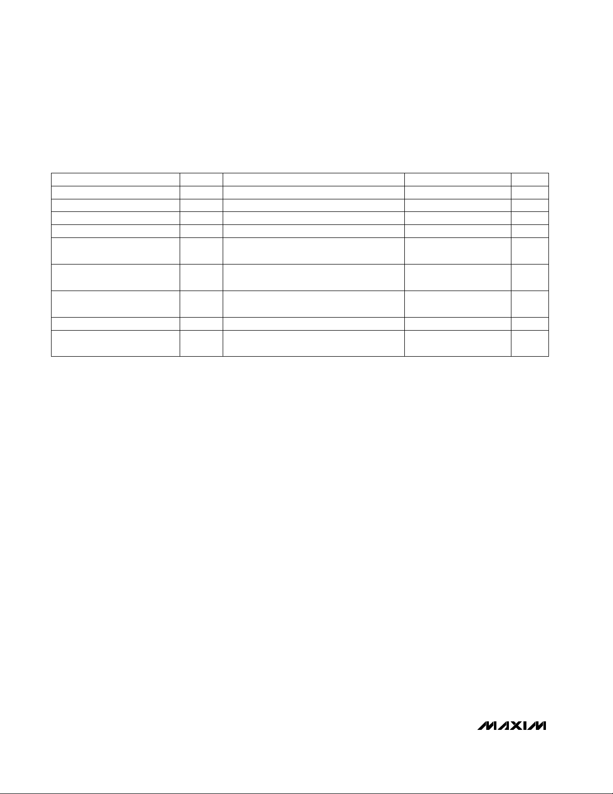
THERM Sense Voltage Trip
Point
1.358 1.442 V
GATE Drive Current at Battery
Removal
20 90 mAV
BATT
= 5.1V, gate driven high
GATE Source/Sink Current 60 140 µAVIN= 10V, V
GATE
= 8V
PARAMETER SYMBOL MIN MAX UNITS
THERM Sense Current (for cold
qualification)
47.3 50.3 µA
THERM Sense Current (for hot
qualification)
342 363 µA
CHG Output Sink Current
46mA
V
CHG
= 1.0V, CHG = low
CHG Output Leakage Current
-1 +1 µA
V
CHG
= 22V, CHG = high
Timer Accuracy -15 +15 %See Table 3
IN Input Current, Done State I
IN
700 µAV
BATT
= 4.25V, VIN= 22V
CONDITIONS
ELECTRICAL CHARACTERISTICS (continued)
(VIN= V
CHG
= +10V, V
BATT
= +4.2V, TSEL = GND, GATE = unconnected, ADJ = unconnected, THERM = 10kΩ to GND, TA= -40°C
to +85°C, unless otherwise noted.)
Note 1: The input voltage range is specified with the external PFET off. When charging, the PFET turns on and the input voltage
(the output voltage of the constant-current power source) drops to very near the battery voltage. When the PFET is on, V
IN
may be as low as 2.5V.
Note 2: BATT Input Current is the supply current to the device. When VINis removed, the MAX1679 shuts down and the input current
is less than 1µA, even if there is an external R
ADJ
resistor (ADJ to GND).

Single-Cell Li+ Battery Charger
for Current-Limited Supply
MAX1679
_______________________________________________________________________________________ 5
Typical Operating Characteristics
(VIN= V
CHG
= +10V, V
BATT
= +4.2V, THERM = 10kΩ to GND, TA= +25°C, unless otherwise noted.)
4.0
4.8
4.4
4.6
4.2
5.2
5.0
5.8
5.6
5.4
6.0
51510 20 25
PRECHARGE CURRENT
vs. INPUT VOLTAGE
MAX1679 toc03
VIN (V)
PRECHARGE CURRENT (mA)
V
BATT
= 4.1V
V
BATT
= 2V
V
BATT
= 0V
0.9975
0.9985
0.9980
0.9995
0.9990
1.0010
1.0005
1.0000
1.0015
-40 0-20 20 40 60 80 100
NORMALIZED BATT REGULATION VOLTAGE
vs. TEMPERATURE
MAX1679 toc02
TEMPERATURE (°C)
BATT REGULATION VOLTAGE
NORMALIZED TO +25°C
Pin Description
Battery Regulation Voltage Adjustment. Bypass to GND with a 1000pF capacitor. Connect a resistor from
ADJ to GND to reduce the nominal +4.200V regulation setpoint. See
Adjusting the Battery Regulation
Voltage
.
ADJ5
Ground. See
Layout Guidelines
for information on system grounding. Connect the battery’s negative termi-
nal to GND.
GND6
Thermistor Temperature-Sensor Input. Connect a thermistor from THERM to GND to prequalify the cell temperature for fast-charge. Drive THERM high (> +1.4V) during Done or Fault states to reset the MAX1679 and
reinitiate the charging sequence. Replace the thermistor with a 10kΩ resistor if temperature sensing is not
required.
THERM7
Cell Voltage Monitor Input, Trickle-Charge Output, and MAX1679 Power Source. Connect BATT to the positive terminal of a single Li+ cell. Bypass BATT with a capacitor to ground (1.5µF per amp of charge current).
BATT8
Maximum Total Charge-Time Selection. See Table 3 for timer options.TSEL4
Charge Status Indication. CHG is an open-drain, current-limited N-channel MOSFET suitable for directly driving an LED. Connect a pull-up resistor to BATT to generate a logic-level signal. See Table 2 for CHG output states.
CHG
3
PIN
Gate Drive for External PMOS Pass Element. The PMOS device should have a VGSthreshold of 2.5V or
less. See
Selecting External Components
.
GATE2
Input Voltage from Current-Limited Voltage Source (+22V max). Bypass to GND with a 0.1µF capacitor. The
cell charging current is set by the current limit of the external power supply.
IN1
FUNCTIONNAME
1.0200
1.0150
1.0100
1.0050
TIMER PERIOD
1.0000
0.9950
0.9900
TIMER PERIOD vs.
AMBIENT TEMPERATURE
NORMALIZED TO +25°C
-40 20 40-20 0 60 80 100
TEMPERATURE (°C)
MAX1679 toc01

6 _______________________________________________________________________________________
MAX1679
Single-Cell Li+ Battery Charger
for Current-Limited Supply
Figure 1. Functional Diagram
CURRENT-LIMITED
VOLTAGE SOURCE
(800mA)
TSEL
SEE TABLE 3
FOR TIMEOUT
OPTIONS
TRICKLE
CHARGE
(5mA)
TIMER
30kHz
OSCILLATOR
REVERSE-CURRENT
PROTECTION DIODE
MAX1679
MACHINE
STATE
HOT
QUAL
TEST
CURRENT
1.4V
BATT REMOVED
COLD
QUAL
TEST
CURRENT
PFET
10kΩ
1.4V
5mA
CHG
BATT
1:3
5V
ADJ
1nF
2.2µF
R
ADJ
**
SINGLE
Li+
CELL
*
IN GATE
THERM
NTC THERMISTOR*
*OPTIONAL
**R
= 410kΩ ±1% FOR 4.1V CELL; LEAVE OPEN FOR 4.2V CELL.
ADJ

MAX1679
Single-Cell Li+ Battery Charger
for Current-Limited Supply
_______________________________________________________________________________________ 7
CELL NOT INSTALLED
Figure 2. State Machine Diagram
(FROM ANY STATE)
PREQUALIFICATION
LED: 50% DUTY CYCLE, 2Hz
PMOS FET: OFF
5mA PRECHARGE: ON
TEMPERATURE NOT OK
OR V
BATT
< 2.5V
CHARGER POWER
APPLIED
TEMPERATURE OK
AND V
BATT
EVERY 7sec
SHUTDOWN
LED: OFF
PMOS FET: OFF
V
PULL THERM HIGH
>
2.5V
FAST-CHARGE
LED: ON
PMOS FET: ON
CHARGING POWER REMOVED
(FROM ANY STATE)
CELL REMOVAL OR
PULL THERM HIGH
BATT
<3.89VOR
FAST-CHARGE
TIMEOUT
FAULT
LED: 50% DUTY CYCLE, 2Hz
PMOS FET: OFF
FAST-CHARGE QUALIFICATION
LED: ON
PMOS FET: OFF
TEMPERATURE NOT OK
TOP-OFF QUALIFICATION
LED: ON
PMOS FET: OFF
TEMPERATURE NOT OK
TEMPERATURE OK
EVERY 7sec
TOP OFF
LED: ON
PMOS FET: PULSED TOP-OFF
TEMPERATURE OK
CELL VOLTAGE REACHES
BATT REGULATION VALUE (e.g., 4.2V)
FET ON TIME
FET OFF TIME
≤ 1%
DONE
LED: 12% DUTY CYCLE, 0.25Hz
PMOS FET: OFF
5mA CANCELLATION CURRENT ENABLED

MAX1679
Detailed Description
Initiating a Charge Cycle
The MAX1679 attempts to initiate fast-charge upon
insertion of the battery or application of an external
power source (current-limited wall cube). After charge
completion, charging restarts when the cell voltage
drops below 3.89V or when THERM is pulled above 1.4V.
Before a charge cycle can begin, the cell conditions
are verified to be within safe limits. The cell voltage
must be greater than 2.5V but less than the regulation
voltage (default value 4.2V). In addition, the thermistor
must indicate an acceptable cell temperature (the
default range is +2.5°C to +47.5°C). See the
Appli-
cations Information
section.
Li+ cells can be damaged when fast-charged from a
completely dead state. Moreover, a fully discharged
cell may indicate a dangerously abnormal cell condition. As a built-in safety feature, the MAX1679
precharges the Li+ cell with 5mA at the start of a
charge cycle when the cell voltage is below 2.5V.
Typically, 5mA is sufficient to bring a fully discharged
1000mAh Li+ cell up to 2.5V in less than 5 minutes. As
soon as the cell’s voltage reaches 2.5V and all the
other prerequisites are met (see the
Fast-Charge
sec-
tion), the MAX1679 begins fast-charging the cell.
If the temperature is outside the programmed range,
the charger waits. Once all prequalification conditions
are met, the charging cycle and timers begin. The
MAX1679 continues to monitor these conditions
throughout the charging cycle.
Fast-Charge
Once all cell conditions are determined to be satisfactory, the MAX1679 begins fast-charging the Li+ cell by
turning on the external PMOS FET. The cell charging
current is set by the current limit of the external
power supply; it is
not
regulated by the MAX1679. The
PMOS FET is used as a simple switch, not as a linear
regulator. Therefore, the circuit’s power dissipation is
minimized, permitting rapid charge cycles with minimal
heat generation. The external power supply should
have a specified current limit that matches the desired
fast-charge current for the Li+ cell.
Fast-charge continues until one of the following conditions is reached: 1) cell voltage climbs to the battery
regulation voltage (4.2V or as set by ADJ); 2) the fastcharging timer expires (fault condition); or 3) cell temperature rises above +47.5°C or falls below +2.5°C. If
the cell temperature moves outside the specified limits,
charging is suspended but not terminated. All timers are
paused and charging resumes when the temperature
returns to the normal range.
Pulsed Top-Off Charge
In the most common case, where fast-charge is terminated because the battery regulation voltage has been
reached (that is, the cell is nearly fully charged), the
MAX1679 will top off the cell. The MAX1679 uses a hysteretic algorithm with minimum on-times and minimum
off-times (Table 3). The cell voltage is sampled every
2ms. If the cell voltage (at BATT) is less than the battery
regulation voltage, the external PMOS FET turns on or
remains on. If the cell voltage is greater than, or equal
to, the battery regulation voltage, the FET turns off or
remains off until the next sample. By also measuring
the cell voltage when the PMOS FET is off, the
MAX1679 eliminates voltage errors caused by charging
current flowing through the series resistance of protection
switches or fuse links that may be in the charging path.
At the beginning of this top-off state, the current stays
on for many consecutive cycles between single off periods. As the cell continues to charge, the percentage of
time spent in the “current-on” mode decreases. Toward
the end of top off, the current stays off for many cycles
between single “on” pulses. During these final pulses,
the instantaneous cell voltage may exceed the battery
regulation voltage by several hundred millivolts, but the
duration of these pulses is several orders of magnitude
shorter than the intrinsic chemical time constant of Li+
cells. This does not harm the cell. Cell top off is completed either when the duty ratio of “on” cycles to “off”
cycles falls below 1/64 to 1/256 as set by TSEL (see
Table 3), or when the charging timer expires.
Switched 5mA Cancellation Current
When the charge cycle is complete, the MAX1679
replaces current drawn by the BATT pin (to sense battery removal) with a 5mA (nominal) switched current.
This current is turned on and off by an on-chip comparator as needed to maintain the battery regulation
voltage. The cell is maintained in this manner as long
as the battery is inserted and power is connected. This
cancellation current is turned off when the MAX1679 is
shut down. Note that BATT draws less than 1µA from
the battery when power is removed.
Charge Status with CHG
CHG indicates the cell’s charging status. An LED can
be connected directly from IN to CHG for a visible indicator. Alternatively, a pull-up resistor (typically 100kΩ)
from a logic supply to CHG provides a logic-level output.
Table 2 relates the status of the CHG to the condition of
the charger.
Single-Cell Li+ Battery Charger
for Current-Limited Supply
8 _______________________________________________________________________________________

Applications Information
The MAX1679 was designed to offer the maximum integration and functionality in the smallest, most basic
application circuit possible. The only necessary external components are a current-limited wall cube, a
PMOS FET, two small capacitors, and a 10kΩ thermis-
tor/resistor. This simple application circuit appears in
Figure 3. Optionally (as shown in Figure 4), an LED can
be added as a charge-state indicator, a resistor (R
ADJ
)
can be used to trim down the maximum charge voltage
from 4.2V, and/or a reverse-current-protection diode
can be added in line at the source.
If the input is shorted, the MAX1679 will not allow current
to flow from BATT back through IN to the source.
However, the body diode inherent in the enhancement-
mode FET would still allow the cell to discharge rapidly.
To prevent this, add a power Schottky diode between
the source and IN as in Figure 4.
Adjusting the Battery Regulation Voltage
A typical Li+ cell should be charged at a constant current until it reaches a voltage of about 4.2V, then
charged at this voltage until the current decays below a
predetermined level. The MAX1679 provides a simple
way to reduce this maximum target voltage with a single resistor between ADJ and GND. Internally, ADJ
connects to a precision 1.4V reference through a 10kΩ
resistor. Leave ADJ open for a battery regulation voltage (VBR) of 4.2V; connect a 1% resistor from ADJ to
GND to form a voltage divider for lower battery regulation voltage (V
BR¢).
Select the external value using:
A 1% tolerance resistor at ADJ degrades system accuracy by only a fraction of a percent. For example, an
R
ADJ
of 410kΩ ±1% reduces the battery regulation volt-
age by 2.4% (V
BR
¢
= 4.1V from equation above, and
(V
BR
¢
- VBR) / VBR= (4.1 - 4.2) / 4.2 = -2.4%). Therefore,
the additional system error is simply the R
ADJ
tolerance
multiplied by the percent change in the battery regulation voltage, or (1%)(2.4%) = 0.024%.
¢
MAX1679
Single-Cell Li+ Battery Charger
for Current-Limited Supply
_______________________________________________________________________________________ 9
CHG
High impedance
No battery or no charger, or
cell voltage < 2.2V
CONDITION
Low (LED on)
Fast-charge or pulsed topoff charge in progress
LED blinking 0.5sec on (low),
3.5sec off (high impedance)
Charge cycle complete
2Hz, 50% duty factor (LED
flashing)
Fast-charge timer expiration
or initial prequalification state
(V
BATT
< 2.5V or initial tem-
perature fault)
Table 2. CHG Output States
Figure 3. Simple Application Circuit
Figure 4. Application Circuit Including LED, Thermistor, and
Reverse-Current Protection Diode
R
ADJ
=
10k
Ω
V
BR
V'
−
1
GATE
MAX1679
THERM
10k
PMOS FET
FAIRCHILD FDC638P
-4.5A, -20V
0.07Ω AT V
CURRENT-LIMITED
WALL CUBE
(800mA, 6V max)
IN
CHG
ADJ
0.001µF
*SEE TABLE 3 FOR TSEL POSITION AND ASSOCIATED TIMER SETTINGS.
BATT
TSEL*
GS
2.2µF
= -2.5V
SINGLE
Li+
CELL
GATE
MAX1679
THERM
NTC THERMISTOR
FENWAL
140-103LAG-RBI
(10kΩ AT 25°C)
PMOSFET
FAIRCHILD FDC638P
-4.5A, -20V
0.07Ω AT V
BATT
TSEL*
2.2µF
= -2.5V
GS
SINGLE
Li+
CELL
CURRENT LIMITED
WALL CUBE
(800mA, 6V max)
0.001µF
*SEE TABLE 3 FOR TSEL POSITION AND ASSOCIATED TIMER SETTINGS.
** R
ADJ
FOR 4.2V.
SCHOTTKY DIODE
30V, 1A
ZETEX ZHCS1000
5mA
LED
R
410k
1%**
SETS BATTERY REGULATION VOLTAGE TO 4.10V; LEAVE OPEN
IN
CHG
ADJ
ADJ

MAX1679
Selecting Maximum Charge Time
As a safety feature, fast-charging and pulsed top-off
charging will stop if their respective counters time out.
The MAX1679 offers a choice of three timeout periods
set by TSEL (Table 3). In Table 3, C represents the nominal capacity of the battery cell in ampere hours.
Both timers begin upon entering the fast-charge state.
The fast-charge timer is disabled upon leaving fastcharge; the total charge timer continues through top-off
but is disabled in the done state.
Selecting External Components
Power Supply
One reason the MAX1679 Li+ cell-charging solution is
so compact and simple is that the charging current is
set by the external power source, not by the MAX1679
charging circuit. The PMOS FET in this application circuit is either on or off, allowing the source to be directly
connected to the cell or completely disconnected.
Therefore, it is very important to choose a power supply
with current limiting. In most applications, this will be a
small “wall cube” switching converter with an output
voltage limit of about 5V or 6V, which is advertised as
“current-limited” or “constant current.”
PMOS Switch
The PMOS FET is used to switch the current-limited
source on and off into the Li+ cell. Because of the intentionally slow switching times and limited slew rate, the
MAX1679 is not particular about the power FET it drives.
Specifications to consider when choosing an appropriate
FET are the minimum drain-source breakdown voltage,
the minimum turn-on threshold voltage (VGS), and current
handling and power-dissipation qualities. The minimum
breakdown voltage (BVDS) must exceed the open-circuit
voltage of the wall cube by at least 25%. Note that this
open-circuit voltage may be twice as high as the specified
output voltage, depending on the converter type.
Thermistor
The intent of THERM is to inhibit fast-charging the cell
when it is too cold or too hot (+2.5°C ≤ TOK≤ 47.5°C),
using an external thermistor. THERM time multiplexes
two sense currents to test for both hot and cold qualification. The thermistor should be 10kΩ at +25°C and
have a negative temperature coefficient (NTC); the
THERM pin expects 3.97kΩ at +47.5°C and 28.7kΩ at
+2.5°C. Connect the thermistor between THERM and
GND. If no temperature qualification is desired, replace
the thermistor with a 10kΩ resistor. Thermistors by
Philips (22322-640-63103), Cornerstone Sensors
(T101D103-CA), and Fenwal Electronics (140-103LAGRB1) work well.
Bypass Capacitors
Bypass the ADJ pin with a 0.001µF ceramic capacitor.
Bypass BATT with a capacitor with a value of at least
1.5µF per amp of charge current. The MAX1679 has a
built-in protection feature that prevents BATT from rising
above 5.5V. The device recognizes a rapid rise at BATT,
indicating that the cell is being removed with the FET
on. A capacitor from BATT to GND that’s too small does
not give the MAX1679 adequate time to shut off the FET.
BATT may then rise above 6V (towards the open-circuit
source voltage), violating the absolute maximum rating
and damaging the device.
In applications where the cell is removable, very large
capacitance values make it increasingly difficult to identify momentary cell removal events and may increase
transient currents when the cell is replaced. Therefore,
values in excess of 100µF should be avoided in those
cases. For best system performance, at least 0.47µF of
the total capacitance should be low-ESR ceramic.
Single-Cell Li+ Battery Charger
for Current-Limited Supply
10 ______________________________________________________________________________________
3.75ADJ
TOTAL
CHARGE
TIME LIMIT
(hours)
2.8
6.25GND
140
BATT
TSEL
CONNECTION
MIN
ON/OFF TIME
(IN TOP-OFF)
(ms)
70
280
75
Off
55
FAST-
CHARGE
TIME LIMIT
(minutes)
Table 3. Timer Option (TSEL) Definitions
1C
<1C
1.5C
RECOMMENDED
CHARGE RATE
1/128
ON/OFF DUTY
CYCLE
FOR DONE
INDICATION
1/256
1/64

Layout Guidelines
The MAX1679 controls the GATE slew rate. The layout is
not as sensitive to noise as a high-frequency switching
regulator. In addition, since the cell voltage is sensed
both during and between high-current pulses, the system is insensitive to ground drops. However, Maxim recommends establishing good grounding areas and large
traces for high-current paths.
Chip Information
TRANSISTOR COUNT: 4692
SUBSTRATE CONNECTED TO GND
MAX1679
Single-Cell Li+ Battery Charger
for Current-Limited Supply
______________________________________________________________________________________ 11

MAX1679
Single-Cell Li+ Battery Charger
for Current-Limited Supply
Maxim cannot assume responsibility for use of any circuitry other than circuitry entirely embodied in a Maxim product. No circuit patent licenses are
implied. Maxim reserves the right to change the circuitry and specifications without notice at any time.
12
____________________Maxim Integrated Products, 120 San Gabriel Drive, Sunnyvale, CA 94086 408-737-7600
© 1999 Maxim Integrated Products Printed USA is a registered trademark of Maxim Integrated Products.
MAX1679
Maxim cannot assume responsibility for use of any circuitry other than circuitry entirely embodied in a Maxim product. No circuit patent licenses are
implied. Maxim reserves the right to change the circuitry and specifications without notice at any time.
12
____________________Maxim Integrated Products, 120 San Gabriel Drive, Sunnyvale, CA 94086 408-737-7600
© 1999 Maxim Integrated Products Printed USA is a registered trademark of Maxim Integrated Products.
Package Information
Note: The MAX1679 does not have an exposed pad.
8LUMAXD.EPS
 Loading...