General Description
The MAX1677 is a compact, high-efficiency, dual-output boost converter for portable devices needing two
regulated supplies, typically for logic and liquid crystal
displays (LCDs). Operation with inputs as low as 0.7V
allows the MAX1677 to accept 1, 2, or 3-cell alkaline,
NiCd, or NiMH batteries as well as 1-cell lithium-ion batteries. The device requires no external FETs and can
maintain regulation while consuming only 20µA, making
it ideal for hand-held pen-input and PDA devices operating with low-current “sleep” states.
The MAX1677’s primary regulator supplies up to
350mA at either a factory-preset 3.3V or an adjustable
2.5V to 5.5V output. On-chip synchronous rectification
provides efficiencies up to 95%. 300kHz (or externally
clocked) pulse-width-modulation (PWM) operation is
particularly suitable for applications needing low noise,
such as those with wireless features. The primary converter also features pin-selectable pulse-frequencymodulation (PFM) operation that consumes only 20µA.
A 1µA shutdown state also minimizes battery drain.
The MAX1677’s secondary step-up converter supplies up
to +28V or -28V for LCD bias, varactor tuning, or other
high-voltage, low-current functions. Other MAX1677 features include precision reference, logic control inputs for
both regulators, and an uncommitted comparator for
low-battery detection or a reset function. The MAX1677
is supplied in Maxim’s compact 16-pin QSOP package,
which occupies no more space than a standard SO-8.
Applications
PDAs Portable Phones
Hand-Held Terminals Portable Instruments
Features
♦ No External FETs Required
♦ Main Output
Up to 350mA for Logic Supply
Fixed 3.3V or Adjustable (2.5V to 5.5V)
Synchronous Rectification for High Efficiency
(up to 95%)
300kHz (200kHz to 400kHz Synchronizable)
Fixed-Frequency PWM Operation
♦ Secondary Output
Up to +28V or -28V for LCD Bias
Programmable Current Limit
♦ 0.7V to 5.5V Input Voltage Range
♦ 20µA Quiescent Current
♦ 1µA Shutdown Current
♦ Low-Battery Comparator
♦ Small 16-Pin QSOP Package
MAX1677
Compact, High-Efficiency, Dual-Output
Step-Up and LCD Bias DC-DC Converter
________________________________________________________________
Maxim Integrated Products
1
16
15
14
13
12
11
10
9
1
2
3
4
5
6
7
8
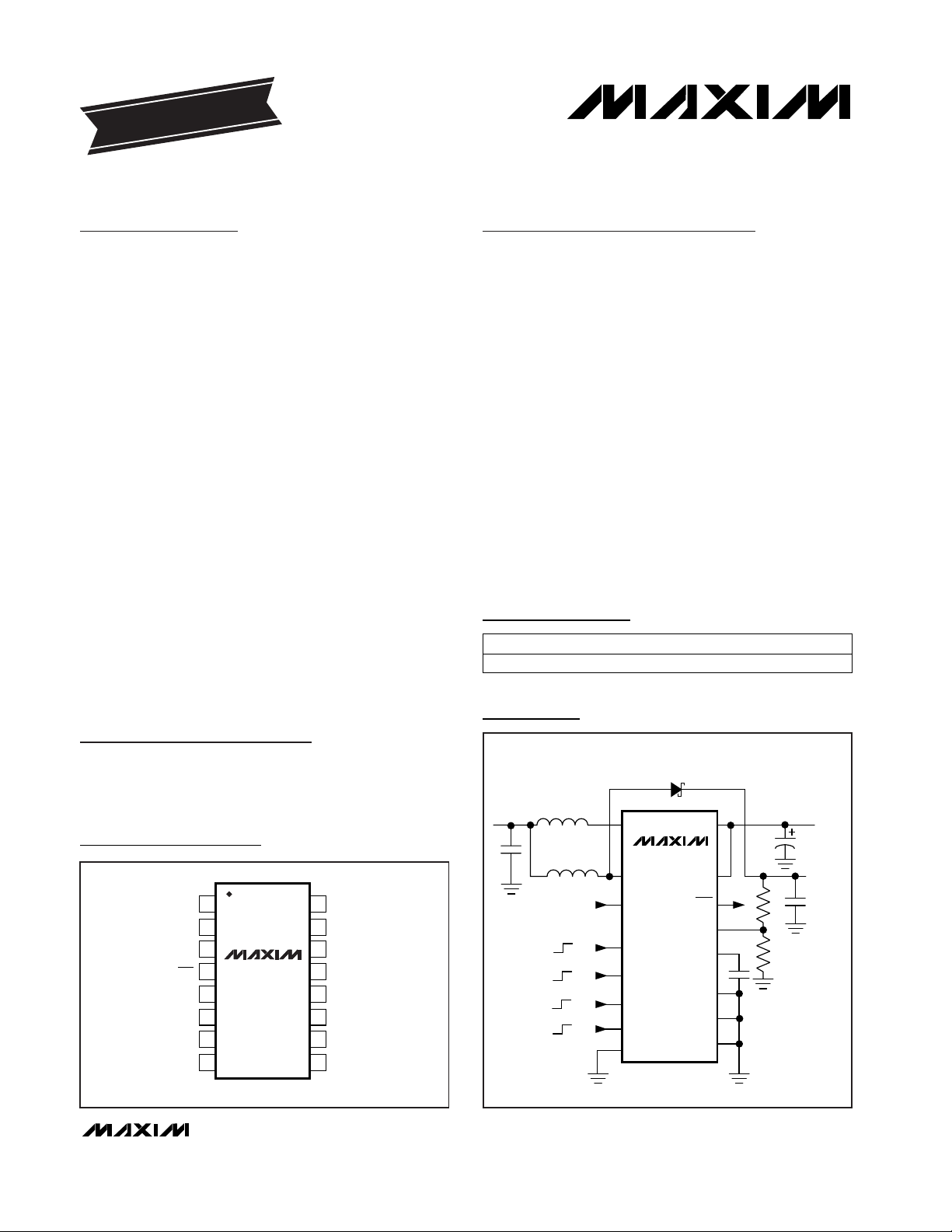
OUT POUT
LX
PGND
LCDGND
LCDLX
ON
LCDFB
GND
TOP VIEW
MAX1677
FB
LBI
LCDON
LBO
CLK/SEL
LCDPOL
REF
QSOP
19-1403; Rev 0; 11/98
PART
MAX1677EEE -40°C to +85°C
TEMP. RANGE PIN-PACKAGE
16 QSOP
EVALUATION KIT MANUAL
FOLLOWS DATA SHEET
Pin Configuration
Ordering Information
For free samples & the latest literature: http://www.maxim-ic.com, or phone 1-800-998-8800.
For small orders, phone 1-800-835-8769.
Typical Operating Circuit
MAX1677
LX
POUT
OUT
±28V
LCD
BOOST
OUTPUT
3.3V MAIN
BOOST OUTPUT
LCDFB
REF
FB
LCDGND
GND
LCDLX
LCDON
LBI
ON
OFF
LBO
CLK/SEL
ON
LCDPOL
PGND
PWM
PFM
ON
OFF
+VE OUT
-VE OUT
V
IN
= 0.7V to 5.5V
(UP TO MAIN
OUT
)
MAX1677
Compact, High-Efficiency, Dual-Output
Step-Up and LCD Bias DC-DC Converter
2 _______________________________________________________________________________________
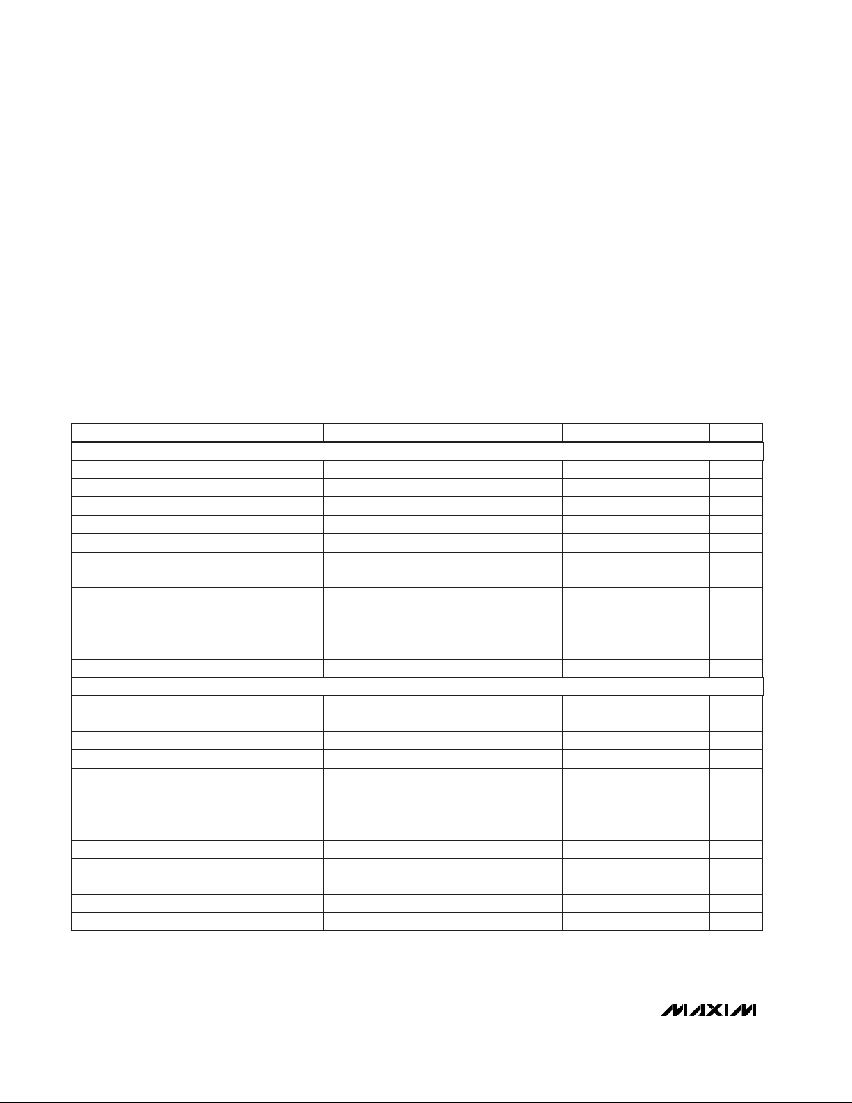
ABSOLUTE MAXIMUM RATINGS
ELECTRICAL CHARACTERISTICS
(V
OUT
= 3.3V, C
REF
= 0.1µF, POUT = OUT, TA= 0°C to +85°C, unless otherwise noted. Typical values are at TA= +25°C.)
Stresses beyond those listed under "Absolute Maximum Ratings" may cause permanent damage to the device. These are stress ratings only, and functional
operation of the device at these or any other conditions beyond those indicated in the operational sections of the specifications is not implied. Exposure to
absolute maximum rating conditions for extended periods may affect device reliability.
OUT, LCDON, ON, POUT, LBI, LBO,
LX to GND .............................................................-0.3V to +6V
CLK/SEL, LCDPOL, REF, LCDFB,
FB to GND.............................................-0.3V to (V
OUT
+ 0.3V)
LCDLX to GND.......................................................-0.3V to +30V
PGND, LCDGND to GND......................................-0.3V to +0.3V
POUT to OUT.........................................................-0.3V to +0.3V
Continuous Power Dissipation (T
A
= +70°C)
16-Pin QSOP (derate 8.3mW/°C above +70°C)...........696mW
Operating Temperature Range ...........................-40°C to +85°C
Junction Temperature......................................................+150°C
Storage Temperature Range.............................-65°C to +160°C
Lead Temperature (soldering, 10sec).............................+300°C
TA= +25°C, I
LOAD
< 1mA
No load, current into OUT
No load, current into OUT
I
REF
= 0
I
REF
= 0 to 50µA (Note 2)
V
OUT
= 2.5V to 5.5V
No load, current into OUT
V0.9 1.1V
STARTUP
Minimum Start-Up Voltage
µA0.3 5Supply Current in Shutdown
µA115 300I
PWM
Supply Current All On,
Main DC-DC in PWM Mode
µA35 60I
PFM
Supply Current All On,
Main DC-DC in PFM Mode
V1.23 1.25 1.27V
REF
Reference Voltage
mV2 15Reference Load Regulation
mV0.2 5Reference Line Rejection
µA20 40I
LCDOFF
Supply Current
Main DC On, LCD Off
MAIN BOOST DC-DC
Output Voltage V
OUT
FB = GND, 0 ≤ ILX≤ 350mA,
CLK/SEL = OUT (Note 3)
3.20 3.30 3.43 V
FB Regulation Voltage V
FB(REG)
Adjustable mode, CLK/SEL = OUT (Note 3) 1.225 1.25 1.275 V
FB Input Current I
FB
VFB= 1.3V 0.02 50 nA
Output Voltage Adjustment
Range
2.5 5.5 V
Start-Up to Normal Mode
Transition Voltage (Note 4)
V
LOCKOUT
2.1 2.4 V
Line Regulation I
OUT
= 150mA, VIN= 2V to 3V 0.6 %
Load Regulation
CLK/SEL = OUT, VIN= 2.4V,
I
LOAD
= 10mA to 200mA
1 %
Frequency in Start-Up Mode f
STARTUPVOUT
= 1.5V 40 300 kHz
CONDITIONS UNITSMIN TYP MAXSYMBOLPARAMETER
LX Leakage Current I
LX(LEAK)
0.2 5 µA
(Note 1) V0.7 5.5V
IN
Input Voltage Range
GENERAL
MAIN BOOST DC-DC
MAX1677
Compact, High-Efficiency, Dual-Output
Step-Up and LCD Bias DC-DC Converter
_______________________________________________________________________________________ 3
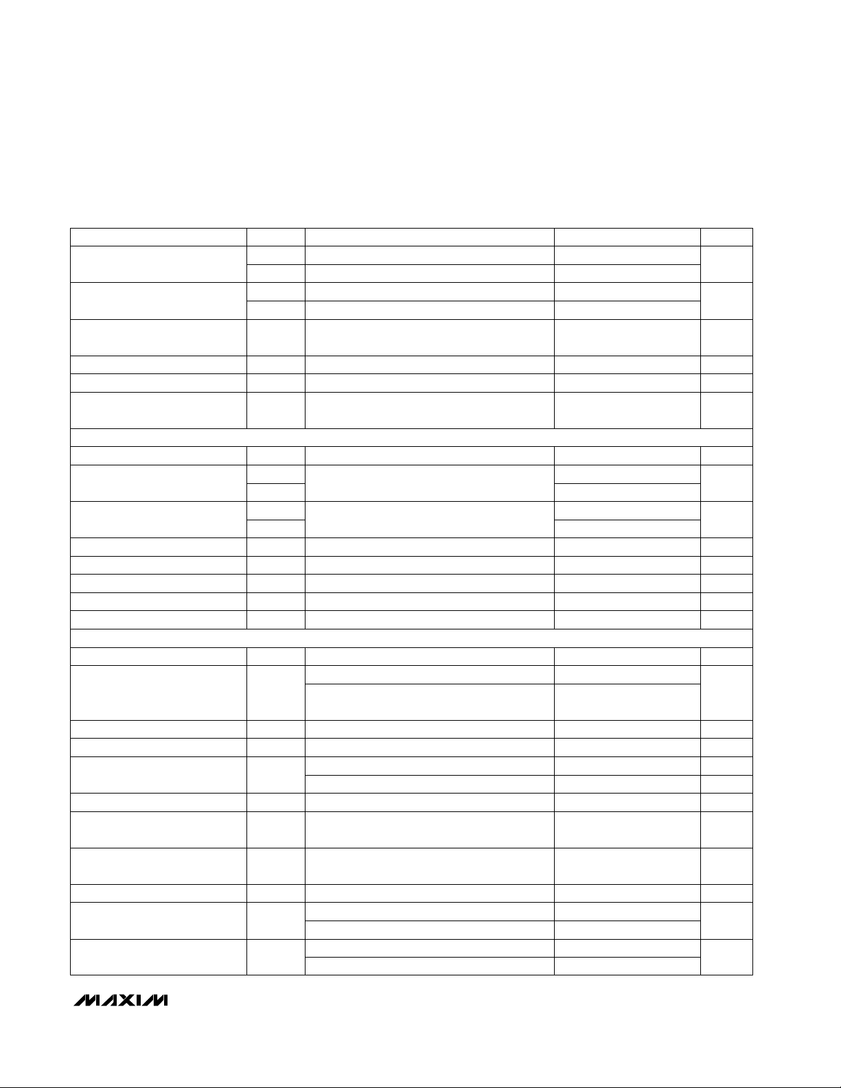
CONDITIONS
N-channel 0.22 0.5
Ω
P-channel 0.4 1.0
LX Current Limit
I
LX(PWM)
N-channel PWM mode 550 670 800
mA
UNITSMIN TYP MAXPARAMETER
I
LX(PFM)
N-channel PFM mode 250 350 450
P-Channel Synchronous Rectifier
Turn-Off Current in PFM Mode
40 90 140 mA
Internal Oscillator f CLK/SEL = OUT 240 300 360 kHz
Oscillator Maximum Duty Cycle D 80 85 90 %
External Clock Frequency
Range
200 400 kHz
LOGIC AND CONTROL
ON Input Threshold
V
ON(LOW)
V
ON(HIGH)
LCDON, LCDPOL, CLK/SEL
Input Threshold
V
IL
V
OUT
> 2.5V
0.2V
OUT
V
V
IH
0.8V
OUT
LBI Falling Threshold V
LBI(TH)
599 614 629 mV
LBI Hysteresis 1 %
LBO Output Low Voltage
V
LBO(LO)
Sink current = 1mA 0.1 V
LBI Input Bias Current I
LBI(BIAS)
50 nA
LBO Leakage Current
I
LBO(LEAK)VLBO
= 5.5V 1 µA
LCDLX Voltage 28 V
LCDPOL connected to OUT or GND through
50kΩ
150 225 300
mA
LCDLX Switch Resistance RLCDLX V
OUT
= 3.3V 1.0 1.4 Ω
LCDLX Leakage Current V
LCDLX
= 28V 1 µA
LCDFB Set Point
Positive LCD, LCDPOL = OUT 1.225 1.25 1.275 V
Negative LCD, LCDPOL = GND -15 0 15 mV
LCDFB Input Bias Current 50 nA
LCD Line Regulation
I
LOAD
= 5mA, VIN= 1.2V to 3.6V,
Figure 2
0.1 %/V
LCD Load Regulation
I
LOAD
= 0 to 5mA, VIN= 2.4V,
Figure 2
0.5 %
Maximum LCDLX On-Time t
ON LCD
3.4 4.3 5.2 µs
1.1V < V
OUT
< 5.5V
0.8V
OUT
0.2V
OUT
V
ELECTRICAL CHARACTERISTICS (continued)
(V
OUT
= 3.3V, C
REF
= 0.1µF, POUT = OUT, TA= 0°C to +85°C, unless otherwise noted. Typical values are at TA= +25°C.)
LX On-Resistance
SYMBOL
R
LX(ON)N
R
LX(ON)P
LCDPOL = OUT or GND 300 350 450
LCDLX Switch Current Limit
Input Leakage Current ON, LCDON, LCDPOL, CLK/SEL 1 µA
Minimum LCDLX Off-Time
Operating mode 0.8 1 1.2
µs
Start-up mode (positive or negative) 3.0 4.0 5.0
LCDFB Voltage for
Start-Up Mode
LCDPOL = OUT 0.75
V
LCDPOL = GND 0.5
LOGIC AND CONTROL INPUTS
LCD BIAS DC-DC
MAX1677
Compact, High-Efficiency, Dual-Output
Step-Up and LCD Bias DC-DC Converter
4 _______________________________________________________________________________________
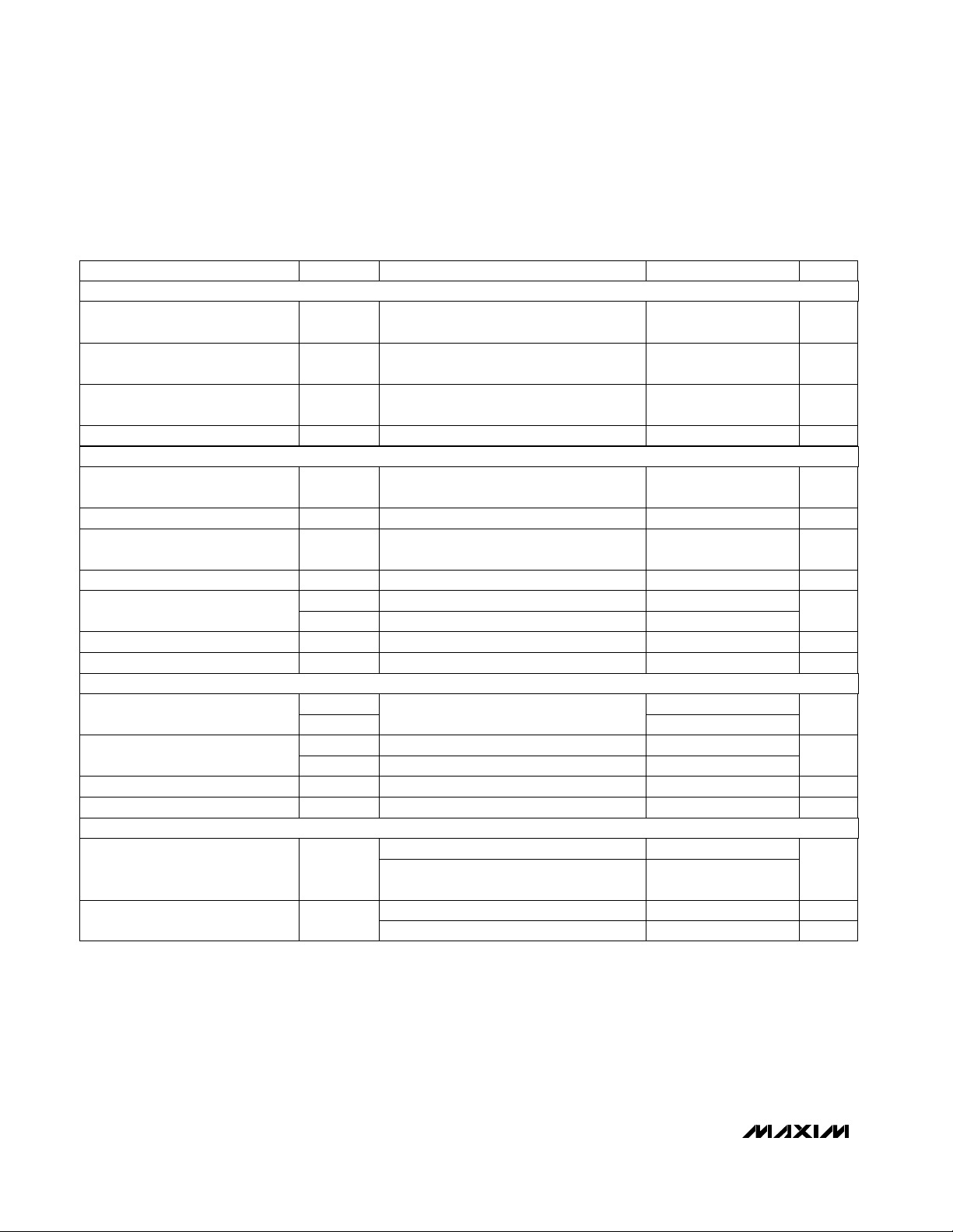
Note 1: The MAX1677 operates in bootstrap mode (operates from the output voltage). Once started, it will operate down to 0.7V
input. If V
IN
exceeds the set V
OUT
, V
OUT
will follow one diode drop below VIN.
Note 2: C
REF
= 0.22µF for applications where I
REF
> 10µA.
Note 3: In low-power mode (CLK/SEL = GND), the output voltage regulates 1% higher than in low-noise mode (CLK/SEL = OUT or
synchronized).
Note 4: The device is in a start-up mode when V
OUT
is below this value.
Note 5: Specifications to -40°C are guaranteed by design and not production tested.
LBO Output Low Voltage
V
LBO(LO)
Sink current = 1mA
LCDPOL = OUT or GND 300 450
0.1 V
µA
Supply Current
Main DC On, LCD Off
Main
Supply Current All On,
Main DC-DC in PFM Mode
I
PFM
No load, current into OUT 60 µA
VFB Regulation Voltage
µALX Leakage Current
Start-Up to Normal Mode Transition
Voltage (Note 4)
CONDITIONS
V
LOCKOUT
2.1 2.4 V
I
LX(LEAK)
5
Output Voltage V
OUT
FB = GND, 0 ≤ ILX≤ 350mA,
CLK/SEL = OUT (Note 3)
3.17 3.4 V
V
FB(REG)
Adjustable mode, CLK/SEL = OUT (Note 3) 1.22 1.28
µA
Supply Current All On,
Main DC-DC in PWM Mode
Supply Current in Shutdown 5 µA
I
PWM
No load, current into OUT 300
General
I
LCDOFF
No load, current into OUT 40
LX Current Limit
I
LX(PWM)
N-channel PWM mode 550 900
mA
UNITSMIN MAXSYMBOLPARAMETER
I
LX(PFM)
N-channel PFM mode 250 500
Internal Oscillator f CLK/SEL = OUT 240 360 kHz
External Clock Frequency Range 200 400 kHz
LOGIC
ON Input Threshold
V
ON(LOW)
1.1V < V
OUT
< 5.5V
0.2V
OUT
V
V
ON(HIGH)
0.8V
OUT
LCDON, LCDPOL, CLK/SEL
Input Threshold
V
IL
0.2V
OUT
V
V
IH
0.8V
OUT
LBI Falling Threshold V
LBI(TH)
599 629 mV
LCD BIAS DC-DC
LCDLX Switch Current Limit
LCDPOL connected to OUT or GND
through 50kΩ
150 300
mA
ELECTRICAL CHARACTERISTICS
(V
OUT
= 3.3V, C
REF
= 0.1µF, POUT = OUT, TA= -40°C to +85°C, unless otherwise noted. ) (Note 5)
LCDFB Set Point
Positive LCD, LCDPOL = OUT 1.22 1.28 V
-20 +20Negative LCD, LCDPOL = GND
GENERAL
MAIN BOOST DC-DC
LOGIC AND CONTROL INPUTS
LCD BIAS DC-DC
mV
MAX1677
Compact, High-Efficiency, Dual-Output
Step-Up and LCD Bias DC-DC Converter
_______________________________________________________________________________________
5
0.1 101 100 1000
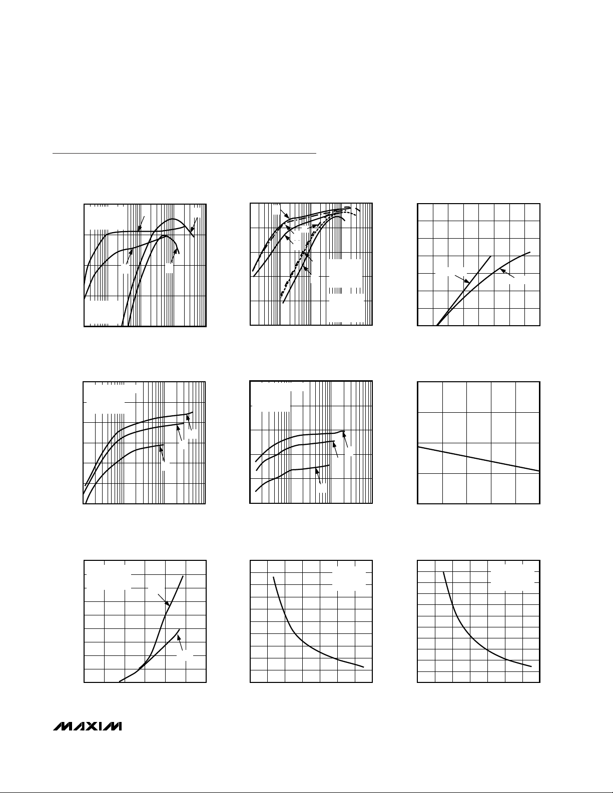
EFFICIENCY vs. LOAD CURRENT
(V
OUT
= 3.3V)
MAX1677-01
LOAD CURRENT (mA)
EFFICIENCY (%)
100
60
70
80
90
PWM MODE
C = 2.4V
D = 1.2V
PFM MODE
A = VIN = 2.4V
B = VIN = 1.2V
C
D
B
A
100
80
60
40
20
0
0.1 1 10 100 1000
EFFICIENCY vs. LOAD CURRENT
(V
OUT
= 5V)
MAX1677-02
LOAD CURRENT (mA)
EFFICIENCY (%)
PWM MODE
A: VIN = 3.6V
B: VIN = 2.4V
C: VIN = 1.2V
A
D
E
F
B
C
PFM MODE
D: VIN = 3.6V
E: VIN = 2.4V
F: VIN = 1.2V
0
100
300
200
500
600
400
700
0 1.0 1.50.5 2.0 2.5 3.0 3.5 4.0
MAXIMUM LOAD CURRENT
vs. BATTERY INPUT VOLTAGE
(PWM MODE)
MAX1677-03
INPUT VOLTAGE (V)
LOAD CURENT (mA)
V
OUT
= 3.3V
V
OUT
= 5V
40
0.1 100101
EFFICIENCY vs. LOAD CURRENT
(LCD V
OUT
= 12V)
100
60
50
80
90
70
MAX1677-04
LOAD CURRENT (mA)
EFFICIENCY (%)
CIRCUIT OF FIGURE 2
A: VIN = 3.6V
B: VIN = 2.4V
C: VIN = 1.2V
A
B
C
50
0.1 100101
EFFICIENCY vs. LOAD CURRENT
(LCD V
OUT
= 20V)
100
70
60
90
80
MAX1677-05
LOAD CURRENT (mA)
EFFICIENCY (%)
CIRCUIT OF FIGURE 2
A: VIN = 3.6V
B: VIN = 2.4V
C: VIN = 1.2V
A
B
C
1.2450
1.2475
1.2525
1.2500
1.2550
0 20 40 60 80 100
REFERENCE VOLTAGE
vs. REFERENCE CURRENT
MAX1677-06
REFERENCE CURRENT (µA)
REFERENCE VOLTAGE (V)
Typical Operating Characteristics
(Circuits of Figures 2 and 3, TA = +25°C, unless otherwise noted.)
0
100
50
250
200
150
400
350
300
450
0 1.00.5 1.5 2.0 2.5 3.0
LOAD CURRENT
vs. START-UP VOLTAGE
MAX1677-07
START-UP VOLTAGE (V)
LOAD CURRENT (mA)
PWM
PFM
V
OUT
= 3.3V
TESTED WITH
RESISTIVE LOAD
0
0.06
0.04
0.02
0.10
0.08
0.18
0.16
0.14
0.12
0.20
0 0.5 1.0 1.5 2.0 2.5 3.0 3.5
NO-LOAD SUPPLY CURRENT vs.
INPUT VOLTAGE (LCD OFF)
MAX1677-08
INPUT VOTAGE (V)
SUPPLY CURRENT (mA)
V
OUT
= 3.3V
PFM MODE
LCD OFF
0
0.1
0.2
0.3
0.4
0.5
0.6
0.7
0.8
0.9
1.0
1.1
0 0.5 1.0 1.5 2.0 2.5 3.0 3.5
NO-LOAD SUPPLY CURRENT vs.
INPUT VOLTAGE (LCD ON)
MAX1677-09
INPUT VOLTAGE (V)
SUPPLY CURRENT (mA)
V
OUT
= 3.3V
PFM MODE
V
LCD
= -20V
 Loading...