

For free samples & the latest literature: http://www.maxim-ic.com, or phone 1-800-998-8800.
For small orders, phone 408-737-7600 ext. 3468.
General Description
The MAX1674/MAX1675/MAX1676 compact, high-efficiency, step-up DC-DC converters fit in small µMAX
packages. They feature a built-in synchronous rectifier,
which improves efficiency and reduces size and cost
by eliminating the need for an external Schottky diode.
Quiescent supply current is only 16µA.
The input voltage ranges from 0.7V to V
OUT
, where
V
OUT
can be set from 2V to 5.5V. Start-up is guaranteed from 1.1V inputs. The MAX1674/MAX1675/
MAX1676 have a preset, pin-selectable output for 5V or
3.3V. The outputs can also be adjusted to other voltages using two external resistors.
All three devices have a 0.3Ω N-channel MOSFET
power switch. The MAX1674 has a 1A current limit. The
MAX1675 has a 0.5A current limit, which permits the
use of a smaller inductor. The MAX1676 comes in a
10-pin µMAX package and features an adjustable current limit and circuitry to reduce inductor ringing.
________________________Applications
Pagers
Wireless Phones
Medical Devices
Hand-Held Computers
PDAs
RF Tags
1 to 3-Cell Hand-Held Devices
____________________________Features
♦ 94% Efficient at 200mA Output Current
♦ 16µA Quiescent Supply Current
♦ Internal Synchronous Rectifier (no external diode)
♦ 0.1µA Logic-Controlled Shutdown
♦ LBI/LBO Low-Battery Detector
♦ Selectable Current Limit for Reduced Ripple
♦ Low-Noise, Anti-Ringing Feature (MAX1676)
♦ 8-Pin and 10-Pin µMAX Packages
♦ Preassembled Evaluation Kit (MAX1676EVKIT)
MAX1674/MAX1675/MAX1676
High-Efficiency, Low-Supply-Current,
Compact, Step-Up DC-DC Converters
________________________________________________________________
Maxim Integrated Products
1
GNDLBO
SHDN
REF
1
2
8
7
OUT
LXLBI
FB
MAX1674
MAX1675
µMAX
TOP VIEW
3
4
6
5
1
2
3
4
5
10
9
8
7
6
OUT
LX
GND
BATTCLSEL
LBO
LBI
FB
MAX1676
µMAX
SHDNREF
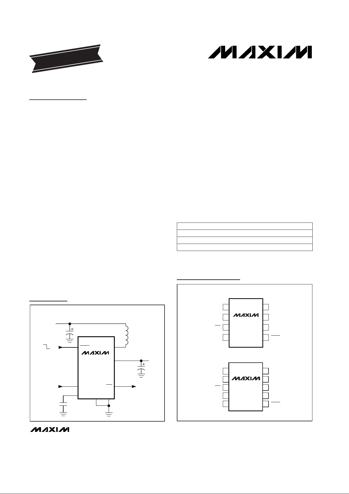
MAX1674
MAX1675
INPUT
0.7V TO V
OUT
SHDN
LX
LBO
OUT
LBI
0.1µF
LOW-BATTERY
DETECT OUT
OFF
ON
REF
GND
FB
OUTPUT
3.3V, 5V, OR
ADJ (2V TO 5.5V)
UP TO 300mA
LOW-BATTERY
DETECT IN
PART
MAX1674EUA
-40°C to +85°C
TEMP. RANGE PIN-PACKAGE
8 µMAX
_______________Ordering Information
MAX1675EUA
-40°C to +85°C 8 µMAX
MAX1676EUB
-40°C to +85°C 10 µMAX
EVALUATION KIT
AVAILABLE
Typical Operating Circuit
Pin Configurations
19-1360; Rev 0; 7/98
MAX1674/MAX1675/MAX1676
High-Efficiency, Low-Supply-Current,
Compact, Step-Up DC-DC Converters
2 _______________________________________________________________________________________
ABSOLUTE MAXIMUM RATINGS
ELECTRICAL CHARACTERISTICS
(V
BATT
= 2V, FB = OUT (V
OUT
= 3.3V), RL= ˙∞, TA= 0°C to +85°C, unless otherwise noted. Typical values are at TA= +25°C.)
Stresses beyond those listed under “Absolute Maximum Ratings” may cause permanent damage to the device. These are stress ratings only, and functional
operation of the device at these or any other conditions beyond those indicated in the operational sections of the specifications is not implied. Exposure to
absolute maximum rating conditions for extended periods may affect device reliability.
Supply Voltage (OUT to GND) ..............................-0.3V to +6.0V
Switch Voltage (LX to GND).....................-0.3V to (V
OUT
+ 0.3V)
Battery Voltage (BATT to GND).............................-0.3V to +6.0V
SHDN, LBO to GND ..............................................-0.3V to +6.0V
LBI, REF, FB, CLSEL to GND...................-0.3V to (V
OUT
+ 0.3V)
Switch Current (LX)...............................................-1.5A to +1.5A
Output Current (OUT) ...........................................-1.5A to +1.5A
Continuous Power Dissipation (T
A
= +70°C)
8-Pin µMAX (derate 4.1mW/°C above +70°C) .............330mW
10-Pin µMAX (derate 5.6mW/°C above +70°C) ...........444mW
Operating Temperature Range ...........................-40°C to +85°C
Junction Temperature......................................................+150°C
Storage Temperature Range.............................-65°C to +165°C
Lead Temperature (soldering, 10sec).............................+300°C
TA= +25°C, RL= 3kΩ (Note 1)
VLX= 0, 5.5V; V
OUT
= 5.5V
TA= +25°C
MAX1675, MAX1676 (CLSEL = GND)
MAX1674, MAX1676 (CLSEL = OUT)
ILX= 100mA
FB = OUT
(V
OUT
= 3.3V)
V
OUT
= 2V to 5.5V
I
REF
= 0 to 100µA
90 130
MAX1675,
MAX1676 (CLSEL = GND)
FB = OUT
FB = GND
I
REF
= 0
CONDITIONS
µA
0.05 1
I
LEAK
LX Leakage Current
A
0.4 0.5 0.65
I
LIM
0.80 1 1.20
LX Switch Current
Limit (NFET)
Ω
0.3 0.6
R
DS(ON)
Internal NFET, PFET
On-Resistance
V
1.274 1.30 1.326
FB, LBI Input Threshold
mV/V
0.08 2.5
V
REF_LINE
Reference Voltage Line
Regulation
mV
3 15
V
REF_LOAD
Reference Voltage Load
Regulation
mV/°C
0.024
TEMPCOReference Voltage Tempco
V
1.274 1.30 1.326
V
REF
Reference Voltage
V
0.9 1.1
Start-Up Voltage
V
1.1 5.5
V
IN
V
0.7
Minimum Input Voltage
Operating Voltage
150 220
FB = GND
(V
OUT
= 5V)
MAX1675,
MAX1676 (CLSEL = GND)
180 285
I
OUT
MAX1674,
MAX1676 (CLSEL = OUT)
mA
300 420
Steady-State Output Current
(Note 2)
mV/°C
-2
Start-Up Voltage Tempco
V
3.17 3.30 3.43
V
OUT
Output Voltage
4.80 5 5.20
MAX1674,
MAX1676 (CLSEL = OUT)
V
2 5.5
Output Voltage Range
UNITSMIN TYP MAXSYMBOLPARAMETER
MAX1674/MAX1675/MAX1676
High-Efficiency, Low-Supply-Current,
Compact, Step-Up DC-DC Converters
_______________________________________________________________________________________ 3
ELECTRICAL CHARACTERISTICS
(V
BATT
= 2V, FB = OUT, RL= ∞, TA= -40°C to +85°C, unless otherwise noted.) (Note 4)
Note 1: Start-up voltage operation is guaranteed with the addition of a Schottky MBR0520 external diode between the input and
output.
Note 2: Steady-state output current indicates that the device maintains output voltage regulation under load. See Figures 5 and 6.
Note 3: Device is bootstrapped (power to the IC comes from OUT). This correlates directly with the actual battery supply.
V
OUT
= 2V, I
LOAD
= 1mA
V
OUT
= 3.3V, I
LOAD
= 200mA
SHDN = GND
CONDITIONS
%
85
Efficiency
90
µA
0.1 1
Shutdown Current into OUT
UNITSMIN TYP MAXSYMBOLPARAMETER
MAX1676, V
BATT
= 2V
V
LBO
= 5.5V, V
LBI
= 5.5V
V
LBI
= 0, I
SINK
= 1mA
V
SHDN
= 0 or V
OUT
VFB= 1V, V
OUT
= 3.3V
MAX1676, CLSEL = OUT
V
LBI
= 1.4V
VFB= 1.4V
VFB= 1V, V
OUT
= 3.3V
0.8V
OUT
V
IH
0.2V
OUT
V
IL
CLSEL Input Voltage
V
0.8V
OUT
V
IH
0.2V
OUT
V
IL
SHDN Input Voltage
Ω88 150Damping Switch Resistance
µA
0.07 1
I
LBO
LBO Off Leakage Current
V
0.2 0.4
LBO Low Output Voltage
nA
0.07 50
I
SHDN
SHDN Input Current
µA
1.4 3
I
CLSEL
CLSEL Input Current
nA
1 50
I
LBI
LBI Input Current
nA
0.03 50
I
FB
FB Input Current
µs
0.8 1 1.2
t
OFF
LX Switch Off-Time
µs
3 4 7
t
ON
LX Switch On-Time
V
ELECTRICAL CHARACTERISTICS (continued)
(V
BATT
= 2V, FB = OUT (V
OUT
= 3.3V), RL= ˙∞, TA= 0°C to +85°C, unless otherwise noted. Typical values are at TA= +25°C.)
FB = GND
FB = OUT
VFB= 1V, V
OUT
= 3.3V
VFB= 1V, V
OUT
= 3.3V
SHDN = GND
VFB= 1.4V, V
OUT
= 3.3V
I
REF
= 0
MAX1675, MAX1676 (CLSEL = GND)
MAX1674, MAX1676 (CLSEL = OUT)
CONDITIONS
0.36 0.69
A
0.75 1.25
I
LIM
LX Switch Current
Limit (NFET)
V2.20 5.5Output Voltage Range
V
4.75 5.25
3.13 3.47
V
OUT
Output Voltage
µs0.75 1.25t
OFF
LX Switch Off-Time
µs2.7 7.0t
ON
LX Switch On-Time
µA1Shutdown Current into OUT
µA40
Operating Current into OUT
(Note 3)
V1.2675 1.3325V
REF
Reference Voltage
V1.2675 1.3325FB, LBI Thresholds
Ω0.6R
DS(ON)
Internal NFET, PFET
On-Resistance
UNITSMIN MAXSYMBOLPARAMETER
VFB= 1.4V, V
OUT
= 3.3V µA
16 35
Operating Current into OUT
(Note 3)
MAX1674/MAX1675/MAX1676
High-Efficiency, Low-Supply-Current,
Compact, Step-Up DC-DC Converters
4 _______________________________________________________________________________________
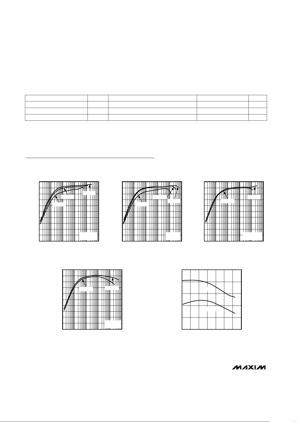
Typical Operating Characteristics
(L = 22µH, CIN= 47µF, C
OUT
= 47µF0.1µF, C
REF
= 0.1µF, TA= +25°C, unless otherwise noted.)
V
LBO
= 5.5V, V
LBI
= 5.5V
V
SHDN
= 0 or V
OUT
MAX1676, CLSEL = OUT
CONDITIONS
µA1I
LBO
LBO Off Leakage Current
nA75I
SHDN
SHDN Input Current
µA3I
CLSEL
CLSEL Input Current
UNITSMIN MAXSYMBOLPARAMETER
ELECTRICAL CHARACTERISTICS (continued)
(V
BATT
= 2V, FB = OUT, RL= ∞, TA= -40°C to +85°C, unless otherwise noted.) (Note 4)
Note 4: Specifications to -40°C are guaranteed by design, not production tested.
100
0
0.01 0.1 1 10 100 1000
EFFICIENCY vs. LOAD CURRENT
20
30
10
MAX1674 toc01
LOAD CURRENT (mA)
EFFICIENCY (%)
40
50
60
70
90
80
VIN = 1.2V
V
OUT
= 5V
I
LIMIT
= 500mA
VIN = 2.4V
VIN = 3.6V
100
0
0.01 0.1 1 10 100 1000
EFFICIENCY vs. LOAD CURRENT
20
30
10
MAX1674 toc02
LOAD CURRENT (mA)
EFFICIENCY (%)
40
50
60
70
90
80
VIN = 1.2V
V
OUT
= 5V
I
LIMIT
= 1A
VIN = 2.4V
VIN = 3.6V
100
0
0.01 0.1 1 10 100 1000
EFFICIENCY vs. LOAD CURRENT
20
30
10
MAX1674 toc03
LOAD CURRENT (mA)
EFFICIENCY (%)
40
50
60
70
90
80
VIN = 1.2V
V
OUT
= 3.3V
I
LIMIT
= 500mA
VIN = 2.4V
100
0
0.01 0.1 1 10 100 1000
EFFICIENCY vs. LOAD CURRENT
20
30
10
MAX1674 toc04
LOAD CURRENT (mA)
EFFICIENCY (%)
40
50
60
70
90
80
VIN = 1.2V
V
OUT
= 3.3V
I
LIMIT
= 1A
VIN = 2.4V
1.290
1.292
1.296
1.294
1.298
1.300
-40 0-20 20 40 60 80 100
REFERENCE OUTPUT VOLTAGE
vs. TEMPERATURE
MAX1674 toc05
TEMPERATURE (°C)
REFERENCE OUTPUT VOLTAGE (V)
I
REF
= 0
I
REF
= 100µA

MAX1674/MAX1675/MAX1676
High-Efficiency, Low-Supply-Current,
Compact, Step-Up DC-DC Converters
_______________________________________________________________________________________
5
0
40
20
100
80
60
140
120
160
0 1.5 2.00.5 1.0 2.5 3.0 3.5 4.0 4.5
NO-LOAD BATTERY CURRENT
vs. INPUT BATTERY VOLTAGE
MAX1674toc07
INPUT BATTERY VOLTAGE (V)
INPUT BATTERY CURRENT (µA)
I
LIMIT
= 1A, 5.0V
I
LIMIT
= 0.5A, 5.0V
I
LIMIT
= 0.5A, 3.3V
I
LIMIT
= 1A, 3.3V
1.8
0
0.01 1 100.1 100
START-UP VOLTAGE
vs. LOAD CURRENT
0.2
0.4
MAX1674toc08
LOAD CURRENT (mA)
START-UP VOLTAGE (V)
0.8
0.6
1.0
1.2
1.4
1.6
WITHOUT DIODE
WITH 1N5817
-1.0
-0.6
-0.8
-0.2
-0.4
0.2
0
0.4
0.8
0.6
1.0
1 2.0 2.5 3.01.5 3.5 4.0 4.5 5.0 5.5
SHUTDOWN CURRENT
vs. SUPPLY VOLTAGE
MAX167toc09
SUPPLY VOLTAGE (V)
SHUTDOWN CURRENT (µA)
0
0.4
0.2
0.8
0.6
1.2
1.0
1.4
0 1.0 1.50.5 2.0 2.5 3.0 3.5 4.0 4.5 5.0
SHUTDOWN THRESHOLD
vs. SUPPLY VOLTAGE
MAX1674TOC10
SUPPLY VOLTAGE (V)
SHUTDOWN THRESHOLD (V)
0
200
100
500
300
400
800
700
600
900
1.0 2.01.5 2.5 3.0 3.5 4.0 4.5
MAXIMUM OUTPUT CURRENT
vs. INPUT VOLTAGE (V
OUT
= 5V)
MAX1674toc11
INPUT VOLTAGE (V)
MAXIMUM OUTPUT CURRENT (mA)
1A CURRENT LIMIT
0.5A CURRENT LIMIT
0
200
100
400
300
600
500
800
700
1.0 1.4 1.61.2 1.8 2.0 2.2 2.4 2.6 2.8 3.0
MAXIMUM OUTPUT CURRENT
vs. INPUT VOLTAGE (V
OUT
= 3.3V)
MAX1674toc12
INPUT VOLTAGE (V)
MAXIMUM OUTPUT CURRENT (mA)
0.5A CURRENT LIMIT
1A CURRENT LIMIT
Typical Operating Characteristics (continued)
(L = 22µH, CIN= 47µF, C
OUT
= 47µF0.1µF, C
REF
= 0.1µF, TA= +25°C, unless otherwise noted.)
1µs/div
HEAVY-LOAD SWITCHING WAVEFORMS
MAX1674 TOC13
V
LX
5V/div
I
LX
0.5A/div
V
OUT
AC COUPLED
100mV/div
V
IN
= 2.4V
V
OUT
= 5.0V
0
0.4
0.2
0.8
0.6
1.0
1.2
2.0 3.0 3.52.5 4.0 4.5 5.0
LX CURRENT LIMIT
vs. OUTPUT VOLTAGE
MAX1674toc14
OUTPUT VOLTAGE (V)
I
LIM
(A)
MAX1674, MAX1676 (CLSEL = OUT)
MAX1675, MAX1676 (CLSEL = GND)
0
0.15
0.10
0.05
0.25
0.20
0.35
0.30
0.45
0.40
-60 -20
-40
0 20 40 60 80 100
SWITCH RESISTANCE vs. TEMPERATURE
MAX1674toc13.5
TEMPERATURE (°C)
RESISTANCE (Ω)
P-CHANNEL
N-CHANNEL

10µs/div
LINE-TRANSIENT RESPONSE
MAX1674 TOC15
V
IN
2V TO 3V
1V/div
V
OUT
AC COUPLED
100mV/div
I
LOAD
100mA
5µs/div
LOAD-TRANSIENT RESPONSE
MAX1674 TOC16
I
OUT
200mA/div
V
OUT
50mV/div
AC
COUPLED
V
IN
= 2.4V
V
OUT
= 3.3V
500µs/div
EXITING SHUTDOWN
MAX1674 TOC17
V
SHDN
2V/div
V
OUT
2V/div
MAX1674/MAX1675/MAX1676
High-Efficiency, Low-Supply-Current,
Compact, Step-Up DC-DC Converters
6 _______________________________________________________________________________________
Typical Operating Characteristics (continued)
(L = 22µH, CIN= 47µF, C
OUT
= 47µF0.1µF, C
REF
= 0.1µF, TA= +25°C, unless otherwise noted.)
Pin Description
PIN
NAME FUNCTION
MAX1674
MAX1675
MAX1676
1 1 FB
Dual-Mode™ Feedback Input. Connect to GND for +5.0V output.
Connect to OUT for +3.3V output. Use a resistor network to set the
output voltage from +2.0V to +5.5V.
2 2 LBI Low-Battery Comparator Input. Internally set to trip at +1.30V.
3 3
LBO
Open-Drain Low-Battery Comparator Output. Output is low when
V
LBI
is <1.3V. LBO is high impedance during shutdown.
— 4 CLSEL
Current-Limit Select Input. CLSEL = OUT sets the current limit to 1A.
CLSEL = GND sets the current limit to 0.5A.
4 5 REF 1.3V Reference Voltage. Bypass with a 0.1µF capacitor.
5 6
SHDN
Shutdown Input. High = operating, low = shutdown.
— 7 BATT
Battery Input and Damping Switch Connection. If damping switch is
unused, leave BATT unconnected.
6 8 GND Ground
7 9 LX N-Channel and P-Channel Power MOSFET Drain
8 10 OUT Power Output. OUT provides bootstrap power to the IC.
Dual-Mode is a trademark of Maxim Integrated Products.

Detailed Description
The MAX1674/MAX1675/MAX1676 compact, step-up
DC-DC converters start up with voltages as low as 0.9V
and operate with an input voltage down to 0.7V.
Consuming only 16µA of quiescent current, these
devices offer a built-in synchronous rectifier that
reduces cost by eliminating the need for an external
diode and improves overall efficiency by minimizing
losses in the circuit (see
Synchronous Rectification
section for details). The internal MOSFET resistance is typically 0.3Ω, which minimizes losses. The current limit of
the MAX1674 and MAX1675 are 1A and 0.5A, respectively. The MAX1675’s lower current limit allows the use
of a physically smaller inductor in space-sensitive
applications. The MAX1676 features a circuit that eliminates noise due to inductor ringing. In addition, the
MAX1676 offers a selectable current limit (0.5A or 1A)
for design flexibility.
PFM Control Scheme
A unique minimum-off-time, current-limited, pulse-frequency-modulation (PFM) control scheme is a key feature of the MAX1674/MAX1675/MAX1676. This scheme
combines the high output power and efficiency of a
pulse-width-modulation (PWM) device with the ultra-low
quiescent current of a traditional PFM (Figure 1). There
is no oscillator; a constant-peak-current limit in the
switch allows the inductor current to vary between this
peak limit and some lesser value. At light loads, the
switching frequency is governed by a pair of one-shots
that set a typical minimum off-time (1µs) and a typical
maximum on-time (4µs). The switching frequency
depends upon the load and the input voltage, and can
range up to 500kHz. The peak current of the internal Nchannel MOSFET power switch is fixed at 1A
(MAX1674), at 0.5A (MAX1675), or is selectable
(MAX1676). Unlike conventional pulse-skipping DC-DC
converters (where ripple amplitude varies with input
voltage), ripple in these devices does not exceed the
product of the switch current limit and the filter-capacitor equivalent series resistance (ESR).
Synchronous Rectification
The internal synchronous rectifier eliminates the need
for an external Schottky diode, thus reducing cost and
board space. During the cycle off-time, the P-channel
MOSFET turns on and shunts the MOSFET body diode.
MAX1674/MAX1675/MAX1676
High-Efficiency, Low-Supply-Current,
Compact, Step-Up DC-DC Converters
_______________________________________________________________________________________ 7
MAX1674
MAX1675
MAX1676
ONE-SHOT
TRIG
Q
F/F
R
S
Q
ONE-SHOT
TRIG
Q
CURRENT-LIMIT
AMPLIFIER
ERROR
AMPLIFIER
LOW-BATTERY
COMPARATOR
REFERENCE
REF
FB
V
IN
47µF
47µF
R1
200Ω
R5
R6
DAMPING
SWITCH
22µH
BATT
(MAX1676)
GND
LX
OUT
0.1µF
0.1µF
V
OUT
R4
LBI
LBO
R2
100k
R3
V
IN
V
OUT
CLSEL
(MAX1676)
SHDN
MINIMUM
OFF-TIME
ONE-SHOT
ZERO
CROSSING
AMPLIFIER
EN
MAXIMUM
ON-TIME
ONE-SHOT
P
N
Figure 1. Simplified Functional Diagram

MAX1674/MAX1675/MAX1676
As a result, the synchronous rectifier significantly
improves efficiency without the addition of an external
component. Conversion efficiency can be as high as
94%, as shown in the
Typical Operating Characteristics
.
For low-voltage inputs from single cells (Alkaline, NiCd,
or NiMH), use an external Schottky diode such as the
1N5817 to ensure start-up.
Voltage Reference
The voltage at REF is nominally +1.30V. REF can
source up to 100µA to external circuits. The reference
maintains excellent load regulation (see
Typical Oper-
ating Characteristics
). A bypass capacitor of 0.1µF is
required for proper operation.
Shutdown
The device enters shutdown when V
SHDN
is low.
During shutdown, the body diode of the P-channel
MOSFET allows current flow from the battery to the output. V
OUT
falls to approximately VIN- 0.6V and LX
remains high impedance. The capacitance and load at
OUT determine the rate at which V
OUT
decays.
Shutdown can be pulled as high as 6V, regardless of
the voltage at OUT.
Current Limit Select Pin (MAX1676)
The MAX1676 allows a selectable inductor current limit
of either 0.5A or 1A. This allows flexibility in designing
for higher current applications or for smaller, compact
designs. Connect CLSEL to OUT for 1A or to GND for
0.5A. CLSEL draws 1.4µA when connected to OUT.
BATT/Damping Switch (MAX1676)
The MAX1676 is designed with an internal damping
switch to minimize ringing at LX. The damping switch
connects an external resistor (R1) across the inductor
when the inductor’s energy is depleted (Figure 2).
Normally, when the energy in the inductor is insufficient
to supply current to the output, the capacitance and
inductance at LX form a resonant circuit that causes
ringing. The ringing continues until the energy is dissipated through the series resistance of the inductor. The
damping switch supplies a path to quickly dissipate this
energy, minimizing the ringing at LX. Damping LX ringing does not reduce V
OUT
ripple, but does reduce EMI.
R1 = 200Ω works well for most applications while reducing efficiency by only 1%. Larger R1 values provide less
damping, but have less impact on efficiency. Generally,
lower values of R1 are needed to fully damp LX when
the V
OUT/VIN
ratio is high (Figures 2, 3, and 4).
High-Efficiency, Low-Supply-Current,
Compact, Step-Up DC-DC Converters
8 _______________________________________________________________________________________
MAX1676
DAMPING
SWITCH
BATT
R1
200Ω
LX
OUT
22µH
V
IN
0.1µF
47µF
V
OUT
Figure 2. Simplified Diagram of Inductor Damping Switch
2µs/div
V
LX
1V/div
Figure 3. LX Ringing Without Damping Switch
2µs/div
V
LX
1V/div
Figure 4. LX Waveform with Damping Switch (with 200
Ω
external resistor)

Selecting the Output Voltage
V
OUT
can be set to 3.3V or 5.5V by connecting the FB
pin to GND (5V) or OUT (3.3V) (Figures 5 and 6).
To adjust the output voltage, connect a resistor-divider
from V
OUT
to FB to GND (Figure 7). Choose a value
less than 260kΩ for R6. Use the following equation to
calculate R5:
R5 = R6 [(V
OUT
/ V
REF
) - 1]
where V
REF
= +1.3V and V
OUT
may range from 2V to
5V. The input bias current of FB has a maximum value
of 50nA which allows large-value resistors (R6 ≤ 260kΩ)
to be used.
Low-Battery Detection
The MAX1674/MAX1675/MAX1676 contain an on-chip
comparator for low-battery detection. If the voltage at
LBI falls below the internal reference voltage (1.30V),
LBO (an open-drain output) sinks current to GND. The
low-battery monitor threshold is set by two resistors, R3
and R4 (Figures 5, 6, and 7). Since the LBI current is
less than 50nA, large resistor values (R4 ≤ 260kΩ) can
be used to minimize loading of the input supply.
Calculate R3 using the following equation:
R3 = R4 [(V
TRIP
/ V
REF
) - 1]
for V
TRIP
≥ 1.3V. V
TRIP
is the level where the low-battery
detector output goes low, and V
REF
is the internal
1.30V reference. Connect a pull-up resistor of 100kΩ or
greater from LBO to OUT when driving CMOS circuits.
LBO is an open-drain output, and can be pulled as
high as 6V regardless of the voltage at OUT. When LBI
is above the threshold, the LBO output is high impedance. If the low-battery comparator is not used, ground
MAX1674/MAX1675/MAX1676
High-Efficiency, Low-Supply-Current,
Compact, Step-Up DC-DC Converters
_______________________________________________________________________________________ 9
MAX1674
MAX1675
MAX1676
BATT
(MAX1676)
V
IN
LBI
REF
GND
R3
R1
200Ω
R4
R2
100k
47µF
10V
22µH
0.1µF
LX
LBO
0.1µF
47µF
+3.3V
200mA
V
OUT
LOW-BATTERY
OUTPUT
FB
SHDN
OUT
CLSEL
(MAX1676)
Figure 5. Preset Output Voltage of +3.3V
MAX1674
MAX1675
MAX1676
BATT
(MAX1676)
V
IN
LBI
REF
GND
R6
R5
R3
R1
200Ω
R4
R2
100k
22µH
47µF
0.1µF
LX
LBO
OUTPUT
2V to 5.5V
FB
SHDN
OUT
CLSEL
(MAX1676)
LOWBATTERY
OUTPUT
0.1µF
47µF
Figure 7. Setting an Adjustable Output
MAX1674
MAX1675
MAX1676
BATT
(MAX1676)
V
IN
LBI
REF
GND
R3
R1
200Ω
R4
R2
100k
22µH
47µF
0.1µF
LX
LBO
0.1µF
47µF
OUTPUT
5.0V,
150mA
FB
SHDN
OUT
CLSEL
(MAX1676)
LOWBATTERY
OUTPUT
Figure 6. Preset Output Voltage of +5V

MAX1674/MAX1675/MAX1676
LBI and LBO. For V
TRIP
less than 1.3V, configure the
comparator as shown in Figure 8. Calculate the value of
the external resistors R3 and R4 as follows:
R3 = R4(V
REF
- V
TRIP
) / (V
OUT
- V
REF
)
Since the low-battery comparator is noninverting, external hysteresis can be added by connecting a resistor
between LBO and LBI as shown in Figure 9. When LBO
is high, the series combination of R2 and R7 source
current into the LBI summing junction.
Applications Information
Inductor Selection
An inductor value of 22µH performs well in most applications. The MAX1674/MAX1675/MAX1676 will also
work with inductors in the 10µH to 47µH range. Smaller
inductance values typically offer a smaller physical size
for a given series resistance, allowing the smallest
overall circuit dimensions. However, due to higher peak
inductor currents, the output voltage ripple (I
PEAK
x
output filter capacitor ESR) also tends to be higher.
Circuits using larger inductance values exhibit higher
output current capability and larger physical dimensions for a given series resistance. The inductor’s incremental saturation current rating should be greater than
the peak switch-current limit, which is 1A for the
MAX1674, 500mA for the MAX1675, and 1A or 0.5A for
the MAX1676. However, it is generally acceptable to
bias the inductor into saturation by as much as 20%,
although this will slightly reduce efficiency. Table 1 lists
suggested components.
The inductor’s DC resistance significantly affects efficiency. See Table 2 for a comparison of inductor specifications. Calculate the maximum output current as
follows:
where I
OUT(MAX)
= maximum output current in amps
V
BATT
= input voltage
L = inductor value in µH
η= efficiency (typically 0.9)
t
OFF
= LX switch’s off-time in µs
RP= resistance of P-channel MOSFET in Ω
I
LIM
= 0.5A or 1.0A
I
V I
V V
L
t
R
V
OUT MAX
BATT LIM
OUT BATT
OFF
P
OUT
( )
=
+
– /
–
1 2 η
High-Efficiency, Low-Supply-Current,
Compact, Step-Up DC-DC Converters
10 ______________________________________________________________________________________
MAX1674
MAX1675
MAX1676
BATT
(MAX1676)
V
IN
LBI
REF
GND
R3
R1
200Ω
R4
22µH
47µF
0.1µF
LX
LBO
V
OUT
FB
R2
100k
SHDN
OUT
CLSEL
(MAX1676)
LOWBATTERY
OUTPUT
0.1µF
47µF
Figure 8. Setting Resistor Values for the Low-Battery Indicator
when V
IN
< 1.3V
MAX1674
MAX1675
MAX1676
LBI
GND
V
TRIP
(VH, VL)
R3
R4
R7
V
H
IS THE UPPER TRIP LEVEL
VL IS THE LOWER TRIP LEVEL
WHERE
R2
100k
LBO
OUT
V
OUT
0.1µF
47µF
V = 1.3V
V = 1.3V
H
L
( )
+ +
( )
+ −
−
+
( . )
( . ) ( )
1
373
4
1
3
4
1 3 3
1 3 2 7
RRR
R
R
R
V V R
V R R
OUT
Figure 9. Adding External Hysteresis to the Low-Battery
Indicator

Capacitor Selection
A 47µF, 10V surface-mount tantalum (SMT) output filter
capacitor provides 80mV output ripple when stepping
up from 2V to 5V. Smaller capacitors (down to 10µF
with higher ESRs) are acceptable for light loads or in
applications that can tolerate higher output ripple.
Values in the 10µF to 100µF range are recommended.
The equivalent series resistance (ESR) of both bypass
and filter capacitors affects efficiency and output ripple. Output voltage ripple is the product of the peak
inductor current and the output capacitor ESR. Use
low-ESR capacitors for best performance, or connect
two or more filter capacitors in parallel. Low-ESR, SMT
tantalum capacitors are currently available from
Sprague (595D series) AVX (TPS series) and other
sources. Ceramic surface-mount and Sanyo OS-CON
organic-semiconductor through-hole capacitors also
exhibit very low ESR, and are especially useful for operation at cold temperatures. See Table 3 for a list of suggested component suppliers.
MAX1674/MAX1675/MAX1676
High-Efficiency, Low-Supply-Current,
Compact, Step-Up DC-DC Converters
______________________________________________________________________________________ 11
PRODUCTION
METHOD
INDUCTORS CAPACITORS
RECTIFIERS
(OPTIONAL)
Surface Mount
Sumida CD43 series
Sumida CD54 series
Coilcraft DT1608C
Coilcraft DO1608C
Coiltronics Uni-PAC
Murata LQH4 series
Sprague 593D series
Sprague 595D series
AVX TPS series
ceramic
Motorola MBR0530
Nihon EC 15QS02L
Miniature Through-Hole Sumida RCH654-220 Sanyo OS-CON series —
Table 1. Suggested Components
Table 2. Surface-Mount Inductor
Specifications
MANUFACTURER
PART NUMBER
µH Ω (max) I
PEAK
(A)
HEIGHT
(mm)
Coilcraft DT1608C-103 10 0.095 0.7 2.92
Coilcraft DO1608C-153 15 0.200 0.9 2.92
Coilcraft DO1608C-223 22 0.320 0.7 2.92
Coiltronics UP1B-100 10 0.111 1.9 5.0
Table 3. Component Suppliers
COMPANY PHONE FAX
AVX USA (803) 946-0690 USA (803) 626-3123
Coilcraft USA (847) 639-6400 USA (847) 639-1469
Coiltronics USA (561) 241-7876 USA (561) 241-9339
Murata
USA (814) 237-1431
(800) 831-9172
USA (814) 238-0490
Nihon
USA (805) 867-2555
Japan 81-3-3494-7411
USA (805) 867-2556
Japan 81-3-3494-7414
Motorola
USA (303) 675-2140
(800) 521-6274
USA (303) 675-2150
Sanyo
USA (619) 661-6835
Japan 81-7-2070-6306
USA (619) 661-1055
Japan 81-7-2070-1174
Sumida
USA (647) 956-0666
Japan 81-3-3607-5111
USA (647) 956-0702
Japan 81-3-3607-5144
Taiyo Yuden USA (408) 573-4150 USA (408) 573-4159
Sprague USA (603) 224-1961 USA (603) 224-1430
Coiltronics UP1B-150 15 0.175 1.5 5.0
Coiltronics UP1B-220 22 0.254 1.2 5.0
Murata LQH4N100 10 0.560 0.4 2.6
Murata LQH4N220 22 0.560 0.4 2.6
Sumida CD43-8R2 8.2 0.132 1.26 3.2
Sumida CD43-100 10 0.182 1.15 3.2
Sumida CD54-100 10 0.100 1.44 4.5
Sumida CD54-180 18 0.150 1.23 4.5
Sumida CD54-220 22 0.180 1.11 4.5

MAX1674/MAX1675/MAX1676
High-Efficiency, Low-Supply-Current,
Compact, Step-Up DC-DC Converters
12 ______________________________________________________________________________________
TRANSISTOR COUNT: 751
Chip Information
Package Information
Optional External Rectifier
Although not required, a Schottky diode (such as the
MBR0520) connected between LX and OUT allows
lower start-up voltages (Figure 10) and is recommended for single-cell operation. Note that adding this diode
provides no significant efficiency improvement.
PC Board Layout and Grounding
Careful printed circuit layout is important for minimizing
ground bounce and noise. Keep the IC’s GND pin and
the ground leads of the input and output filter capacitors less than 0.2in (5mm) apart. In addition, keep all
connections to the FB and LX pins as short as possible. In particular, when using external feedback resistors, locate them as close to the FB as possible. To
maximize output power and efficiency and minimize
output ripple voltage, use a ground plane and solder
the IC’s GND directly to the ground plane.
MAX1674
MAX1675
MAX1676
BATT
(MAX1676)
V
IN
SINGLE CELL
LBI
REF
GND
R3
R1
200Ω
R4
R2
100k
22µH
47µF
0.1µF
LX
LBO
FB
SHDN
OUT
LOW-BATTERY
OUTPUT
0.1µF
MBR0520
47µF
CLSEL
(MAX1676)
Figure 10. Adding a Schottky Diode for Single-Cell Operation
10LUMAXB.EPS
 Loading...