Maxim MAX1676EUA, MAX1675EUA, MAX1674EUA Datasheet

For free samples & the latest literature: http://www.maxim-ic.com, or phone 1-800-998-8800.
For small orders, phone 408-737-7600 ext. 3468.
General Description
The MAX1674/MAX1675/MAX1676 compact, high-efficiency, step-up DC-DC converters fit in small µMAX
packages. They feature a built-in synchronous rectifier,
which improves efficiency and reduces size and cost
by eliminating the need for an external Schottky diode.
Quiescent supply current is only 16µA.
The input voltage ranges from 0.7V to V
OUT
, where
V
OUT
can be set from 2V to 5.5V. Start-up is guaranteed from 1.1V inputs. The MAX1674/MAX1675/
MAX1676 have a preset, pin-selectable output for 5V or
3.3V. The outputs can also be adjusted to other voltages using two external resistors.
All three devices have a 0.3Ω N-channel MOSFET
power switch. The MAX1674 has a 1A current limit. The
MAX1675 has a 0.5A current limit, which permits the
use of a smaller inductor. The MAX1676 comes in a
10-pin µMAX package and features an adjustable current limit and circuitry to reduce inductor ringing.
________________________Applications
Pagers
Wireless Phones
Medical Devices
Hand-Held Computers
PDAs
RF Tags
1 to 3-Cell Hand-Held Devices
____________________________Features
♦ 94% Efficient at 200mA Output Current
♦ 16µA Quiescent Supply Current
♦ Internal Synchronous Rectifier (no external diode)
♦ 0.1µA Logic-Controlled Shutdown
♦ LBI/LBO Low-Battery Detector
♦ Selectable Current Limit for Reduced Ripple
♦ Low-Noise, Anti-Ringing Feature (MAX1676)
♦ 8-Pin and 10-Pin µMAX Packages
♦ Preassembled Evaluation Kit (MAX1676EVKIT)
MAX1674/MAX1675/MAX1676
High-Efficiency, Low-Supply-Current,
Compact, Step-Up DC-DC Converters
________________________________________________________________
Maxim Integrated Products
1
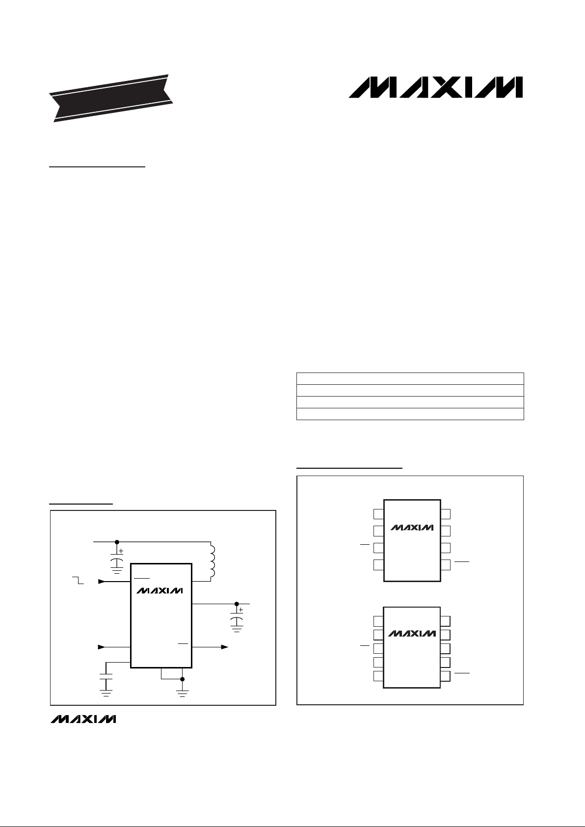
GNDLBO
SHDN
REF
1
2
8
7
OUT
LXLBI
FB
MAX1674
MAX1675
µMAX
TOP VIEW
3
4
6
5
1
2
3
4
5
10
9
8
7
6
OUT
LX
GND
BATTCLSEL
LBO
LBI
FB
MAX1676
µMAX
SHDNREF
MAX1674
MAX1675
INPUT
0.7V TO V
OUT
SHDN
LX
LBO
OUT
LBI
0.1µF
LOW-BATTERY
DETECT OUT
OFF
ON
REF
GND
FB
OUTPUT
3.3V, 5V, OR
ADJ (2V TO 5.5V)
UP TO 300mA
LOW-BATTERY
DETECT IN
PART
MAX1674EUA
-40°C to +85°C
TEMP. RANGE PIN-PACKAGE
8 µMAX
_______________Ordering Information
MAX1675EUA
-40°C to +85°C 8 µMAX
MAX1676EUB
-40°C to +85°C 10 µMAX
EVALUATION KIT
AVAILABLE
Typical Operating Circuit
Pin Configurations
19-1360; Rev 0; 7/98

MAX1674/MAX1675/MAX1676
High-Efficiency, Low-Supply-Current,
Compact, Step-Up DC-DC Converters
2 _______________________________________________________________________________________
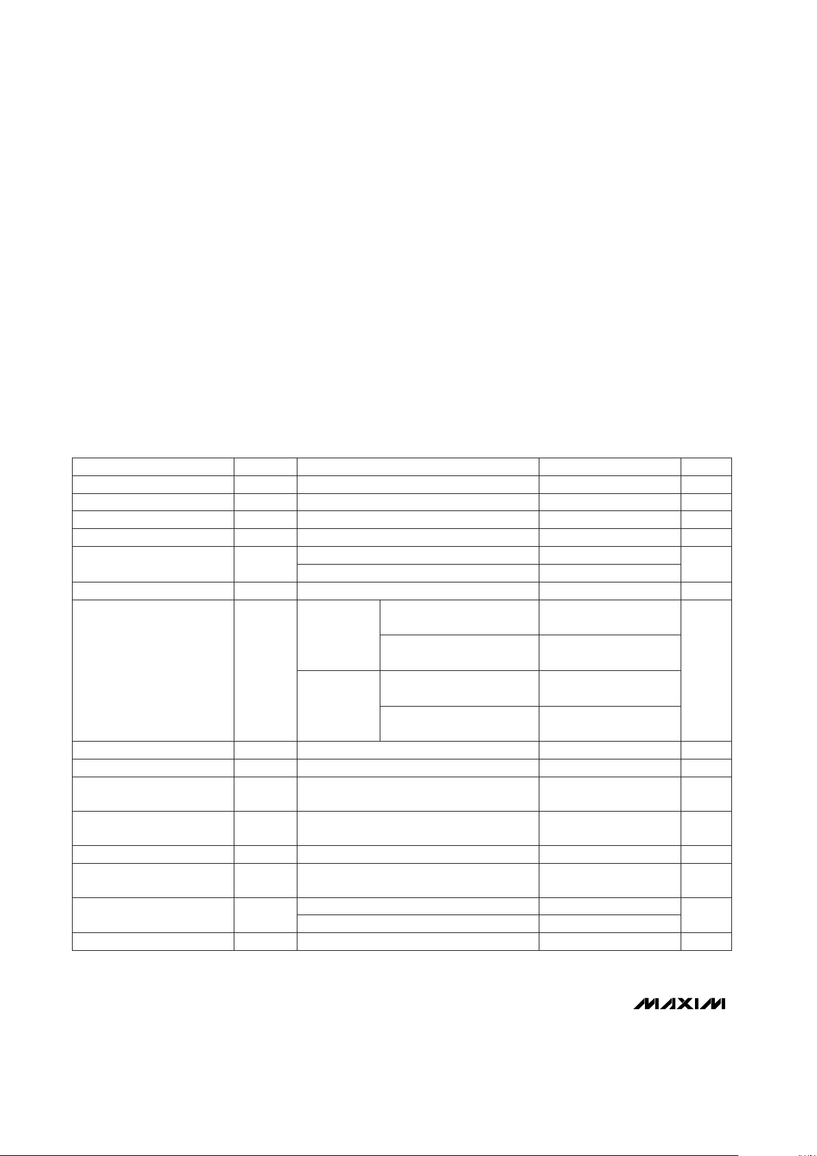
ABSOLUTE MAXIMUM RATINGS
ELECTRICAL CHARACTERISTICS
(V
BATT
= 2V, FB = OUT (V
OUT
= 3.3V), RL= ˙∞, TA= 0°C to +85°C, unless otherwise noted. Typical values are at TA= +25°C.)
Stresses beyond those listed under “Absolute Maximum Ratings” may cause permanent damage to the device. These are stress ratings only, and functional
operation of the device at these or any other conditions beyond those indicated in the operational sections of the specifications is not implied. Exposure to
absolute maximum rating conditions for extended periods may affect device reliability.
Supply Voltage (OUT to GND) ..............................-0.3V to +6.0V
Switch Voltage (LX to GND).....................-0.3V to (V
OUT
+ 0.3V)
Battery Voltage (BATT to GND).............................-0.3V to +6.0V
SHDN, LBO to GND ..............................................-0.3V to +6.0V
LBI, REF, FB, CLSEL to GND...................-0.3V to (V
OUT
+ 0.3V)
Switch Current (LX)...............................................-1.5A to +1.5A
Output Current (OUT) ...........................................-1.5A to +1.5A
Continuous Power Dissipation (T
A
= +70°C)
8-Pin µMAX (derate 4.1mW/°C above +70°C) .............330mW
10-Pin µMAX (derate 5.6mW/°C above +70°C) ...........444mW
Operating Temperature Range ...........................-40°C to +85°C
Junction Temperature......................................................+150°C
Storage Temperature Range.............................-65°C to +165°C
Lead Temperature (soldering, 10sec).............................+300°C
TA= +25°C, RL= 3kΩ (Note 1)
VLX= 0, 5.5V; V
OUT
= 5.5V
TA= +25°C
MAX1675, MAX1676 (CLSEL = GND)
MAX1674, MAX1676 (CLSEL = OUT)
ILX= 100mA
FB = OUT
(V
OUT
= 3.3V)
V
OUT
= 2V to 5.5V
I
REF
= 0 to 100µA
90 130
MAX1675,
MAX1676 (CLSEL = GND)
FB = OUT
FB = GND
I
REF
= 0
CONDITIONS
µA
0.05 1
I
LEAK
LX Leakage Current
A
0.4 0.5 0.65
I
LIM
0.80 1 1.20
LX Switch Current
Limit (NFET)
Ω
0.3 0.6
R
DS(ON)
Internal NFET, PFET
On-Resistance
V
1.274 1.30 1.326
FB, LBI Input Threshold
mV/V
0.08 2.5
V
REF_LINE
Reference Voltage Line
Regulation
mV
3 15
V
REF_LOAD
Reference Voltage Load
Regulation
mV/°C
0.024
TEMPCOReference Voltage Tempco
V
1.274 1.30 1.326
V
REF
Reference Voltage
V
0.9 1.1
Start-Up Voltage
V
1.1 5.5
V
IN
V
0.7
Minimum Input Voltage
Operating Voltage
150 220
FB = GND
(V
OUT
= 5V)
MAX1675,
MAX1676 (CLSEL = GND)
180 285
I
OUT
MAX1674,
MAX1676 (CLSEL = OUT)
mA
300 420
Steady-State Output Current
(Note 2)
mV/°C
-2
Start-Up Voltage Tempco
V
3.17 3.30 3.43
V
OUT
Output Voltage
4.80 5 5.20
MAX1674,
MAX1676 (CLSEL = OUT)
V
2 5.5
Output Voltage Range
UNITSMIN TYP MAXSYMBOLPARAMETER

MAX1674/MAX1675/MAX1676
High-Efficiency, Low-Supply-Current,
Compact, Step-Up DC-DC Converters
_______________________________________________________________________________________ 3
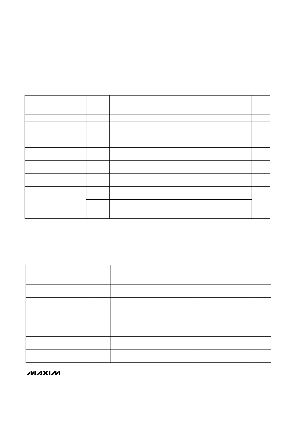
ELECTRICAL CHARACTERISTICS
(V
BATT
= 2V, FB = OUT, RL= ∞, TA= -40°C to +85°C, unless otherwise noted.) (Note 4)
Note 1: Start-up voltage operation is guaranteed with the addition of a Schottky MBR0520 external diode between the input and
output.
Note 2: Steady-state output current indicates that the device maintains output voltage regulation under load. See Figures 5 and 6.
Note 3: Device is bootstrapped (power to the IC comes from OUT). This correlates directly with the actual battery supply.
V
OUT
= 2V, I
LOAD
= 1mA
V
OUT
= 3.3V, I
LOAD
= 200mA
SHDN = GND
CONDITIONS
%
85
Efficiency
90
µA
0.1 1
Shutdown Current into OUT
UNITSMIN TYP MAXSYMBOLPARAMETER
MAX1676, V
BATT
= 2V
V
LBO
= 5.5V, V
LBI
= 5.5V
V
LBI
= 0, I
SINK
= 1mA
V
SHDN
= 0 or V
OUT
VFB= 1V, V
OUT
= 3.3V
MAX1676, CLSEL = OUT
V
LBI
= 1.4V
VFB= 1.4V
VFB= 1V, V
OUT
= 3.3V
0.8V
OUT
V
IH
0.2V
OUT
V
IL
CLSEL Input Voltage
V
0.8V
OUT
V
IH
0.2V
OUT
V
IL
SHDN Input Voltage
Ω88 150Damping Switch Resistance
µA
0.07 1
I
LBO
LBO Off Leakage Current
V
0.2 0.4
LBO Low Output Voltage
nA
0.07 50
I
SHDN
SHDN Input Current
µA
1.4 3
I
CLSEL
CLSEL Input Current
nA
1 50
I
LBI
LBI Input Current
nA
0.03 50
I
FB
FB Input Current
µs
0.8 1 1.2
t
OFF
LX Switch Off-Time
µs
3 4 7
t
ON
LX Switch On-Time
V
ELECTRICAL CHARACTERISTICS (continued)
(V
BATT
= 2V, FB = OUT (V
OUT
= 3.3V), RL= ˙∞, TA= 0°C to +85°C, unless otherwise noted. Typical values are at TA= +25°C.)
FB = GND
FB = OUT
VFB= 1V, V
OUT
= 3.3V
VFB= 1V, V
OUT
= 3.3V
SHDN = GND
VFB= 1.4V, V
OUT
= 3.3V
I
REF
= 0
MAX1675, MAX1676 (CLSEL = GND)
MAX1674, MAX1676 (CLSEL = OUT)
CONDITIONS
0.36 0.69
A
0.75 1.25
I
LIM
LX Switch Current
Limit (NFET)
V2.20 5.5Output Voltage Range
V
4.75 5.25
3.13 3.47
V
OUT
Output Voltage
µs0.75 1.25t
OFF
LX Switch Off-Time
µs2.7 7.0t
ON
LX Switch On-Time
µA1Shutdown Current into OUT
µA40
Operating Current into OUT
(Note 3)
V1.2675 1.3325V
REF
Reference Voltage
V1.2675 1.3325FB, LBI Thresholds
Ω0.6R
DS(ON)
Internal NFET, PFET
On-Resistance
UNITSMIN MAXSYMBOLPARAMETER
VFB= 1.4V, V
OUT
= 3.3V µA
16 35
Operating Current into OUT
(Note 3)

MAX1674/MAX1675/MAX1676
High-Efficiency, Low-Supply-Current,
Compact, Step-Up DC-DC Converters
4 _______________________________________________________________________________________
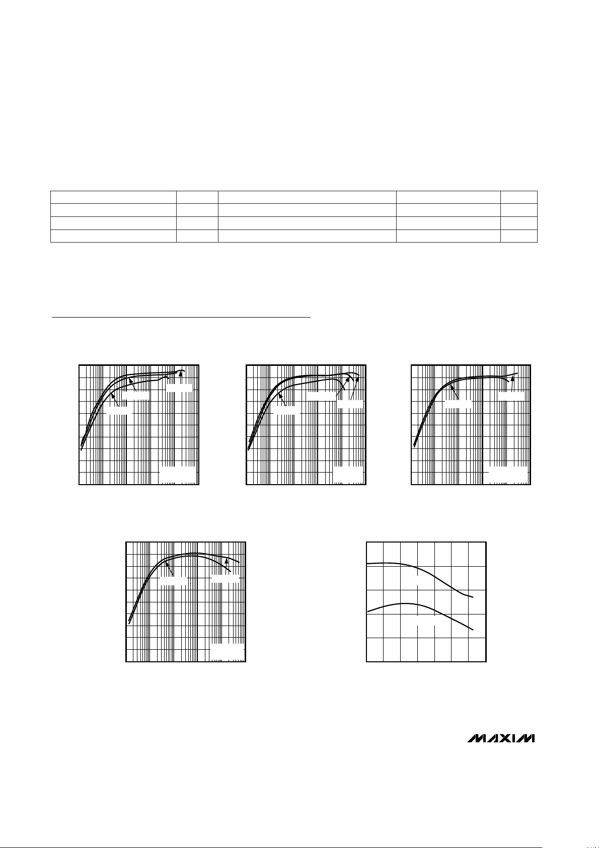
Typical Operating Characteristics
(L = 22µH, CIN= 47µF, C
OUT
= 47µF0.1µF, C
REF
= 0.1µF, TA= +25°C, unless otherwise noted.)
V
LBO
= 5.5V, V
LBI
= 5.5V
V
SHDN
= 0 or V
OUT
MAX1676, CLSEL = OUT
CONDITIONS
µA1I
LBO
LBO Off Leakage Current
nA75I
SHDN
SHDN Input Current
µA3I
CLSEL
CLSEL Input Current
UNITSMIN MAXSYMBOLPARAMETER
ELECTRICAL CHARACTERISTICS (continued)
(V
BATT
= 2V, FB = OUT, RL= ∞, TA= -40°C to +85°C, unless otherwise noted.) (Note 4)
Note 4: Specifications to -40°C are guaranteed by design, not production tested.
100
0
0.01 0.1 1 10 100 1000
EFFICIENCY vs. LOAD CURRENT
20
30
10
MAX1674 toc01
LOAD CURRENT (mA)
EFFICIENCY (%)
40
50
60
70
90
80
VIN = 1.2V
V
OUT
= 5V
I
LIMIT
= 500mA
VIN = 2.4V
VIN = 3.6V
100
0
0.01 0.1 1 10 100 1000
EFFICIENCY vs. LOAD CURRENT
20
30
10
MAX1674 toc02
LOAD CURRENT (mA)
EFFICIENCY (%)
40
50
60
70
90
80
VIN = 1.2V
V
OUT
= 5V
I
LIMIT
= 1A
VIN = 2.4V
VIN = 3.6V
100
0
0.01 0.1 1 10 100 1000
EFFICIENCY vs. LOAD CURRENT
20
30
10
MAX1674 toc03
LOAD CURRENT (mA)
EFFICIENCY (%)
40
50
60
70
90
80
VIN = 1.2V
V
OUT
= 3.3V
I
LIMIT
= 500mA
VIN = 2.4V
100
0
0.01 0.1 1 10 100 1000
EFFICIENCY vs. LOAD CURRENT
20
30
10
MAX1674 toc04
LOAD CURRENT (mA)
EFFICIENCY (%)
40
50
60
70
90
80
VIN = 1.2V
V
OUT
= 3.3V
I
LIMIT
= 1A
VIN = 2.4V
1.290
1.292
1.296
1.294
1.298
1.300
-40 0-20 20 40 60 80 100
REFERENCE OUTPUT VOLTAGE
vs. TEMPERATURE
MAX1674 toc05
TEMPERATURE (°C)
REFERENCE OUTPUT VOLTAGE (V)
I
REF
= 0
I
REF
= 100µA
 Loading...