

General Description
The MAX1667 provides the power control necessary to
charge batteries of any chemistry. All charging functions
are controlled through the Intel System Management Bus
(SMBus™) interface. The SMBus 2-wire serial interface
sets the charge voltage and current and provides thermal
status information. The MAX1667 functions as a Level 2
charger, compliant with the Duracell/Intel Smart Battery
Charger Specification.
In addition to the feature set required for a Level 2 charger, the MAX1667 generates interrupts to signal the host
when power is applied to the charger or when a battery is
installed or removed. Additional status bits allow the host
to check whether the charger has enough input voltage,
and whether the voltage on or current into the battery is
being regulated. This allows the host to determine when
lithium-ion (Li+) batteries have completed the charge without interrogating the battery.
The MAX1667 is available in a 20-pin SSOP with a 2mm
profile height.
________________________Applications
Notebook Computers Charger Base Stations
Personal Digital Assistants Phones
____________________________Features
♦ Charges Any Battery Chemistry: Li+, NiCd,
NiMH, Lead Acid, etc.
♦ SMBus 2-Wire Serial Interface
♦ Compliant with Duracell/Intel Smart Battery
Charger Specification Rev. 1.0
♦ 4A, 3A, or 1A (max) Battery Charge Current
♦ 5-Bit Control of Charge Current
♦ Up to 18.4V Battery Voltage
♦ 11-Bit Control of Voltage
♦ ±1% Voltage Accuracy
♦ Up to +28V Input Voltage
♦ Battery Thermistor Fail-Safe Protection
♦ Greater than 95% Efficiency
♦ Synchronous Rectifier
MAX1667
Chemistry-Independent,
Level 2 Smart Battery Charger
________________________________________________________________
Maxim Integrated Products
1
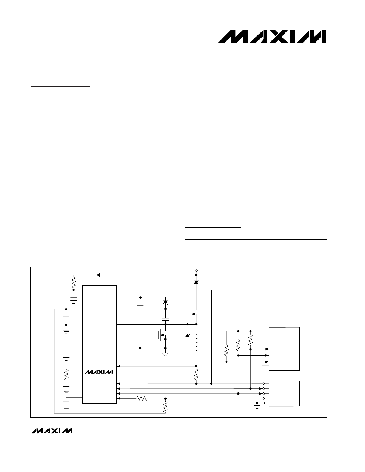
Typical Operating Circuit
PART
MAX1667EAP -40°C to +85°C
TEMP. RANGE PIN-PACKAGE
20 SSOP
Ordering Information
For free samples & the latest literature: http://www.maxim-ic.com, or phone 1-800-998-8800.
For small orders, phone 1-800-835-8769.
SMBus is a trademark of Intel Corp.
19-1488; Rev 0; 7/99
MAX1667
DCIN
REF BST
DHI
LX
DLO
PGND
INT
CS
BATT
SCL
SDA
THM
IOUT
VL
CHARGE SOURCE
AGND
SEL
DACV
CCV
CCI
V
DD
HOST
CONTROLLER
SMART
BATTERY
SCL
SDA
INT
GND
BATT+
R
SENSE
SCL
SDA
TEMP
BATT-
Pin Configuration appears at end of data sheet.
MAX1667
Chemistry-Independent,
Level 2 Smart Battery Charger
2 _______________________________________________________________________________________
ABSOLUTE MAXIMUM RATINGS
ELECTRICAL CHARACTERISTICS
(V
DCIN
= 18V, internal reference, 1µF capacitor at REF, 1µF capacitor at VL, TA= 0°C to +85°C, unless otherwise noted. Typical values
are at T
A
= +25°C, unless otherwise noted.)
Stresses beyond those listed under “Absolute Maximum Ratings” may cause permanent damage to the device. These are stress ratings only, and functional
operation of the device at these or any other conditions beyond those indicated in the operational sections of the specifications is not implied. Exposure to
absolute maximum rating conditions for extended periods may affect device reliability.
DCIN to AGND .......................................................-0.3V to +30V
BST to AGND..........................................................-0.3V to +36V
BST, DHI to LX..........................................................-0.3V to +6V
LX, IOUT to AGND..................................................-0.3V to +30V
THM, CCI, CCV, DACV, REF,
DLO to AGND .............................................-0.3V to (VL + 0.3V)
VL, SEL, INT, SDA, SCL to AGND............................-0.3V to +6V
BATT, CS+ to AGND ..............................................-0.3V to +20V
PGND to AGND.....................................................-0.3V to +0.3V
SDA, INT Current ................................................................50mA
VL Current...........................................................................50mA
Continuous Power Dissipation (T
A
= +70°C)
SSOP (derate 8mW/°C above +70°C) ..........................640mW
Operating Temperature Range ...........................-40°C to +85°C
Storage Temperature Range .............................-60°C to +150°C
Lead Temperature (soldering, 10sec) .............................+300°C
%
-0.8 0.8
ChargingVoltage()
= 0x3130 (12,592mV)
and
0x41A0 (16,800mV)
Voltage Accuracy
mV5ChargingCurrent() = 0x0080 (128mA)
CS to BATT Single-Count
Current-Sense Voltage
V019BATT, CS Input Voltage Range
µA
350 500VL > 5.15V, V
BATT
= 12V
BATT Input Current (Note 1)
15VL < 3.2V, V
BATT
= 12V
Ω58High or lowDLO On-Resistance
Ω47High or lowDHI On-Resistance
mA467.5V < V
DCIN
< 28V, logic inputs = VLDCIN Quiescent Current
V7.5 28DCIN Input Voltage Range
%96.5 97.7In dropoutDHI Maximum Duty Cycle
kHz200 250 300Not in dropoutOscillator Frequency
V5.15 5.4 5.657.5V < V
DCIN
< 28V, no loadVL Output Voltage
mV100I
LOAD
= 0 to 10mAVL Load Regulation
V3.20 4 5.15VL AC_PRESENT Trip Point
4.055 4.096 4.137
UNITSMIN TYP MAXCONDITIONSPARAMETER
µA
170 400VL > 5.15V, VCS= 12V
CS Input Current (Note 1)
15VL < 3.2V, VCS= 12V
mV145 160 175
SEL = VL (4A),
ChargingCurrent() = 0x0F80 (3968mA)
CS to BATT Full-Scale
Current-Sense Voltage
V0 < I
SOURCE
< 500µAREF Output Voltage
TA= +25°C
TA= T
MIN
to T
MAX
-1.0 1.0
TA= +25°C
TA= T
MIN
to T
MAX
-3.0 3.0
-1.0 1.0
ChargingVoltage()
= 0x1060 (4192mV)
and
0x20D0 (8400mV)
SWITCHING REGULATOR
SUPPLY AND REFERENCE
MAX1667
Chemistry-Independent,
Level 2 Smart Battery Charger
_______________________________________________________________________________________ 3
ELECTRICAL CHARACTERISTICS (continued)
(V
DCIN
= 18V, internal reference, 1µF capacitor at REF, 1µF capacitor at VL, TA= 0°C to +85°C, unless otherwise noted. Typical values
are at T
A
= +25°C, unless otherwise noted.)
Note 1: When DCIN is less than 4V, VL is less than 3.2V, causing the battery current to be typically 2µA (CS plus BATT input
current).
Bits11Guaranteed monotonicVDAC Voltage-Setting DAC Resolution
Bits5Guaranteed monotonicCDAC Current-Setting DAC Resolution
mA5
mA579
% of
V
REF
3 4.5 6THM falling
THM THERMISTOR_UR
Underrange Trip Point
% of
V
REF
22 23.5 25THM falling
THM THERMISTOR_HOT
Trip Point
% of
V
REF
74 75.5 77THM falling
THM THERMISTOR_COLD
Trip Point
mA/V0.2GMI Amplifier Transconductance
mA/V1.4GMV Amplifier Transconductance
% of
V
REF
89 91 93THM falling
THM THERMISTOR_OR
Overrange Trip Point
% of
V
DCIN
93 95 97BATT risingBATT POWER_FAIL Threshold
µA±80
GMV Amplifier Maximum
Output Current
µA±200
GMI Amplifier Maximum
Output Current
mV25 80 2001.1V < V
CCI
< 3.5V
CCV Clamp Voltage with
Respect to CCI
UNITSMIN TYP MAXCONDITIONSPARAMETER
mA6V
SDA
= 0.6VSDA Output Low Sink Current
µA-1 1SDA, SCL Input Bias Current
V2.2SDA, SCL Input Voltage High
V0.8SDA, SCL Input Voltage Low
mV25 80 2001.1V < V
CCV
< 3.5V
CCI Clamp Voltage with
Respect to CCV
ChargingCurrent() = 0x0000 10 µA
ChargingCurrent() = 0x0001
to 0x007F (127mA)
V
IOUT
= 17V, ChargingCurrent() = 0x0001
to 0x007F (127mA)
V
DCIN
= 0, V
IOUT
= 20V µA10IOUT Leakage Current
V
IOUT
= 0
IOUT Output Current
% of
V
DCIN
0.5
THM THERMISTOR_OR, _COLD,
_HOT, _UR Trip Point Hysteresis
% of
V
DCIN
1
BATT POWER_FAIL Threshold
Hysteresis
ERROR AMPLIFIERS
TRIP POINTS AND LINEAR CURRENT SOURCES
CURRENT- AND VOLTAGE-SETTING DACs
LOGIC LEVELS
MAX1667
Chemistry-Independent,
Level 2 Smart Battery Charger
4 _______________________________________________________________________________________
ELECTRICAL CHARACTERISTICS
(V
DCIN
= 18V, internal reference, 1µF capacitor at REF, 1µF capacitor at VL, TA= -40°C to +85°C, unless otherwise noted. Typical values
are at T
A
= +25°C. Limits over this temperature range are guaranteed by design.)
µACS Input Current (Note 1) 5VL < 3.2V, VCS= 12V
mV145 160 175
V
SEL
= VL,
ChargingCurrent() = 0x0F80 (128mA)
CS to BATT Full-Scale
Current-Sense Voltage
%
-1.0 1.0
ChargingVoltage() = 0x3130 (12,592mV),
ChargingVoltage() = 0x41A0 (16,800mV)
Voltage Accuracy
µABATT Input Current (Note 1) 5VL < 3.2V, V
BATT
= 12V
Ω58High or lowDLO On-Resistance
Ω47High or lowDHI On-Resistance
mA467.5V < V
DCIN
< 28V, logic inputs = VLDCIN Quiescent Current
%96.5In dropoutDHI Maximum Duty Cycle
kHz200 250 310Not in dropoutOscillator Frequency
V5.15 5.4 5.657.5V < V
DCIN
< 28V, no loadVL Output Voltage
V4.055 4.1370 < I
SOURCE
< 500µAREF Output Voltage
UNITSMIN TYP MAXCONDITIONSPARAMETER
% of
V
REF
88.5 93.5THM falling
THM THERMISTOR_OR
Overrange Trip Point
% of
V
REF
73.5 77.5THM falling
THM THERMISTOR_COLD
Trip Point
V0.5SDA, SCL Input Voltage Low
V2.2SDA, SCL Input Voltage High
µA-1 1SDA, SCL Input Bias Current
% of
V
REF
21.5 25.5THM falling
THM THERMISTOR_HOT
Trip Point
% of
V
REF
2.5 6.5THM falling
THM THERMISTOR_UR
Underrange Trip Point
mA6V
SDA
= 0.6VSDA Output Low Sink Current
%1
THM THERMISTOR_OR, _COLD,
_HOT, _UR Trip Point Hysteresis
-3.0 3.0
ChargingVoltage() = 0x1060 (4192mV),
ChargingVoltage() = 0x20D0 (8400mV)
SUPPLY AND REFERENCE
SWITCHING REGULATOR
TRIP POINTS AND LINEAR CURRENT SOURCES
LOGIC LEVELS
MAX1667
Chemistry-Independent,
Level 2 Smart Battery Charger
_______________________________________________________________________________________ 5
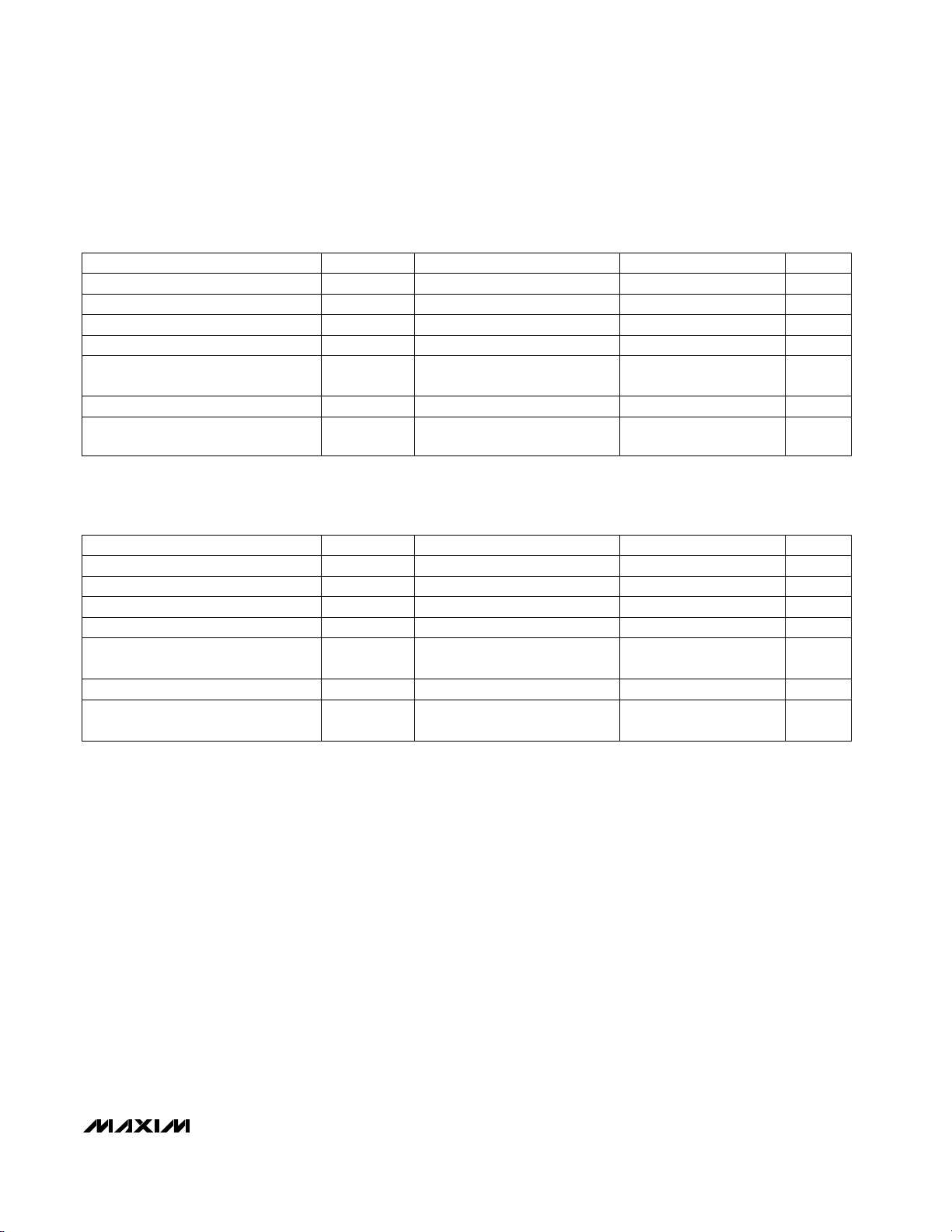
TIMING CHARACTERISTICS (Figures 1 and 2)
(TA= 0°C to +85°C, unless otherwise noted.)
TIMING CHARACTERISTICS (Figures 1 and 2)
(TA= -40°C to +85°C, unless otherwise noted. Limits over this temperature range are guaranteed by design.)
CONDITIONS
µs1t
DV
SCL Falling Edge to SDA Valid,
Master Clocking in Data
ns0t
HD:DAT
SCL Falling Edge to SDA Transition
µs4.7t
SU:STA
Start-Condition Setup Time
µs4.7t
LOW
µs4t
HIGH
SCL Serial-Clock High Period
SCL Serial-Clock Low Period
µs4t
HD:STA
Start-Condition Hold Time
ns250t
SU:DAT
SDA Valid to SCL Rising-Edge
Setup Time, Slave Clocking in Data
UNITSMIN TYP MAXSYMBOLPARAMETER
CONDITIONS
µs4.7t
SU:STA
Start-Condition Setup Time
µs4.7t
LOW
UNITSMIN TYP MAXSYMBOLPARAMETER
SCL Serial-Clock Low Period
µs4t
HD:STA
Start-Condition Hold Time
µs4t
HIGH
SCL Serial-Clock High Period
ns250t
SU:DAT
SDA Valid to SCL Rising-Edge
Setup Time, Slave Clocking in Data
ns0t
HD:DAT
SCL Falling Edge to SDA Transition
µs1t
DV
SCL Falling Edge to SDA Valid,
Master Clocking in Data
MAX1667
Chemistry-Independent,
Level 2 Smart Battery Charger
6 _______________________________________________________________________________________
Figure 2. SMBus Serial-Interface Timing—Acknowledge
t
DV
SLAVE PULLING
SDA LOW
t
DV
MOST SIGNIFICANT BIT
OF DATA CLOCKED
INTO MASTER
ACKNOWLEDGE
BIT CLOCKED
INTO MASTER
RW BIT
CLOCKED
INTO SLAVE
SCL
SDA
START
CONDITION
MOST SIGNIFICANT
ADDRESS BIT (A6)
CLOCKED INTO SLAVE
A5 CLOCKED
INTO SLAVE
A4 CLOCKED
INTO SLAVE
A3 CLOCKED
INTO SLAVE
t
HIGH
t
LOW
t
HD:STA
t
SU:STA
t
SU:DAT
t
HD:DAT
SCL
SDA
t
SU:DAT
t
HD:DAT
Figure 1. SMBus Serial-Interface Timing—Address
MAX1667
Chemistry-Independent,
Level 2 Smart Battery Charger
_______________________________________________________________________________________
7
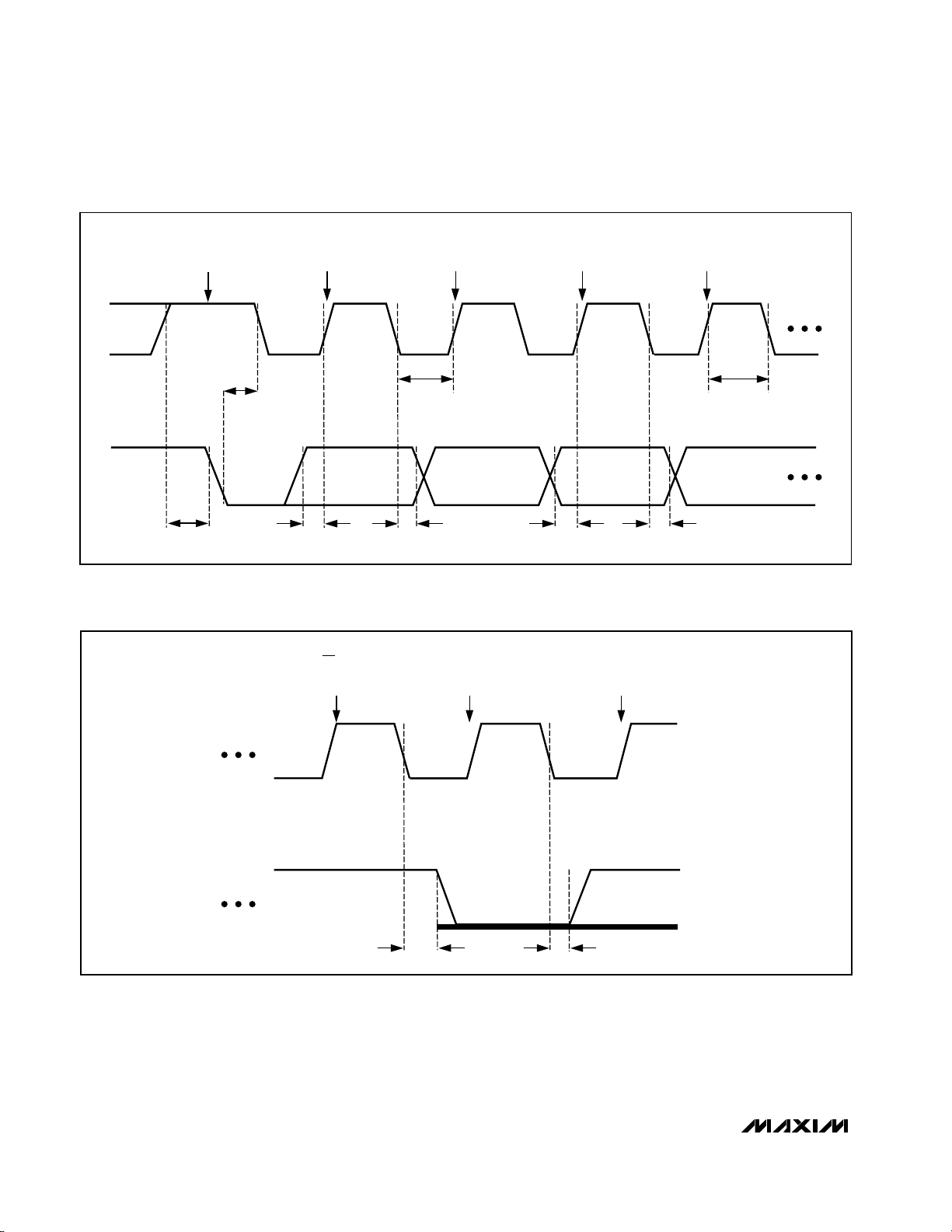
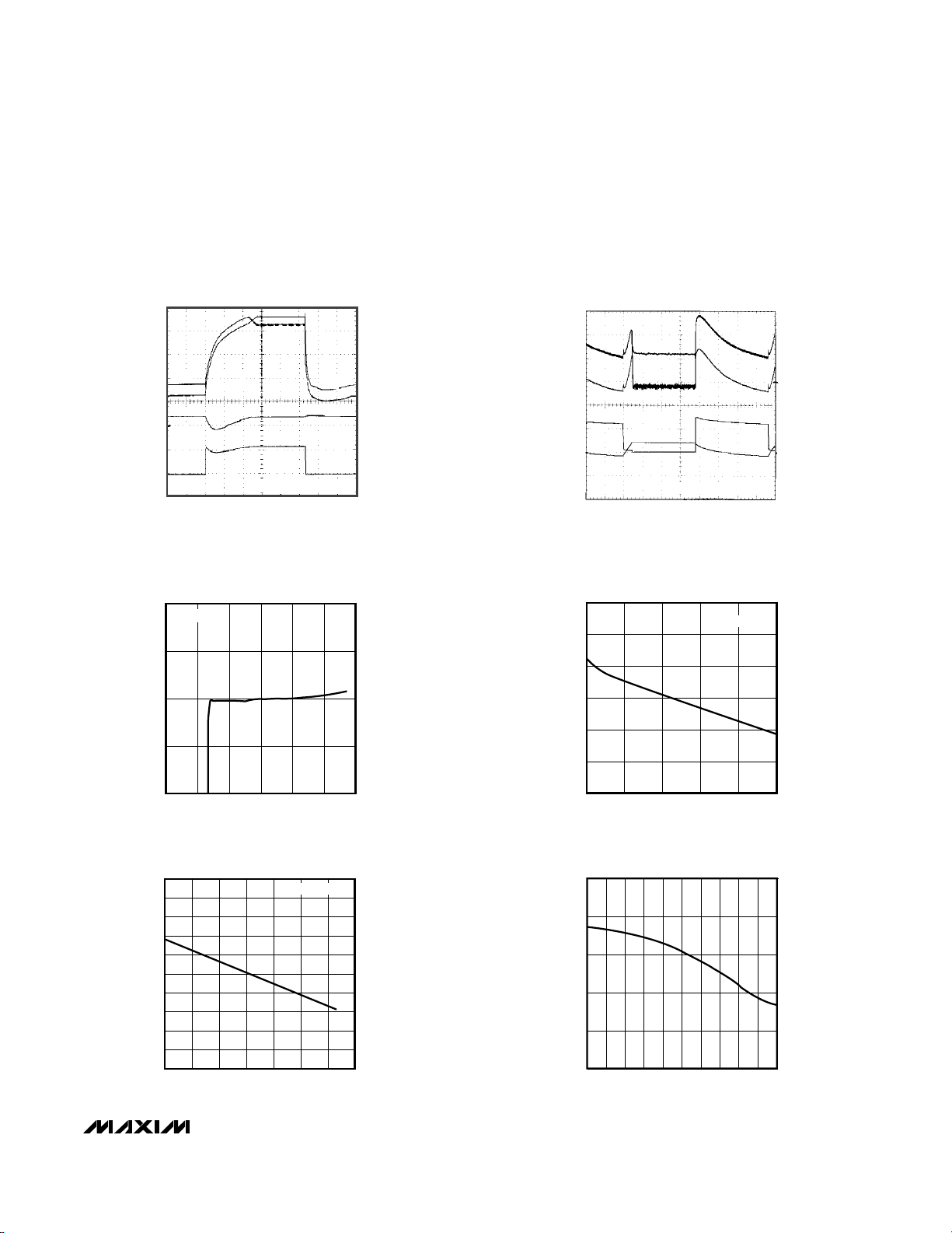
__________________________________________Typical Operating Characteristics
(Circuit of Figure 7, TA = +25°C, unless otherwise noted.)
(VOLTAGE REGULATION WITH CURRENT LIMIT)
10V
5V/div
V
DCIN
ChargingVoltage() = 12,000mV
ChargingCurrent() = 1500mA
CCI
CCV
= 18V
LOAD TRANSIENT
CCV
CCI
CCV
CCI
V
BATT
I
LOAD
AVERAGED MEASUREMENT
500µs/div
CCI
CCV
MAX1667TOC01
200mV/div
1.4V
1A
1A/div
(WITH CHANGE IN REGULATION LOOP)
LOAD TRANSIENT
CCV
CCI
I
LOAD
10V
5V/div
V
= 18V
DCIN
ChargingVoltage() = 12,000mV
ChargingCurrent() = 1500mA
CCI
CCV
V
BATT
AVERAGED MEASUREMENT
1ms/div
MAX1667TOC02
CCV
CCI
50mV/div
2V
1A
500mA/div
VL LINE REGULATION
5.450
NO LOAD
5.425
5.400
VL (V)
5.375
5.350
010155 202530
V
(V)
DCIN
VL vs. TEMPERATURE
5.45
5.44
5.43
5.42
5.41
5.40
VL (V)
5.39
5.38
5.37
5.36
5.35
-40 -20 0 20 40 60 80 100
TEMPERATURE (°C)
V
DCIN
= 20V
MAX1667 TOC03
MAX1667 TOC05
VL LOAD REGULATION
5.50
5.45
5.40
5.35
VL (V)
5.30
5.25
5.20
0105 152025
LOAD CURRENT (mA)
V
LOAD REGULATION
REF
0 0.80.60.2 0.4 1.0 1.2 1.4 1.6 1.8 2.0
LOAD CURRENT (mA)
(V)
V
4.11
4.10
4.09
REF
4.08
4.07
4.06
V
= 20V
DCIN
MAX1667 TOC04
MAX1667 TOC06
MAX1667
Chemistry-Independent,
Level 2 Smart Battery Charger
8 _______________________________________________________________________________________
Typical Operating Characteristics (continued)
(Circuit of Figure 7, TA = +25°C, unless otherwise noted.)
100
0.01
10
1.0
0.1
0.001
0 400 800 1200 1600 2000
OUTPUT V-I CHARACTERISTIC
(SWITCHING REGULATOR)
MAX1667 TOC10
LOAD CURRENT (mA)
DROP IN BATT OUTPUT VOLTAGE (%)
V
DCIN
= 20V
ChargingVoltage() = 17,408mV
ChargingCurrent() = 1920mA
V
REF
= 4.096V
0
5
1
3
4
8
02468101214161820
OUTPUT V-I CHARACTERISTIC
(LINEAR SOURCE)
MAX1667 TOC11
V
IOUT
(V)
I
IOUT
(mA)
2
6
7
V
DCIN
= 20V
ChargingVoltage() = 17,408mV
ChargingCurrent() = 1 to 127mA
4.080
4.100
4.085
4.090
4.095
4.110
-40 4020-20 0 60 80 100
V
REF
vs. TEMPERATURE
MAX1667 TOC07
TEMPERATURE (°C)
V
REF
(V)
4.105
V
DCIN
= 20V
50
70
55
60
65
100
0 20001000 3000 4000
EFFICIENCY vs. LOAD CURRENT
(VOLTAGE REGULATION)
MAX1667 TOC08
LOAD CURRENT (mA)
EFFICIENCY (%)
75
80
85
90
95
A: V
DCIN
= 20V, V
BATT
= 17V
B: V
DCIN
= 16V, V
BATT
= 12.75V
C: V
DCIN
= 20V, V
BATT
= 12.75V
D: V
DCIN
= 16V, V
BATT
= 8.5V
E: V
DCIN
= 20V, V
BATT
= 8.5V
A
B
C
E
D
50
70
55
60
65
100
0862 4 10 12 18
EFFICIENCY vs. BATT VOLTAGE
(CURRENT REGULATION)
MAX1667 TOC09
BATT VOLTAGE (V)
EFFICIENCY (%)
75
80
85
90
95
14 16
A: V
DCIN
= 16V, I
LOAD
= 2A
B: V
DCIN
= 20V, I
LOAD
= 2A
C: V
DCIN
= 20V, I
LOAD
= 600mA
A
B
C
BATT VOLTAGE ERROR (%)
BATT VOLTAGE ERROR
vs. ChargingVoltage() CODE
1.0
0.8
V
= 20V
DCIN
MEASURED AT AVAILABLE
0.6
ChargingVoltage() CODES
0.4
0.2
0
-0.2
-0.4
-0.6
-0.8
-1.0
0 4k6k8k2k 10k 12k 14k 18k16k 20k
ChargingVoltage() CODE
I
LOAD
I
LOAD
= 600mA
= 3mA
MAX1667 TOC12
LOAD CURRENT ERROR
15
10
5
BATT CURRENT ERROR (%)
0
-5
V
=20V
DCIN
V
= 12.75V
BATT
MEASURED AT AVAILABLE
ChargingCurrent() CODES
0 1000 2000 3000500 1500 2500 3500 4000
CODE
MAX1667 TOC13
MAX1667
Chemistry-Independent,
Level 2 Smart Battery Charger
_______________________________________________________________________________________ 9
Pin Description
Linear Current-Source Output1 IOUT
Input Voltage for Powering Charger2 DCIN
Voltage-Regulation-Loop Compensation Point4 CCV
IC Power Supply. 5.4V linear-regulator output from DCIN.3 VL
Current-Range Selector. Connecting SEL to VL sets a 4A full-scale current. Leaving SEL
open sets a 3A full-scale current. Connecting SEL to AGND sets a 1A full-scale current.
6 SEL
Battery Voltage Input and Current-Sense Negative Input8 BATT
Current-Sense Positive Input7 CS
Current-Regulation-Loop Compensation Point5 CCI
+4.096V Reference Voltage Output or External Reference Input9 REF
Open-Drain Interrupt Output11
INT
Analog Ground10 AGND
Thermistor Sense Voltage Input12 THM
Serial Data (need external pull-up resistor)14 SDA
Power Ground16 PGND
Voltage DAC Output Filtering Point15 DACV
Serial Clock (need external pull-up resistor)13 SCL
High-Side Power MOSFET Driver Output18 DHI
Power Connection for the High-Side Power MOSFET Driver20 BST
Power Connection for the High-Side Power MOSFET Driver19 LX
Low-Side Power MOSFET Driver Output17 DLO
FUNCTIONPIN NAME
MAX1667
Chemistry-Independent,
Level 2 Smart Battery Charger
Smart Battery Charging System
A smart battery charging system, at a minimum, consists of a smart battery and smart battery charger compatible with the Smart Battery System specifications
using Intel’s system management bus (SMBus).
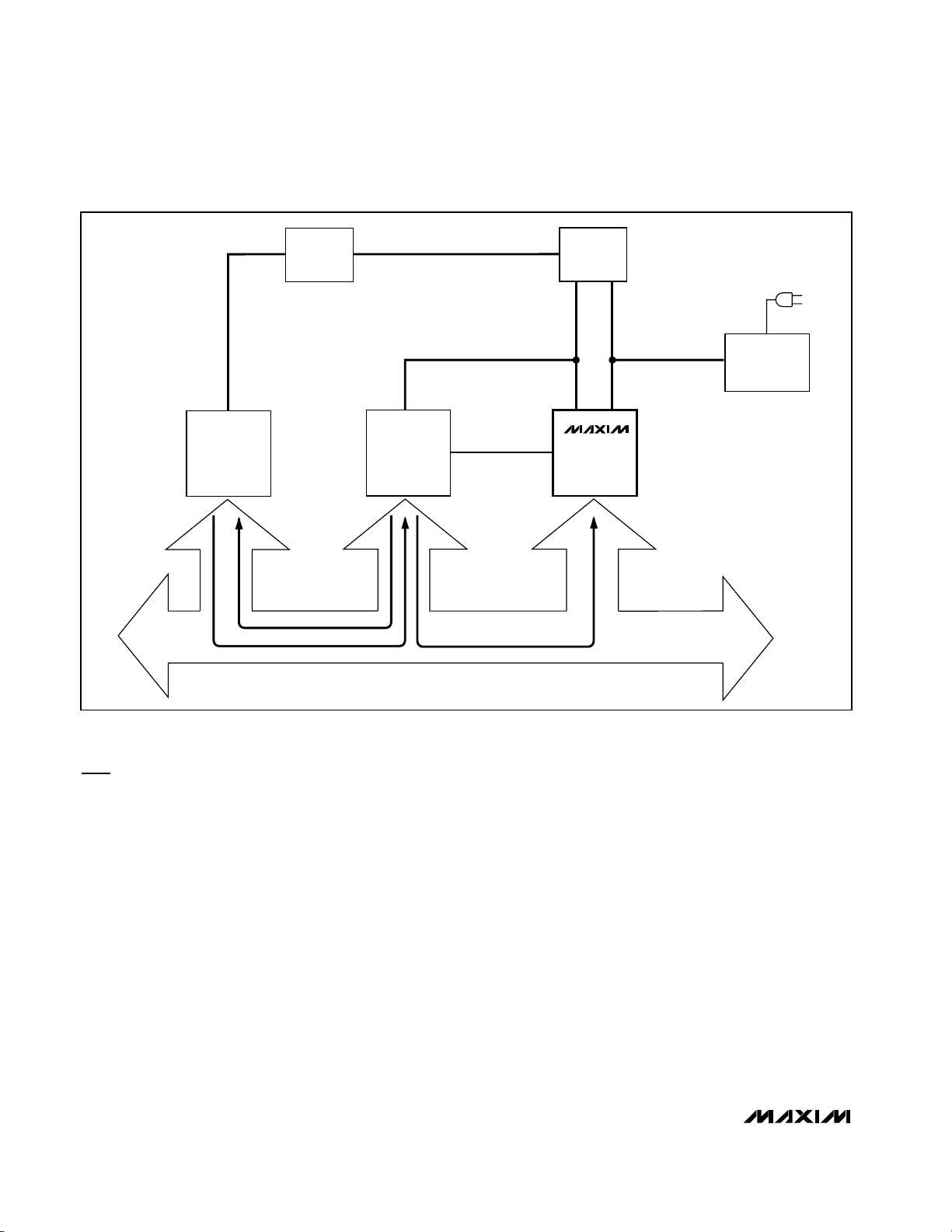
Smart Battery System Block Diagrams
A system may use one or more smart batteries. The
block diagram of a smart battery charging system
shown in Figure 3 depicts a single battery system. This
is typically found in notebook computers, video cameras, cellular phones, and other portable electronic
equipment.
Another possibility is a system that uses two or more
smart batteries. A block diagram for a system featuring
multiple batteries is shown in Figure 4. The smart battery selector is used to connect batteries to either the
smart battery charger or the system, or to disconnect
them, as appropriate. For a standard smart battery, the
following connections must be made: power (the bat-
tery’s positive and negative terminals), SMBus (clock
and data), and safety signal (resistance, typically temperature dependent). Additionally, the system host
must be able to query any battery in the system so it
can display the state of all batteries present in the system.
Figure 4 shows a two-battery system where Battery 2 is
being charged while Battery 1 is powering the system.
This configuration may be used to “condition” Battery
1, allowing it to be fully discharged prior to recharge.
Smart Battery Charger Types
Two types of smart battery chargers are defined: Level
2 and Level 3. All smart battery chargers communicate
with the smart battery using the SMBus; the two types
differ in their SMBus communication mode and in
whether they modify the charging algorithm of the
smart battery as shown in Table 1. Level 3 smart battery chargers are supersets of Level 2 chargers and as
such support all Level 2 charger commands.
SYSTEM
POWER
CONTROL
AC-DC
CONVERTER
(UNREGULATED)
AC
SYSTEM
POWER
SUPPLY
DC (UNREGULATED) / V
BATTERY
SAFETY
SIGNAL
V
BATTERY
DC (UNREGULATED)
V
CC
+12V, -12V
SYSTEM HOST
(SMBus HOST)
SMART BATTERY
CRITICAL EVENTS
CRITICAL EVENTS
CHARGING VOLTAGE/CURRENT
REQUESTS
BATTERY DATA/STATUS REQUESTS
SMART BATTERY
CHARGER
SMBus
MAX1667
Figure 3. Typical Single Smart Battery System
10 ______________________________________________________________________________________

MAX1667
Chemistry-Independent,
Level 2 Smart Battery Charger
______________________________________________________________________________________ 11
Level 2 Smart Battery Charger
The Level 2 or “smart-battery-controlled” smart battery
charger interprets the smart battery’s critical warning
messages, and operates as an SMBus slave device
that responds to ChargingVoltage() and ChargingCurrent() messages sent to it by a smart battery. The
charger is obliged to adjust its output characteristics in
direct response to the messages it receives from the
battery. In Level 2 charging, the smart battery is completely responsible for initiating communication and for
providing the charging algorithm to the charger. The
smart battery is in the best position to tell the smart battery charger how it needs to be charged. The charging
algorithm in the battery may request a static charge
condition or may choose to periodically adjust the
smart battery charger’s output to meet its present
needs. A Level 2 smart battery charger is truly chemistry independent, and since it is defined as an SMBus
slave device only, it is relatively inexpensive and easy
to implement.
Table 1. Charger Type by SMBus Mode
and Charge Algorithm Source
Level 3Level 3Slave/Master
Level 3Level 2
Modified from BatteryBattery
Slave Only
SMBus MODE
CHARGE ALGORITHM SOURCE
Note: Level 1 smart battery chargers are defined in the ver-
sion 0.95a specification. While they can correctly interpret
smart battery end-of-charge messages minimizing overcharge, they do not provide truly chemistry-independent
charging. They are no longer defined by the Smart Battery
Charger specification and are explicitly not compliant with this
and subsequent Smart Battery Charger specifications.
AC-DC
CONVERTER
(UNREGULATED)
AC
DC (UNREGULATED) / V
BATTERY
NOTE: SB 1 POWERING SYSTEM
SB 2 CHARGING
V
CC
+12V, -12V
SYSTEM HOST
(SMBus HOST)
SMART BATTERY
SELECTOR
SMBus
SMBus
SMBus
SAFETY SIGNAL
V
CHARGE
V
BATT
SAFETY
SIGNAL
V
BATT
SAFETY
SIGNAL
SMART BATTERY 1
SMART BATTERY 2
CRITICAL EVENTS
BATTERY DATA/STATUS REQUESTS
SMART BATTERY
CHARGER
SMBus
MAX1667
SYSTEM
POWER
SUPPLY
Figure 4. Typical Multiple Smart Battery System

MAX1667
Chemistry-Independent,
Level 2 Smart Battery Charger
12 ______________________________________________________________________________________
_______________Detailed Description
Output Characteristics
The MAX1667 contains both a voltage-regulation loop
and a current-regulation loop. Both loops operate independently of each other. The voltage-regulation loop
monitors BATT to ensure that its voltage never exceeds
the voltage set point (V0). The current-regulation loop
monitors current delivered to BATT to ensure that it
never exceeds the current-limit set point (I0). The current-regulation loop is in control as long as BATT voltage is below V0. When BATT voltage reaches V0, the
current loop no longer regulates, and the voltage-regulation loop takes over. Figure 5 shows the V-I characteristic at the BATT pin.
Setting V0 and I0
Set the MAX1667’s voltage and current-limit set points
via the Intel SMBus 2-wire serial interface. The
MAX1667’s logic interprets the serial-data stream from
the SMBus interface to set internal digital-to-analog converters (DACs) appropriately. The power-on-reset value
for V0 and I0 is 18.4V and 7mA, respectively. See
Digital
Section
for more information.
_____________________Analog Section
The MAX1667 analog section consists of a currentmode pulse-width-modulated (PWM) controller and two
transconductance error amplifiers—one for regulating
current and the other for regulating voltage. The device
uses DACs to set the current and voltage level, which
are controlled via the SMBus interface. Since separate
amplifiers are used for voltage and current control, both
control loops can be compensated separately for optimum stability and response in each state.
Whether the MAX1667 is controlling the voltage or current at any time depends on the battery’s state. If the
battery has been discharged, the MAX1667’s output
reaches the current-regulation limit before the voltage
limit, causing the system to regulate current. As the battery charges, the voltage rises until the voltage limit is
reached, and the charger switches to regulating voltage.
The transition from current to voltage regulation is done
by the charger and need not be controlled by the host.
Figure 6 shows the MAX1667 block diagram.
Voltage Control
The internal GMV amplifier controls the MAX1667’s output voltage. The voltage at the amplifier’s noninverting
input is set by an 11-bit DAC, which is controlled by a
ChargingVoltage() command on the SMBus (see
Digital
Section
for more information). The battery voltage is fed
to the GMV amplifier through a 5:1 resistive voltage
divider. The set voltage ranges between 0 and 18.416V
with 16mV resolution. This allows up to four Li+ cells in
series to be charged.
The GMV amplifier’s output is connected to the CCV
pin, which compensates the voltage-regulation loop.
Typically, a series-resistor/capacitor combination can
be used to form a pole-zero doublet. The pole introduced rolls off the gain starting at low frequencies. The
zero of the doublet provides sufficient AC gain at midfrequencies. The output capacitor then rolls off the midfrequency gain to below 1 to guarantee stability before
encountering the zero introduced by the output capacitor’s equivalent series resistance (ESR). The GMV
amplifier’s output is internally clamped to between onefourth and three-fourths of the voltage at REF.
Current Control
An internal 7mA linear current source is used in conjunction with the PWM regulator to set the battery
charge current. When the current is set to 0, the voltage
regulator is on but no current is available. A current setting between 1mA and 127mA turns on the linear current source, providing a maximum of 7mA for trickle
charging. For current settings above 127mA, the linear
current source is disabled and the charging current is
provided by the switching regulator set by the 5-bit current-control DAC.
The GMI amplifier’s noninverting input is driven by a 4:1
resistive voltage divider, which is driven by the 5-bit
DAC. With the internal 4.096V reference, this input is
approximately 1.0V at full scale, and the resolution is
31mV. The current-sense amplifier drives the inverting
input to the GMI amplifier. It measures the voltage
Figure 5. Output V-I Characteristic
BATT
VOLTAGE
V0
V0 = VOLTAGE SET POINT
I0 = CURRENT-LIMIT SET POINT
AVERAGE CURRENT
THROUGH THE RESISTOR
I0
BETWEEN CS AND BATT

MAX1667
Chemistry-Independent,
Level 2 Smart Battery Charger
______________________________________________________________________________________ 13
Figure 6. Functional Diagram
REF
THM
AGND
CS
BATT
FROM LOGIC
BLOCK
FROM LOGIC BLOCK
BATT
FROM LOGIC BLOCK
10k 10k
100k
CURRENT-SENSE
LEVEL SHIFT AND
GAIN OF 5.5
5
5-BIT DAC
AGND
4R
R
AGND
30k 3k
REF
11
10k
3R
R
TO LOGIC BLOCK
TO LOGIC BLOCK
REF
11-BIT DAC
10k
500Ω
VOLTAGE_INREG
CURRENT_INREG
THERMISTOR_OR
THERMISTOR_COLD
THERMISTOR_HOT
THERMISTOR_UR
CCI
GMI
CLAMP
GMV
CCV
DACV
LOGIC
BLOCK
CCV_LOW
3/8 REF = ZERO CURRENT
NOTE: APPROX. REF/4 + V
TO 3/4 REF + V
MIN
THRESH
NOTE:
REF/4 TO 3/4 REF
CLAMP
TO REF
(MAX)
AGND
THERM_SHUT
SEL
SCL
SDA
INT
AC_PRESENT
THRESH
FROM LOGIC
BLOCK
7mA
THERMAL
SHUTDOWN
DCIN
5.4V LINEAR
REGULATOR
R
AGND
LEVEL
SHIFT
SUMMING
COMPARATOR
BLOCK
DCIN
MAX1667
IOUT
VL
INTERNAL
4.096V
REFERENCE
AGND
CCV
3R
REF
BST
DRIVER
LX
VL
DRIVER
PGND
REF
DHI
DLO
AGND
TO LOGIC BLOCK
POWER_FAIL
DCIN/4.5

MAX1667
Chemistry-Independent,
Level 2 Smart Battery Charger
14 ______________________________________________________________________________________
across the current-sense resistor (R
SEN
) (which is
between the CS and BATT pins), amplifies it by approximately 5.45, and level shifts it to ground. The full-scale
current is approximately 0.16V/R
SEN
, and the resolution
is 5mV/R
SEN
.
The current-regulation loop is compensated by adding a
capacitor to the CCI pin. This capacitor sets the currentfeedback loop’s dominant pole. The GMI amplifier’s output is clamped to between approximately one-fourth
and three-fourths of the REF voltage. While the current is
in regulation, the CCV voltage is clamped to within
80mV of the CCI voltage. This prevents the battery voltage from overshooting when the DAC voltage setting is
updated. The converse is true when the voltage is in
regulation and the current is not at the current DAC setting. Since the linear range of CCI or CCV is about 1.5V
to 3.5V (about 2V), the 80mV clamp results in a relatively
negligible overshoot when the loop switches from voltage to current regulation or vice versa.
PWM Controller
The battery voltage or current is controlled by the current-mode, PWM, DC-DC converter controller. This controller drives two external N-channel MOSFETs, which
switch the voltage from the input source. This switched
voltage feeds an inductor, which filters the switched rectangular wave. The controller sets the pulse width of the
switched voltage so that it supplies the desired voltage
or current to the battery.
The heart of the PWM controller is the multi-input comparator. This comparator sums three input signals to
determine the pulse width of the switched signal, setting the battery voltage or current. The three signals are
the current-sense amplifier’s output, the GMV or GMI
error amplifier’s output, and a slope-compensation signal, which ensures that the controller’s internal currentcontrol loop is stable.
The PWM comparator compares the current-sense
amplifier’s output to the lower output voltage of either
the GMV or the GMI amplifier (the error voltage). This
current-mode feedback corrects the duty ratio of the
switched voltage, regulating the peak battery current
and keeping it proportional to the error voltage. Since
the average battery current is nearly the same as the
peak current, the controller acts as a transconductance
amplifier, reducing the effect of the inductor on the output filter LC formed by the output inductor and the battery’s parasitic capacitance. This makes stabilizing the
circuit easy, since the output filter changes from a complex second-order RLC to a first-order RC. To preserve
the inner current-control loop’s stability, slope compensation is also fed into the comparator. This damps out
perturbations in the pulse width at duty ratios greater
than 50%.
At heavy loads, the PWM controller switches at a fixed
frequency and modulates the duty cycle to control the
battery voltage or current. At light loads, the DC current
through the inductor is not sufficient to prevent the current from going negative through the synchronous rectifier (Figure 7, M2). The controller monitors the current
through the sense resistor R
SEN
; when it drops to zero,
the synchronous rectifier turns off to prevent negative
current flow.
MOSFET Drivers
The MAX1667 drives external N-channel MOSFETs to
regulate battery voltage or current. Since the high-side
N-channel MOSFET’s gate must be driven to a voltage
higher than the input source voltage, a charge pump is
used to generate such a voltage. The capacitor C7
(Figure 7) charges to approximately 5V through D2
when the synchronous rectifier turns on. Since one side
of C7 is connected to the LX pin (the source of M1), the
high-side driver (DHI) can drive the gate up to the voltage at BST (which is greater than the input voltage)
when the high-side MOSFET turns on.
The synchronous rectifier may not be completely
replaced by a diode because the BST capacitor
charges while the synchronous rectifier is turned on.
Without the synchronous rectifier, the BST capacitor
may not fully charge, leaving the high-side MOSFET
with insufficient gate drive to turn on. Use a small MOSFET, such as a 2N7002, to guarantee that the BST
capacitor is allowed to charge. In this case, most of the
current at high currents is carried by the Schottky diode
and not by the synchronous rectifier.
Internal Regulator and Reference
The MAX1667 uses an internal low-dropout linear regulator to create a 5.4V power supply (VL), which powers its
internal circuitry. VL can supply up to 20mA, less than
10mA powers the internal circuitry, and the remaining
current can power the external circuitry. The current
used to drive the MOSFETs comes from this supply,
which must be considered when calculating how much
power can be drawn. To estimate the current required to
drive the MOSFETs, multiply the total gate charge of
each MOSFET by the switching frequency (typically
250kHz). To ensure VL stability, bypass the VL pin with a
1µF or greater capacitor.
The MAX1667 has an internal, accurate 4.096V reference voltage. This guarantees a voltage-setting accuracy of ±1% max. Bypass the reference with a 1µF or
greater capacitor.

MAX1667
Chemistry-Independent,
Level 2 Smart Battery Charger
______________________________________________________________________________________ 15
Figure 7. Typical Application Circuit
AGND
D2
C9
R5
R6
C6
M1
M2
D1
D4*
D3
DC SOURCE
C1
L1
D5
R1
C7
C11
REF
R3
C4
C10
THM
CCI
IOUT
C5
(NOTE 2)
10
1
2
6
3
20
18
19
17
16
7
8
13
14
11
9
12
5
4
15
= HIGH-CURRENT TRACES (8A MAX)
NOTE 1: C6, M2, D1, AND C1 GROUNDS MUST CONNECT TO
THE SAME RECTANGULAR PAD ON THE LAYOUT.
NOTE 2: C5 AND C11 MUST BE PLACED WITHIN 0.5cm OF THE
MAX1667, WITH TRACES NO LONGER THAN 1cm
CONNECTING VL AND PGND.
*OPTIONAL (SEE
NEGATIVE INPUT VOLTAGE PROTECTION
SECTION).
SEE TABLES 2a AND 2b FOR COMPONENT SELECTION AND MANUFACTURERS.
C8
C2
R2
C3
R4
DCIN
MAX1667
SEL
VL
BST
CCV
DACV
LX
DLO
PGND
CS
DHI
(NOTE 1)
SMART BATTERY
STANDARD CONNECTOR
-TD C+
BATT
SCL
SDA
INT
HOST & LOAD
SMBCLOCK
V+
SMBDATA
KINT-
GND
7.5V–28V
MAX1667
Chemistry-Independent,
Level 2 Smart Battery Charger
16 ______________________________________________________________________________________
Table 2a. Component Selection
_____________________Digital Section
SMBus Interface
The MAX1667 uses serial data to control its operation. The
serial interface complies with the SMBus specification (see
System Management Bus Specification
, from the SBS
forum at www.sbs-Forum.org or from Intel Architecture
Labs: 800-253-3696). Charger functionality complies with
the Duracell/Intel Smart Charger Specification for a Level 2
charger.
The MAX1667 uses the SMBus Read-Word and WriteWord protocols to communicate with the battery it is
charging, as well as with any host system that monitors
the battery to charger communications. The MAX1667
acts only as a slave device and never initiates communication on the bus; it receives commands and responds
to queries for status information. Figures 8a and 8b show
the SMBus Write-Word and Read-Word protocols.
Each communication with the MAX1667 begins with the
master issuing a START condition, which is a high-tolow transition on SDA while SCL is high (Figure 1).
DESIGNATION MANUFACTURER
M2
Low-Side MOSFET
C8
R1
Sense Resistor
40mΩ ±1%, 1W
2N7002 equivalent
D2, D3 Central
Sprague 594D686X0025R2T
C1
Output Capacitor
TPSE686M020R0150
68µF, 20V, low ESR
IRF7805
M1
High-Side MOSFET
IR IRF7603 IRF7201
R5, R6 33Ω ±5%, 1/16W
R3 10kΩ ±1%, 1/16W
R2, R4 10kΩ ±5%, 1/16W
4A1A 3A
C4, C5, C9, C10 1µF
C2, C7, C11
C3 47nF
0.1µF
C6
Input Capacitor
Sprague 594D226X0035R2T
TPSE226M035R0200
2 x 22µF, 35V, low ESR
D1, D4, D5
Schottky Diodes
Central CMSH3-40 CMSH5-40
MBRS130LT3 MBRS340T3
1N5819 equivalent 1N5821 equivalent
MBRS340T3
1N5821 equivalent
AVX
AVX
Motorola
Motorola MMBF1170LT1
L1
Inductor
33µH, 1A ISAT 33µH, 3A ISAT, 30V 33µH, 4A ISAT, 30V
Sumida CDH74-330 CDRH127-330 CDRH127-270
Coiltronics UP1B-330 UP3B-330
Coilcraft DS3316P-333
FDS6680Fairchild FDN359A FDS4410
Motorola MTSF3N03HD MMDF3N03HD
IRC LR251201R040F
Dale WSL-2512/0.04W/±1%
22nF
Schottky diode, 50mA IDC, 30V, CMPSH-3
NIEC EC31 NSQ03A04 CMSH5-40

MAX1667
Chemistry-Independent,
Level 2 Smart Battery Charger
______________________________________________________________________________________ 17
When the master has finished communicating with the
slave, the master issues a STOP condition, which is a
low-to-high transition on SDA while SCL is high. The
bus is then free for another transmission. Figures 1 and
2 show timing diagrams for signals on the SMBus interface. The address byte, control byte, and data bytes
are transmitted between the START and STOP conditions. Data is transmitted in 8-bit words, and after each
byte either the slave or the master issues an acknowledgment (Figure 2); therefore, nine clock cycles are
required to transfer each byte. The SDA state is allowed
to change only while SCL is low, except for the START
and STOP conditions.
The MAX1667 7-bit address is preset to 0b0001001.
The eighth bit indicates a Write-Word (W = 0) or a
Read-Word (R = 1) command. This can also be denoted by the hexadecimal number 0x12 for a Write-Word
command or a 0x13 for a Read-Word command.
The following commands use the Write-Word protocol
(Figure 8a): ChargerMode(), ChargingVoltage(),
ChargingCurrent(), and AlarmWarning(). The
ChargerStatus command uses the Read-Word protocol
(Figure 8b).
ChargerMode()
The ChargerMode() command uses Write-Word protocol
(Figure 8a). The command code for ChargerMode() is
0x12 (0b00010010). Table 3 describes the functions of
the 16 data bits (D0–D15). Bit 0 refers to the D0 bit in the
Write-Word protocol.
Whenever the BATTERY_PRESENT status bit (bit 14) of
ChargerStatus() is clear, the HOT_STOP bit is set,
regardless of any previous ChargerMode() command.
To charge a battery that has a thermistor impedance
in the HOT range (i.e., THERMISTOR_HOT = 1 and
THERMISTOR_UR = 0), the host must use the
ChargerMode() command to clear HOT_STOP after the
battery is inserted. The HOT_STOP bit returns to its
default power-up condition (‘1’) whenever the battery is
removed.
ChargingVoltage()
The ChargingVoltage() command uses Write-Word protocol (Figure 8a). The command code for ChargingVoltage()
is 0x15 (0b00010101). The 16-bit binary number formed
by D15–D0 represents the voltage set point (V0) in millivolts; however, since the MAX1667 has only 16mV of resolution in setting V0, the D0, D1, D2, and D3 bits are
ignored.
The maximum voltage delivered by the MAX1667 is
18.416V, corresponding to a ChargingVoltage() value of
0x47F0. This is also the floating voltage set by the
power-on reset (POR). ChargingVoltage() values above
0x47F0 deliver the floating voltage and set the VOLTAGE_OR status bit. Any time the BATTERY_PRESENT
status bit is clear, the ChargingVoltage() register
returns to its POR state.
Figure 9 shows the mapping between V0 (the voltageregulation-loop set point) and the ChargingVoltage()
data.
ChargingCurrent()
The ChargingCurrent() command uses Write-Word protocol (Figure 8a). The command code for ChargingCurrent()
is 0x14 (0b00010100). The 16-bit binary number formed
by D15–D0 represents the current-limit set point (I0) in
milliamps (Table 4). Connecting SEL to AGND selects a
0.896A maximum setting for I0. Leaving SEL open selects
a 2.944A maximum setting for I0. Connecting SEL to VL
selects a 3.968A maximum setting for I0.
Two sources of current in the MAX1667 charge the battery: a linear current source begins from IOUT, and a
switching regulator controls the current flowing through
the current-sense resistor (R1). IOUT provides a tricklecharge current to compensate for battery self-discharge,
while the switching regulator provides large currents for
fast charging.
IOUT sources 7mA, while the switching regulator
sources from 128mA to 3968mA with a 5-bit resolution
(LSB = 5.12mV / RSENSE = 128mA with a 40mΩ sense
resistor). In Table 4, DA4–DA0 denotes the bits in the
current DAC code. Table 5 shows the relationship
between the value programmed with the ChargingCurrent() command and IOUT source current. The
CCV_LOW comparator checks to see if the output volt-
Table 2b. Component Suppliers
847-639-1469847-639-6400Coilcraft
516-435-1824516-435-1110
803-626-3123803-946-0690AVX
Central Semiconductor
561-241-9339561-241-7876Coiltronics
FAXPHONEMANUFACTURER
512-992-3377512-992-7900IRC
310-322-3332310-322-3331
605-665-1627605-668-4131Dale
IR
805-867-2698805-867-2555NIEC
603-224-1430603-224-1961
408-970-3950408-988-8000Siliconix
Sprague
847-956-0702847-956-0666Sumida
516-864-7630516-543-7100Zetex

MAX1667
Chemistry-Independent,
Level 2 Smart Battery Charger
18 ______________________________________________________________________________________
age is too high by comparing CCV to REF/4. If
CCV_LOW = 1 (when CCV < REF/4), IOUT shuts off.
This prevents the output voltage from exceeding the
voltage set point specified by the ChargingVoltage()
register. VOLTAGE_NOTREG = 1 whenever the internal
clamp pulls down on CCV. (The internal clamp pulls
down on CCV to keep its voltage close to CCI’s voltage.)
With the switching regulator on, the current through R1
(Figure 7) is regulated by sensing the average voltage
between CS and BATT. Figure 10 shows the relationship between the ChargingCurrent() data and the average voltage between CS and BATT.
When the switching regulator is off, DHI is forced to
LX and DLO is forced to ground. This prevents current
from flowing through inductor L1. Table 6 shows the
relationship between the ChargingCurrent() register
value and the switching regulator current DAC code
(DA4–DA0).
To ensure that the actual output current matches the
data value programmed with the ChargingCurrent()
command, R1 should be as close as possible to 40mΩ.
The SEL pin setting affects the full-scale current but not
the step size. ChargingCurrent() values above the full-
scale setting set the CURRENT_OR status bit. Note that
whenever any current DAC bits are set, the linear-current source is turned off.
The power-on reset value for the ChargingCurrent() register is 0x0007. Any time the BATTERY_PRESENT status
bit is clear (battery removed), the ChargingCurrent()
register returns to its power-on reset state. This ensures
that upon insertion of a battery, the initial charging current is 7mA.
AlarmWarning()
The AlarmWarning() command uses Write-Word protocol
(Figure 8a). The command code for AlarmWarning() is
0x16 (0b00010110). The AlarmWarning() command sets
the ALARM_INHIBITED status bit. The MAX1667 responds
to the following alarms: OVER_CHARGED_ALARM (D15),
TERMINATE_CHARGE_ALARM (D14), and OVER_TEMP_
ALARM (D12). Table 7 summarizes the AlarmWarning()
command’s function. The ALARM_INHIBITED status bit
remains set until BATTERY_PRESENT = 0 (battery
removed), a ChargerMode() command is written with the
POR_RESET bit set, or a new ChargingVoltage() or
ChargingCurrent() is written.
—7–9N/A
05
—4N/A
BATTERY_PRESENT_MASK
—
11–15
(MSB)
N/A Not implemented. Write 1 into this bit.
110HOT_STOP
Not implemented. Write 1 into this bit.
0 = Interrupt on either edge of the BATTERY_PRESENT status bit.
1 = Do not interrupt because of a BATTERY_PRESENT bit change.
Not implemented. Write 1 into this bit.
0 = The THERMISTOR_HOT status bit does not turn the charger off.
1 = THERMISTOR_HOT turns the charger off.
0 = No change in any non-ChargerMode() settings.
1 = Change the voltage and current settings to 0xFFFF and 0x0007
respectively; clear the THERMISTOR_HOT and ALARM_INHIBITED bits.
Not implemented. Write 0 into this bit.
0 = Allow normal operation; clear the CHG_INHIBITED status bit.
1 = Turn the charger off; set the CHG_INHIBITED status bit.
Not implemented. Write 0 into this bit.
FUNCTION
—2POR_RESET
—1
0
0
(LSB)
INHIBIT_CHARGE
ENABLE_POLLING
—3RESET_TO_ZERO
POR
VALUE**
BIT
POSITION*
BIT NAME
Table 3. ChargerMode() Bit Functions
16POWER_FAIL_MASK
0 = Interrupt on either edge of the POWER_FAIL status bit.
1 = Do not interrupt because of a POWER_FAIL bit change.
*
Bit position in the D15–D0 data. **Power-on reset value.
N/A = Not applicable

MAX1667
Chemistry-Independent,
Level 2 Smart Battery Charger
______________________________________________________________________________________ 19
ChargerStatus()
The ChargerStatus() command uses Read-Word protocol (Figure 8b). The command code for ChargerStatus()
is 0x13 (0b00010011). The ChargerStatus() command
returns information about thermistor impedance and the
MAX1667’s internal state. The Read-Word protocol
returns D15–D0. Table 8 describes the meaning of the
individual bits. The latched bits, THERMISTOR_HOT
and ALARM_INHIBITED, are cleared whenever BATTERY_PRESENT = 0 or ChargerMode() is written with
POR_RESET = 1.
Interrupts and the
Alert-Response Address
An interrupt is triggered (INT goes low) whenever power
is applied to DCIN, the BATTERY_PRESENT bit changes,
or the POWER_FAIL bit changes. BATTERY_PRESENT
and POWER_FAIL have interrupt masks that can be set
or cleared via the ChargerMode() command. INT stays
low until the interrupt is cleared. There are two methods
for clearing the interrupt: issuing a ChargerStatus() command, and using a modified Receive Byte protocol with a
0x19 (0b0011001) Alert-Response address. The
MAX1667 responds to the Alert-Response address with
its address (0x13) left justified as the most significant bits
of the returned byte.
__________Applications Information
Negative Input Voltage Protection
In most portable equipment, the DC power to charge
batteries enters through a two-conductor cylindrical
power jack. It is easy for the end user to add an
adapter to switch the DC power’s polarity. Polarized
capacitor C6 would be destroyed if a negative voltage
were applied. Diode D4 in Figure 7 prevents this from
happening.
Figure 8. SMBus a) Write-Word and b) Read-Word Protocols
0MSB LSB
1b7 bits
W
SLAVE
ADDRESS
S
1b
ACK S
MSB LSB
1b8 bits
ACK
COMMAND
BYTE
1b
ACK
1MSB LSB
1b7 bits
R
SLAVE
ADDRESS
MSB LSB
1b8 bits
ACK
LOW
DATA
BYTE
P
MSB LSB
1b8 bits
NACK
HIGH
DATA
BYTE
Preset to
0b0001001
D7 D0 D15 D8
ChargerMode() = 0x12
ChargingCurrent() = 0x14
ChargerVoltage() = 0x15
AlarmWarning() = 0x16
Preset to
0b0001001
Preset to
0b0001001
D7 D0 D15 D8
ChargerStatus() =
0x13
1b
ACK S
MSB LSB
1b8 bits
ACK
COMMAND
BYTE
0MSB LSB
1b7 bits
W
SLAVE
ADDRESS
S
MSB LSB
1b7 bits
ACK
LOW
DATA
BYTE
P
MSB LSB
1b8 bits
ACK
HIGH
DATA
BYTE
a) Write-Word Format
b) Read-Word Format
Legend:
S = Start Condition or Repeated Start Condition P = Stop Condition
ACK = Acknowledge (logic low) NACK = NOT Acknowledge (logic high)
W = Write Bit (logic low) R = Read Bit (logic high)
MASTER TO SLAVE
SLAVE TO MASTER

MAX1667
Chemistry-Independent,
Level 2 Smart Battery Charger
20 ______________________________________________________________________________________
Figure 9. ChargingVoltage() Data to Voltage Mapping
18.416V
16.368V
V
REF
= 4.096V
DCIN > 20V
0V
0b000000000000xxxx
0x000x
0x20Dx 0x47Fx
0b001000001101xxxx
0b010010100000xxxx
0x313x
0b001100010011xxxx
0xFFFx
0b111111111111xxxx
0x106x
0b000100000110xxxx
4.192V
12.592V
ChargingVoltage() D15–D0 DATA
VOLTAGE SET POINT (V0)
8.400V
Figure 10. Average Voltage Between CS and BATT vs. Code
Figure 11. Typical Thermistor Characteristics
1000
100
10
RESISTANCE (kΩ)
1
0.1
-40
-50 -30 -20 -10 0 10 20 30 40 50 60 70 80 90 100 110
TEMPERATURE (°C)
160 SEL = VL
115
AVERAGE CS-BATT VOLTAGE
IN CURRENT REGULATION (mV)
35
5
0x0080
A:
B:
C:
0x0380 0x0B80 0x0F80 0xFFFF
(128) (896)
0b00001
0b00111 0b10111 0b11111
A: ChargingCurrent( ) CODE (D15–D0)
B: EQUIVALENT DECIMAL CODE
C: CURRENT DAC CODE (DA4–DA0)
(2944) (3968) (65535)
SEL = OPEN
SEL = GND

MAX1667
Chemistry-Independent,
Level 2 Smart Battery Charger
______________________________________________________________________________________ 21
If reverse-polarity protection for the DC input power is
not necessary, diode D4 can be omitted. This eliminates
the power lost due to the voltage drop on diode D4.
Thermistor Characterization
Figure 11 represents the expected electrical behavior
of a 103ETB-type thermistor (nominally 10kΩ at +25°C
±5% or better) to be used with the MAX1667. The
graph is typical of the suggested thermistor’s characteristics.
THERMISTOR_OR bit is set only when the thermistor
value is > 100kΩ. This indicates that the thermistor is
open.
THERMISTOR_COLD bit is set only when the thermistor
value is > 30kΩ. The thermistor indicates a cold battery.
THERMISTOR_HOT bit is set only when the thermistor
value is < 3kΩ.
THERMISTOR_UR bit is set only when the thermistor
value is < 500Ω.
Multiple bits may be set depending on the values of the
thermistor (e.g., a 450Ω thermistor will cause both the
THERMISTOR_HOT
and
the THERMISTOR_UR bits to
be set). The thermistor may be replaced by fixed-value
resistors in battery packs that do not require the thermistor as a secondary fail-safe indicator. In this case, it
is the responsibility of the battery pack to manipulate
the resistance to obtain correct charger behavior.
Table 4. ChargingCurrent() Bit Functions
2048
DA4
1024
DA3
512
DA2
256
DA1
128
DA0
D15 D14 D13 D12 D11 D10 D9 D8 D7 D6 D5 D4 D3 D2 D1 D0
WEIGHT IN mA
(R
SENSE
= 40mΩ)
FUNCTION
BIT POSITION
3968*
FS* IOUT**
7**
x
0x0010–0xFFFF
0x0010–0xFFFF
0x0010–0xFFFF
0x0010–0xFFFF
0x0000–0x000F
ChargingVoltage()
0x0000
0x0001–0x0007
0x0001–0x0007
0x0008–0x007F
0x0001–0x0007
000
x
ChargingCurrent()
x
1
0
0
1
x
CCV_LOW
x
0
x
x
1
x
VOLTAGE_
NOTREG
0
0
7
7
7
0
000
000
I
OUT
OUTPUT
CURRENT (mA)
0x0010–0xFFFF
000
000
x
x0x0010–0xFFFF
x
x
0x0010–0xFFFF
0x0008–0x007F
x
0x0080–0xFFFF
x
x
000
0x0008–0x007F
1
x
x
x
x
1
1
x
x
x
x
0
7
0
0
0
0
0
0
0
100
0
000
xx1
x10
000
ALARM_
INHIBITED
(Note 1)
CHARGE_
INHIBITED
Table 5. Relationship Between IOUT Source Current and ChargingCurrent() Value
*
When SEL = VL, values above 0x0F80 set the output current to 3.968A.
When SEL = OPEN, values above 0x0B80 set the output current to 2.944A.
When SEL = GND, values above 0x0380 set the output current to 0.896A.
**
Values below 0x0080 set the output current to 7mA.
Note 1: THERMISTOR_HOT and HOT_STOP and NOT (THERMISTOR_UR).

MAX1667
Chemistry-Independent,
Level 2 Smart Battery Charger
22 ______________________________________________________________________________________
0x000F–0xFFFF 0x0000–0x007F
0x0000–0x000F
ChargingVoltage()
0 No000
x
ChargingCurrent()
0x000F–0xFFFF 0x0100–0x037F
0x000F–0xFFFF
2–6 Yes
N/A
SEL = GND
CURRENT DAC CODE
000
0x0080–0x00FF
No
SEL = GND
SW REG ON?
1 Yes000
0x000F–0xFFFF 0x0400–0x047F
0x000F–0xFFFF
7 Yes000
0x0380–0x03FF
0x000F–0xFFFF 0x0B80–0x0BFF
0x000F–0xFFFF
7 Yes
7
000
0x0480–0x0B7F
Yes
7 Yes000
000
0x000F–0xFFFF 0x0C80
0x000F–0xFFFF
70Yes
0
000
0
0x0C00–0x0C7F
0x000F–0xFFFF 0x1000–0xFFFF
0x000F–0xFFFF
7 Yes
7
000
0x0F80–0x0FFF
Yes
7 Yes000
x x
x
N/A Nox1
ALARM_INHIBITED
0
(Note 1)
CHARGE_INHIBITED
x
x
N/AxNo
N/A Noxx1
100
000
Table 6. Relationship Between Current DAC Code and the ChargingCurrent() Value
x
x
1
x
1
x
x
x
x
1
x
x
x
x
x
x
x
x
x
x
x
x
x
x
x
x
x
x
x
x
x
x
x
x
x
x
x
x
x
x
x
x
x
x
x
x
x
x
AlarmWarning() DATA BITS
Set ALARM_INHIBITED
Set ALARM_INHIBITED
Set ALARM_INHIBITED
D15 D14 D13 D12 D11 D10 D9 D8 D7 D6 D5 D4 D3 D2 D1 D0
RESULT
Table 7. Effect of the AlarmWarning() Command
0
0
0
SEL = GND
CURRENT_OR
0
1
1
0
1
1
1
1
1
N/A
N/A
N/A
0
2–6
N/A
SEL = OPEN
CURRENT DAC CODE
1
8
23
7
9–22
23
23
23
23
N/A
N/A
N/A
No
Yes
No
SEL = OPEN
SW REG ON?
Yes
Yes
Yes
Yes
Yes
Yes
Yes
Yes
Yes
No
No
No
0
0
0
SEL = OPEN
CURRENT_OR
0
0
0
0
0
1
1
1
1
N/A
N/A
N/A
0
2–6
N/A
SEL = VL
CURRENT DAC CODE
1
8
23
7
9–22
25–30
31
24
31
N/A
N/A
N/A
No
Yes
No
SEL = VL
SW REG ON?
Yes
Yes
Yes
Yes
Yes
Yes
Yes
Yes
Yes
No
No
No
0
0
0
SEL = VL
CURRENT_OR
0
0
0
0
0
0
1
0
0
N/A
N/A
N/A
Note 1: THERMISTOR_HOT and HOT_STOP and NOT (THERMISTOR_UR).

MAX1667
Chemistry-Independent,
Level 2 Smart Battery Charger
______________________________________________________________________________________ 23
Table 8. ChargerStatus() Bit Descriptions
DESCRIPTION
0 = Ready to charge a smart battery
1 = Charger is off; IOUT current = 0mA; DLO = PGND; DHI = LX
0 = VL voltage < 4V
1 = VL voltage > 4V
Always returns ‘0’
0 = THM voltage > 5% of REF voltage
1 = THM voltage < 5% of REF voltage
No11
This bit reports the state of an internal SR flip-flop (denoted ALARM_INHIBITED
flip-flop). The ALARM_INHIBITED flip-flop is set whenever the AlarmWarning()
command is written with D15, D14, or D12 set. The ALARM_INHIBITED flip-flop
is cleared whenever BATTERY_PRESENT = 0, or ChargerMode() is written with
POR_RESET = 1, or ChargingVoltage() or ChargingCurrent() is written.
LATCHED?
Yes
No
N/A
BIT
POSITION
0
15
1
AC_PRESENT
0 = No battery is present (THERMISTOR_OR = 1).
1 = A battery is present (THERMISTOR_OR = 0).
Yes
No14
12
BATTERY_PRESENT
0 = BATT voltage < 89% of DCIN voltage
1 = BATT voltage > 89% of DCIN voltage
ALARM_INHIBITED
No13
THERMISTOR_UR
Always returns 0
0 = ChargingCurrent() value is valid for MAX1667.
1 = ChargingCurrent() value exceeds what MAX1667 can actually deliver.
0 = ChargingVoltage() value is valid for MAX1667.
1 = ChargingVoltage() value exceeds what MAX1667 can actually deliver.
N/A
No
No
5
6
7
0 = THM voltage < 91% of REF voltage
1 = THM voltage > 91% of REF voltage
0 = THM voltage < 75% of REF voltage
1 = THM voltage > 75% of REF voltage
This bit reports the state of an internal SR flip-flop (denoted THERMISTOR_HOT
flip-flop). The THERMISTOR_HOT flip-flop is set whenever THM is below 23%
of REF. It is cleared whenever BATTERY_PRESENT = 0 or ChargerMode() is
written with POR_RESET = 1.
No
No
Yes
8
9
10
THERMISTOR_OR
THERMISTOR_COLD
THERMISTOR_HOT
LEVEL_3
CURRENT_OR
VOLTAGE_OR
POWER_FAIL
0 = BATT voltage is limited at the voltage set point (BATT = V0).
1 = BATT voltage is less than the voltage set point (BATT < V0).
Always returns 1
0 = Current through R1 is at its limit (I
BATT
= I0).
1 = Current through R1 is less than its limit (I
BATT
< I0).
No
N/A
No
2
4
3
VOLTAGE_NOTREG
LEVEL_2
NAME
CHARGE_INHIBITED
CURRENT_NOTREG
MASTER_MODE
*
Bit position in the D15–D0 data
N/A = Not applicable

PC Board Layout Considerations
Good PC board layout is required to achieve specified
noise, efficiency, and stable performance. The PC
board layout artist must be given explicit instructions,
preferably a pencil sketch showing the placement of
power-switching components and high-current routing.
Refer to the PC board layout in the MAX1667 evaluation
kit manual for examples. A ground plane is essential for
optimum performance. In most applications, the circuit
will be located on a multilayer board, and full use of the
four or more copper layers is recommended. Use the
top layer for high-current connections, the bottom layer
for quiet connections (REF, CCV, CCI, DACV, GND),
and the inner layers for an uninterrupted ground plane.
Use the following step-by-step guide:
1) Place the high-power components (C1, C6, M1, M2,
D1, L1, and R1) first, with their grounds adjacent:
•
Minimize current-sense resistor trace lengths
and
ensure accurate current sensing with Kelvin connections (Figure 12).
•
Minimize ground trace lengths
in the high-current
paths.
•
Minimize other trace lengths
in the high-current
paths:
— Use > 5mm-wide traces.
— Connect CIN to high-side MOSFET drain: 10mm
max length.
— Connect rectifier diode cathode to low side.
— MOSFET: 5mm max length.
— LX node (MOSFETs, rectifier cathode, induc-
tor): 15mm max length.
Ideally, surface-mount power components are butted
up to one another with their ground terminals almost
touching. These high-current grounds are then connected to each other with a wide, filled zone of
top-layer copper so they do not go through vias. The
resulting top-layer subground plane is connected to the
normal inner-layer ground plane at the output ground
terminals, which ensures that the IC’s analog ground is
sensing at the supply’s output terminals without interference from IR drops and ground noise. Other high-current paths should also be minimized, but focusing
primarily on short ground and current-sense connections eliminates about 90% of all PC board layout problems.
2) Place the IC and signal components. Keep the main
switching nodes (LX nodes) away from sensitive
analog components (current-sense traces and REF
capacitor). Place the IC and analog components on
the opposite side of the board from the powerswitching node. Important: The IC must be no further than 10mm from the current-sense resistors.
Keep the gate-drive traces (DH, DL, and BST) shorter than 20mm and route them away from CSH, CSL,
and REF. Place ceramic bypass capacitors close to
the IC. The bulk capacitors can be placed further
away.
3) Use a single-point star ground where the input
ground trace, power ground (subground plane), and
normal ground plane meet at the supply’s output
ground terminal. Connect both IC ground pins and
all IC bypass capacitors to the normal ground plane.
Upgrading from MAX1647 to MAX1667
The MAX1667 is a pin- and software-compatible
upgrade to the MAX1647, with the following functional
differences:
1) The PWM duty cycle has been extended to 97%.
2) The internal reference has been changed to
+4.096V with 1% accuracy over line, load, and temperature.
3) The internal voltage DAC has been changed to allow
a program voltage of 18,416mV. Up to four Li+ cells
can be charged.
4) The linear current source (IOUT) has been reduced
to 7mA and turns off when the switching regulator is
on.
5) An internal diode has been added to the IOUT pin to
prevent reverse current from BATT when the DC
source is removed.
6) The internal current DAC was changed from 6-bit to
5-bit resolution.
MAX1667
Chemistry-Independent,
Level 2 Smart Battery Charger
24 ______________________________________________________________________________________
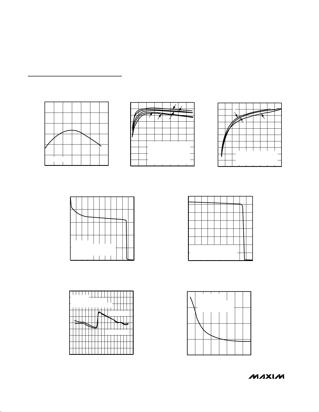
Figure 12. Kelvin Connections for the Current-Sense Resistors
HIGH-CURRENT PATH
SENSE RESISTOR
MAX1667

MAX1667
Chemistry-Independent,
Level 2 Smart Battery Charger
______________________________________________________________________________________ 25
7) The SEL pin digitally limits the output current to 4A,
3A, or 1A without a change in sense resistor value
between the three modes.
8) The single count current-sense voltage has been
changed to 5mV. R1 required is now 40mΩ.
9) After the AlarmWarning() message, the charger is
not locked off. Subsequent ChargingVoltage() or
ChargingCurrent() commands allow the MAX1667
to resume the charge.
10) The Alert-Response address is 0x13 (0b00010011).
When upgrading a MAX1647 design, follow these recommended or required changes (part numbers refer to
Figure 3 of the MAX1647 data sheet):
1) Change R1 to 40mΩ (required).
2) Remove diodes D5 and D6, transistor Q1, and resis-
tor R6. Connect IOUT directly to BATT (recommended).
3) Remove the external +4.096V reference (recom-
mended).
4) Remove D6 (recommended). When doing this, also
place a small-signal diode in series with R7 and connect it directly to the DC source (see D3 and R5 on
Figure 3 of the MAX1647 data sheet).
Pin Configuration
TRANSISTOR COUNT: 6378
SUBSTRATE CONNECTED TO AGND
Chip Information
TOP VIEW
1
IOUT
DCIN
CCV
CCI
SEL
CS
BATT
REF
2
3
VL
4
MAX1667
5
6
7
8
9
10
SSOP
20
19
18
17
16
15
14
13
12
11
BST
LX
DHI
DLO
PGND
DACV
SDA
SCL
THM
INTAGND

MAX1667
Chemistry-Independent,
Level 2 Smart Battery Charger
26 ______________________________________________________________________________________
________________________________________________________Package Information
SSOP.EPS

MAX1667
Chemistry-Independent,
Level 2 Smart Battery Charger
______________________________________________________________________________________ 27
NOTES

Maxim cannot assume responsibility for use of any circuitry other than circuitry entirely embodied in a Maxim product. No circuit patent licenses are
implied. Maxim reserves the right to change the circuitry and specifications without notice at any time.
28
__________________Maxim Integrated Products, 120 San Gabriel Drive, Sunnyvale, CA 94086 (408) 737-7600
© 1999 Maxim Integrated Products Printed USA is a registered trademark of Maxim Integrated Products.
MAX1667
Chemistry-Independent,
Level 2 Smart Battery Charger
NOTES
 Loading...