

19-1158; Rev 0; 12/96
Chemistry-Independent
Battery Chargers
_______________General Description
The MAX1647/MAX1648 provide the power control necessary to charge batteries of any chemistry. In the MAX1647,
all charging functions are controlled via the Intel System
Management Bus (SMBus™) interface. The SMBus 2-wire
serial interface sets the charge voltage and current, and
provides thermal status information. The MAX1647 functions as a level 2 charger, compliant with the Duracell/Intel
Smart Battery Charger Specification. The MAX1648 omits
the SMBus serial interface, and instead sets the charge
voltage and current proportional to the voltage applied to
external control pins.
In addition to the feature set required for a level 2 charger,
the MAX1647 generates interrupts to signal the host when
power is applied to the charger or a battery is installed or
removed. Additional status bits allow the host to check
whether the charger has enough input voltage, and
whether the voltage on or current into the battery is being
regulated. This allows the host to determine when lithiumion batteries have completed charge without interrogating
the battery.
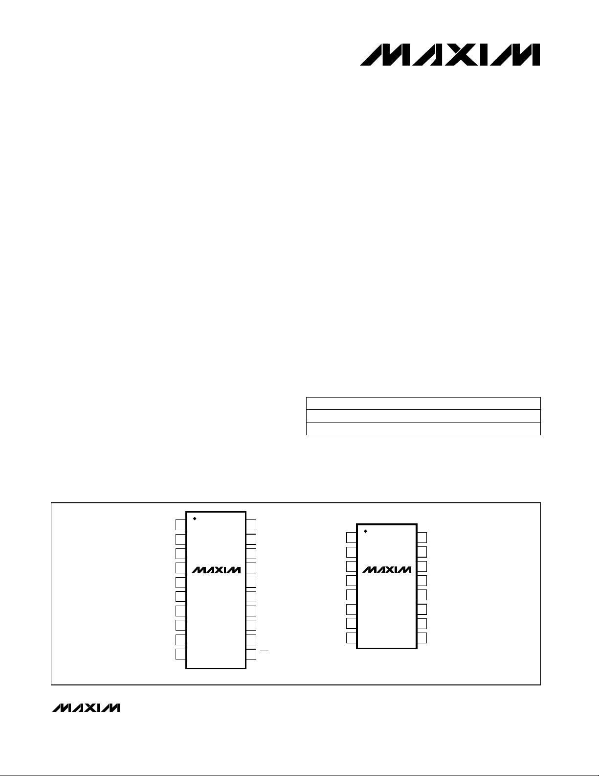
The MAX1647 is available in a 20-pin SSOP with a 2mm
profile height. The MAX1648 is available in a 16-pin SO
package.
________________________Applications
Notebook Computers
Personal Digital Assistants
Charger Base Stations
Phones
____________________________Features
♦ Charges Any Battery Chemistry:
Li-Ion, NiCd, NiMH, Lead Acid, etc.
♦ Intel SMBus 2-Wire Serial Interface (MAX1647)
♦ Intel/Duracell Level 2 Smart Battery Compliant
(MAX1647)
♦ 4A, 2A, or 1A Maximum Battery-Charge Current
♦ 11-Bit Control of Charge Current
♦ Up to 18V Battery Voltage
♦ 10-Bit Control of Voltage
♦ ±0.75% Voltage Accuracy with External ±0.1%
Reference
♦ Up to 28V Input Voltage
♦ Battery Thermistor Fail-Safe Protection
______________Ordering Information
PART
MAX1647EAP
MAX1648ESE
TEMP. RANGE PIN-PACKAGE
-40°C to +85°C
-40°C to +85°C
20 SSOP
16 Narrow SO
MAX1647/MAX1648
__________________________________________________________Pin Configurations
TOP VIEW
IOUT
DCIN
CCV
CCI
SEL
BATT
REF
1
2
3
VL
4
MAX1647
5
6
CS
7
8
9
10
SSOP
20
BST
16
DCIN
CCV
CCI
BATT
REF
AGND
1
VL
2
3
MAX1648
4
CS
5
6
7
8
SO
LX
19
18
DHI
17
DLO
PGND
16
15
DACV
SDA
14
SCL
13
12
THM
11
INTAGND
BST
LX
15
DHI
14
13
DLO
PGND
12
SETV
11
SETI
10
THM
9
SMBus is a trademark of Intel Corp.
________________________________________________________________
Maxim Integrated Products
1
For free samples & the latest literature: http://www.maxim-ic.com, or phone 1-800-998-8800
Chemistry-Independent
Battery Chargers
ABSOLUTE MAXIMUM RATINGS
DCIN to AGND..........................................................-0.3V to 30V
DCIN to IOUT...........................................................-0.3V to 7.5V
BST to AGND............................................................-0.3V to 36V
BST, DHI to LX............................................................-0.3V to 6V
LX to AGND ..............................................................-0.3V to 30V
THM, CCI, CCV, DACV, REF,
DLO to AGND................................................-0.3V to (VL + 0.3V)
VL, SEL, INT, SDA, SCL to AGND (MAX1647) ...........-0.3V to 6V
SETV, SETI to AGND (MAX1648)................................-0.3V to 6V
BATT, CS+ to AGND.................................................-0.3V to 20V
Stresses beyond those listed under “Absolute Maximum Ratings” may cause permanent damage to the device. These are stress ratings only, and functional
operation of the device at these or any other conditions beyond those indicated in the operational sections of the specifications is not implied. Exposure to
absolute maximum rating conditions for extended periods may affect device reliability.
ELECTRICAL CHARACTERISTICS
(V
DCIN
= 18V, V
= 4.096V, TA= 0°C to +85°C. Typical values are at TA= +25°C, unless otherwise noted.)
REF
PGND to AGND.....................................................-0.3V to +0.3V
SDA, INT Current ................................................................50mA
VL Current...........................................................................50mA
Continuous Power Dissipation (T
16-Pin SO (derate 8.7mW/°C above +70°C).................696mW
20-Pin SSOP (derate 8mW/°C above +70°C) ...............640mW
Operating Temperature Range
MAX1647EAP, MAX1648ESE ...........................-40°C to +85°C
Storage Temperature.........................................-60°C to +150°C
Lead Temperature (soldering, 10sec).............................+300°C
= +70°C)
A
MAX1647/MAX1648
SUPPLY AND REFERENCE
LOAD
SWITCHING REGULATOR
BATT Input Current (Note 1)
CS Input Current (Note 1)
CS to BATT Single-Count
Current-Sense Voltage
CS to BATT Full-Scale
Current-Sense Voltage
Voltage Accuracy
MAX1647, SEL = open,
ChargingCurrent( ) = 0x0020
MAX1647, SEL = open,
ChargingCurrent( ) = 0x07F0;
MAX1648, V
MAX1647, ChargingVoltage( ) = 0x1060,
ChargingVoltage( ) = 0x3130; MAX1648,
V
SETV
< 28V, logic inputs = VLDCIN Quiescent Current
DCIN
< 28V, no loadVL Output Voltage
DCIN
= 10mAVL Load Regulation
SOURCE
BATT
BATT
SETI
= 3.15V, V
< 500µAREF Output Voltage
= 12V
= 12V
= 1.024V
SETV
= 1.05V
15VL < 3.2V, V
350 500VL < 5.15V, V
15VL < 3.2V, VCS= 12V
170 400VL < 5.15V, VCS= 12V
-0.65 0.65
UNITSMIN TYP MAXCONDITIONSPARAMETER
V7.5 28DCIN Input Voltage Range
mA467.5V < V
V5.15 5.4 5.657.5V < V
mV100I
V3.20 4 5.15MAX1647VL AC_PRESENT Trip Point
V3.74 3.9 4.070µA < I
µA700REF Overdrive Input Current
kHz200 250 300Oscillator Frequency
%89 93DHI Maximum Duty Cycle
Ω47High or lowDHI On-Resistance
Ω614High or lowDLO On-Resistance
µA
µA
V019BATT, CS Input Voltage Range
mV2.94
mV170 185 200
%
2 _______________________________________________________________________________________
Chemistry-Independent
Battery Chargers
ELECTRICAL CHARACTERISTICS (continued)
(V
= 18V, V
DCIN
ERROR AMPLIFIERS
GMV Amplifier Maximum
Output Current
GMI Amplifier Maximum
Output Current
CCI Clamp Voltage with
Respect to CCV
CCV Clamp Voltage with
Respect to CCI
TRIP POINTS AND LINEAR CURRENT SOURCES
THM THERMISTOR_OR
Over-Range Trip Point
THM THERMISTOR_COLD
Trip Point
THM THERMISTOR_HOT
Trip Point
THM THERMISTOR_UR
Under-Range Trip Point
IOUT Output Current
CURRENT- AND VOLTAGE-SETTING DACs (MAX1647)
SETV, SETI (MAX1648)
LOGIC LEVELS (MAX1647)
Note 1: When DCIN is less than 4V, VL is less than 3.2V, causing the battery current to be typically 2µA (CS plus BATT input
current).
= 4.096V, TA= 0°C to +85°C. Typical values are at TA= +25°C, unless otherwise noted.)
REF
< 3.5V
CCV
< 3.5V
CCI
86.5 89 91.5MAX1647BATT POWER_FAIL Trip Point
89.5 91 92.5MAX1647
74 75.5 77
22 23.5 25
3 4.5 6MAX1647
MAX1647,
V
= 7.5V,
DCIN
V
= 0V
IOUT
= 0.6VSDA Output Low Sink Current
SDA
ChargingCurrent( ) = 0x001F
ChargingCurrent( ) = 0x0000 10 µA
UNITSMIN TYP MAXCONDITIONSPARAMETER
mA/V1.4GMV Amplifier Transconductance
mA/V0.2GMI Amplifier Transconductance
V
µA±80
µA±200
mV25 80 2001.1V < V
mV25 80 2001.1V < V
% of
DCIN
% of
V
REF
% of
V
REF
% of
V
REF
% of
V
REF
mA25 31 35
V-7.5 -1.0With respect to DCIN voltageIOUT Operating Voltage Range
bits6Guaranteed monotonicCDAC Current-Setting DAC Resolution
bits10Guaranteed monotonicVDAC Voltage-Setting DAC Resolution
µA1SETV Input Bias Current
µA5SETI Input Bias Current
V0 4.2SETV Input Voltage Range
V0 1.024SETI Input Voltage Range
V0.8SDA, SCL Input Low Voltage
V2.8SDA, SCL Input High Voltage
µA-1 1SDA, SCL Input Bias Current
mA6V
MAX1647/MAX1648
_______________________________________________________________________________________ 3
Chemistry-Independent
Battery Chargers
ELECTRICAL CHARACTERISTICS
(V
= 18V, V
DCIN
temperature range are guaranteed by design.)
SUPPLY AND REFERENCE
SWITCHING REGULATOR
MAX1647/MAX1648
CS to BATT Full-Scale
Current-Sense Voltage
Voltage Accuracy
ERROR AMPLIFIERS
GMV Amplifier Maximum
Output Current
GMI Amplifier Maximum
Output Current
TRIP POINTS AND LINEAR CURRENT SOURCES
THM THERMISTOR_OR
Over-Range Trip Point
THM THERMISTOR_COLD
Trip Point
THM THERMISTOR_HOT
Trip Point
THM THERMISTOR_UR
Under-Range Trip Point
SETV, SETI (MAX1648)
LOGIC LEVELS (MAX1647)
= 4.096V, TA= -40°C to +85°C. Typical values are at TA= +25°C, unless otherwise noted. Limits over this
REF
< 28V, logic inputs = VLDCIN Quiescent Current
DCIN
< 28V, no loadVL Output Voltage
DCIN
SOURCE
BATT
MAX1647, SEL = open,
ChargingCurrent( ) = 0x07F0;
MAX1648, V
MAX1647, ChargingVoltage( ) = 0x1060,
ChargingVoltage( ) = 0x3130; MAX1648,
V
SETV
SDA
SETI
= 3.15V, V
= 0.6VSDA Output Low Sink Current
< 500µAREF Output Voltage
= 12V
= 1.024V
SETV
= 1.05V
89.5 91 92.5MAX1647
74 75.5 77
22 23.5 25
3 4.5 6MAX1647
UNITSMIN TYP MAXCONDITIONSPARAMETER
mA/V1.4GMV Amplifier Transconductance
mA/V0.2GMI Amplifier Transconductance
mA467.5V < V
V5.15 5.4 5.657.5V < V
V3.74 3.9 4.070µA < I
kHz200 250 310Oscillator Frequency
%89DHI Maximum Duty Cycle
Ω47High or lowDHI On-Resistance
Ω614High or lowDLO On-Resistance
µABATT Input Current 5VL < 3.2V, V
µACS Input Current 5VL < 3.2V, VCS= 12V
mV160 185 200
%-0.65 0.65
µA±130
µA±320
% of
V
REF
% of
V
REF
% of
V
REF
% of
V
REF
µA1SETV Input Bias Current
µA5SETI Input Bias Current
V0.8SDA, SCL Input Low Voltage
V2.8SDA, SCL Input High Voltage
µA-1 1SDA, SCL Input Bias Current
mA6V
4 _______________________________________________________________________________________
Chemistry-Independent
Battery Chargers
TIMING CHARACTERISTICS—MAX1647
(TA= 0°C to +85°C, unless otherwise noted.)
SCL Serial-Clock High Period
SCL Serial-Clock Low Period
Start-Condition Setup Time
Start-Condition Hold Time
SDA Valid to SCL Rising-Edge
Setup Time, Slave Clocking in Data
SCL Falling Edge to SDA Transition
SCL Falling Edge to SDA Valid,
Master Clocking in Data
HIGH
LOW
SU:STA
HD:STA
SU:DAT
HD:DAT
DV
TIMING CHARACTERISTICS—MAX1647
(TA= -40°C to +85°C, unless otherwise noted. Limits over this temperature range are guaranteed by design.)
CONDITIONS
SCL Serial-Clock High Period
SCL Serial-Clock Low Period
Start-Condition Setup Time
Start-Condition Hold Time
SDA Valid to SCL Rising-Edge
Setup Time, Slave Clocking in Data
SCL Falling Edge to SDA Transition
SCL Falling Edge to SDA Valid,
Master Clocking in Data
HIGH
LOW
SU:STA
HD:STA
SU:DAT
HD:DAT
DV
MAX1647/MAX1648
UNITSMIN TYP MAXSYMBOLPARAMETER CONDITIONS
µs4t
µs4.7t
µs4.7t
µs4t
ns250t
ns0t
µs1t
UNITSMIN TYP MAXSYMBOLPARAMETER
µs4t
µs4.7t
µs4.7t
µs4t
ns250t
ns0t
µs1t
_______________________________________________________________________________________ 5
Chemistry-Independent
Battery Chargers
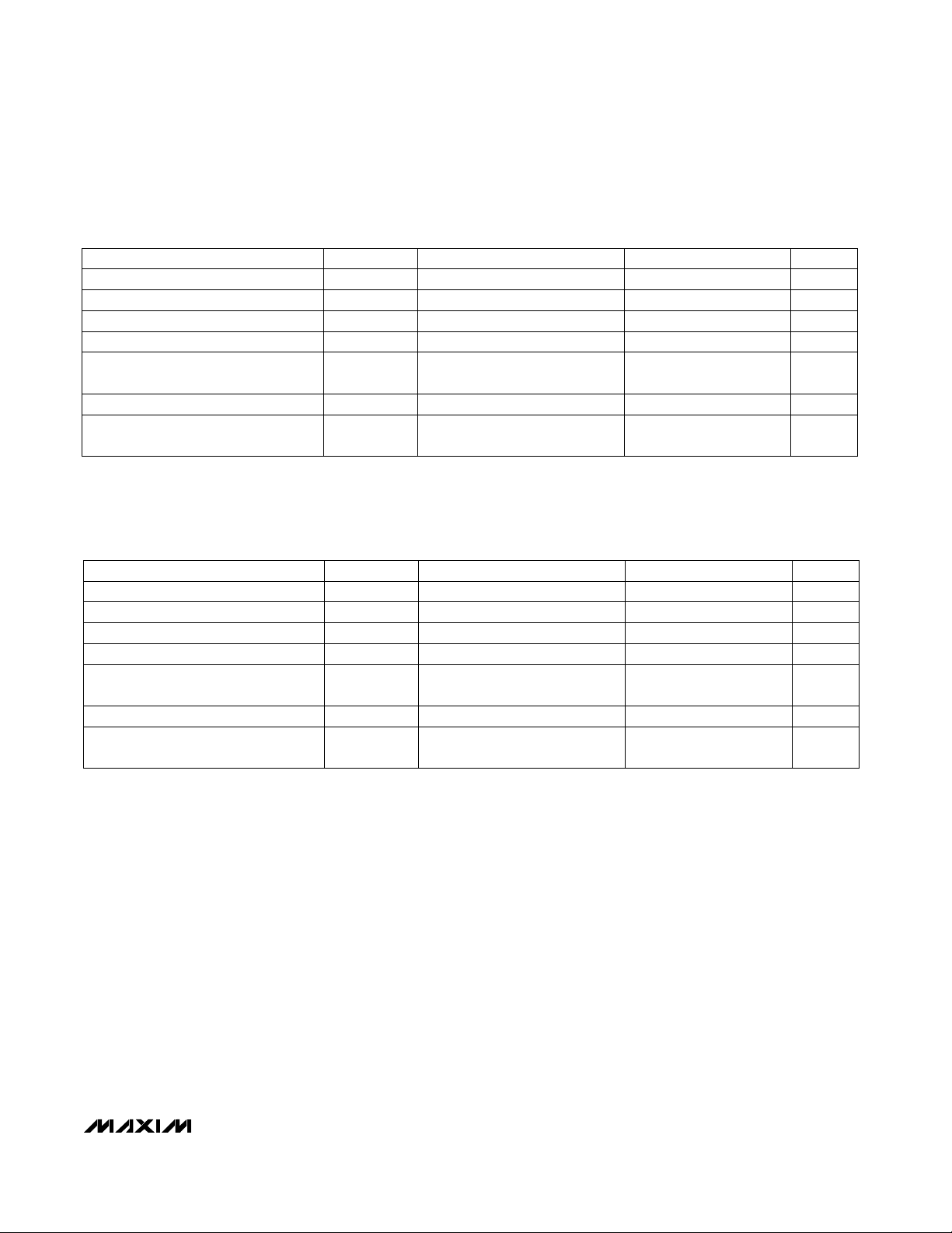
__________________________________________Typical Operating Characteristics
(Circuit of Figure 3, TA = +25°C, unless otherwise noted.)
MAX1647
BATT LOAD TRANSIENT
CCI
CCV
0.9A TO 1.9A TO 0.9A
1ms/div
MAX1647/MAX1648
ChargingVoltage( ) = 0x2EE0 = 12000mV
ChargingCurrent( ) = 0xFFFF = MAX VALUE
ACDCIN = 18.0V, SEL = OPEN, R1 = 0.1Ω
R2 = 10kΩ, C1 = 68µF, C2 = 0.1µF, C3 = 47nF
L1 = 22µH, V
= 4.096V
REF
VL VOLTAGE vs. LOAD CURRENT
5.5
5.0
4.5
VL (V)
4.0
3.5
CIRCUIT OF FIGURE 3
= 6.6V
V
DCIN
0
050
10 20 40
LOAD CURRENT (mA)
30
INPUT AND OUTPUT POWER
40
V
= 28V
DCIN
= 12.6V
V
BATT
35
ChargingCurrent( ) = 0xFFFF
ChargingVoltage( ) = 0xFFFF
30
25
20
POWER (W)
15
10
5
0
500
0 2500
CURRENT INTO BATT (mA)
POWER INTO
CIRCUIT
POWER TO BATT
1000 1500
2000
0.001
MAX1647/48-05
0.01
0.1
DROP IN BATT OUTPUT VOLTAGE (%)
100
MAX1647/48-01
V
2.4V
12V
MAX1647/48-03
CCI
V
CCV
200mV/div
V
BATT
1V/div
CCI
CCV
MAX1647
OUTPUT V-I CHARACTERISTIC
BATT NO-LOAD
OUTPUT VOLTAGE = 16.384V
1
10
V
= 28V, V
DCIN
ChargingVoltage( ) = 0xFFFF
ChargingCurrent( ) = 0xFFFF
500 1000 2000
0 2500
= 4.096V
REF
1500
LOAD CURRENT (mA)
1.1A TO 0.9A TO 1.1A
CCV
ChargingVoltage( ) = 0x2EE0 = 12000mV
ChargingCurrent( ) = 0x03E8 = 1000mA
ACDCIN = 18.0V, SEL = OPEN, C1 = 68µF,
C2 = 0.1µF, C3 = 47nF, R1 = 0.1Ω
R2 = 10kΩ, L1 = 22µH, V
INTERNAL REFERENCE VOLTAGE
3.86
3.84
3.82
3.80
(V)
3.78
REF
V
3.76
3.74
3.72
3.70
0 2.0
MAX1647/48-06
MAX1647
BATT LOAD TRANSIENT
CCI
CCV
CCI
2ms/div
REF
0.5 1.0 1.5
LOAD CURRENT (mA)
MAX1647/48-02
CCV
CCI
= 4.096V
OUTPUT VOLTAGE ERROR
0.8
0.6
0.4
0.2
0
OUTPUT VOLTAGE ERROR (%)
-0.2
-0.4
4500 8500 12,500
PROGRAMMED VOLTAGE CODE IN DECIMAL
3mA LOAD
300mA LOAD
2.3V
12V
MAX1647/48-04
V
CCV
V
CCI
100mV/div
V
BATT
5V/div
16,500
MAX1647/48-07
6 _______________________________________________________________________________________
Chemistry-Independent
Battery Chargers
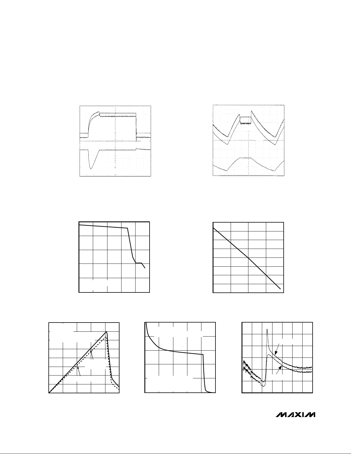
______________________________________________________________Pin Description
PIN
MAX1647 MAX1648
—6 SEL
NAME
INT
Linear Current-Source Output—1 IOUT
Input Voltage for Powering Charger12 DCIN
Chip Power Supply. 5.4V linear regulator output from DCIN.23 VL
Voltage-Regulation-Loop Compensation Point34 CCV
Current-Regulation-Loop Compensation Point45 CCI
Current-Range Selector. Tying SEL to VL sets a 4A full-scale current. Leaving SEL open
sets a 2A full-scale current. Tying SEL to AGND sets a 1A full-scale current.
Current-Sense Positive Input57 CS
Battery Voltage Input and Current-Sense Negative Input68 BATT
3.9V Reference Voltage Output or External Reference Input79 REF
Analog Ground810 AGND
Current-Regulation-Loop Set Point10— SETI
Open-Drain Interrupt Output—11
Voltage-Regulation-Loop Set Point11— SETV
Thermistor Sense Voltage Input912 THM
Serial Clock—13 SCL
Serial Data—14 SDA
Voltage DAC Output—15 DACV
Power Ground1216 PGND
Low-Side Power MOSFET Driver Output1317 DLO
High-Side Power MOSFET Driver Output1418 DHI
Power Connection for the High-Side Power MOSFET Driver1519 LX
Power Connection for the High-Side Power MOSFET Driver1620 BST
FUNCTION
MAX1647/MAX1648
_______________________________________________________________________________________ 7
Chemistry-Independent
Battery Chargers
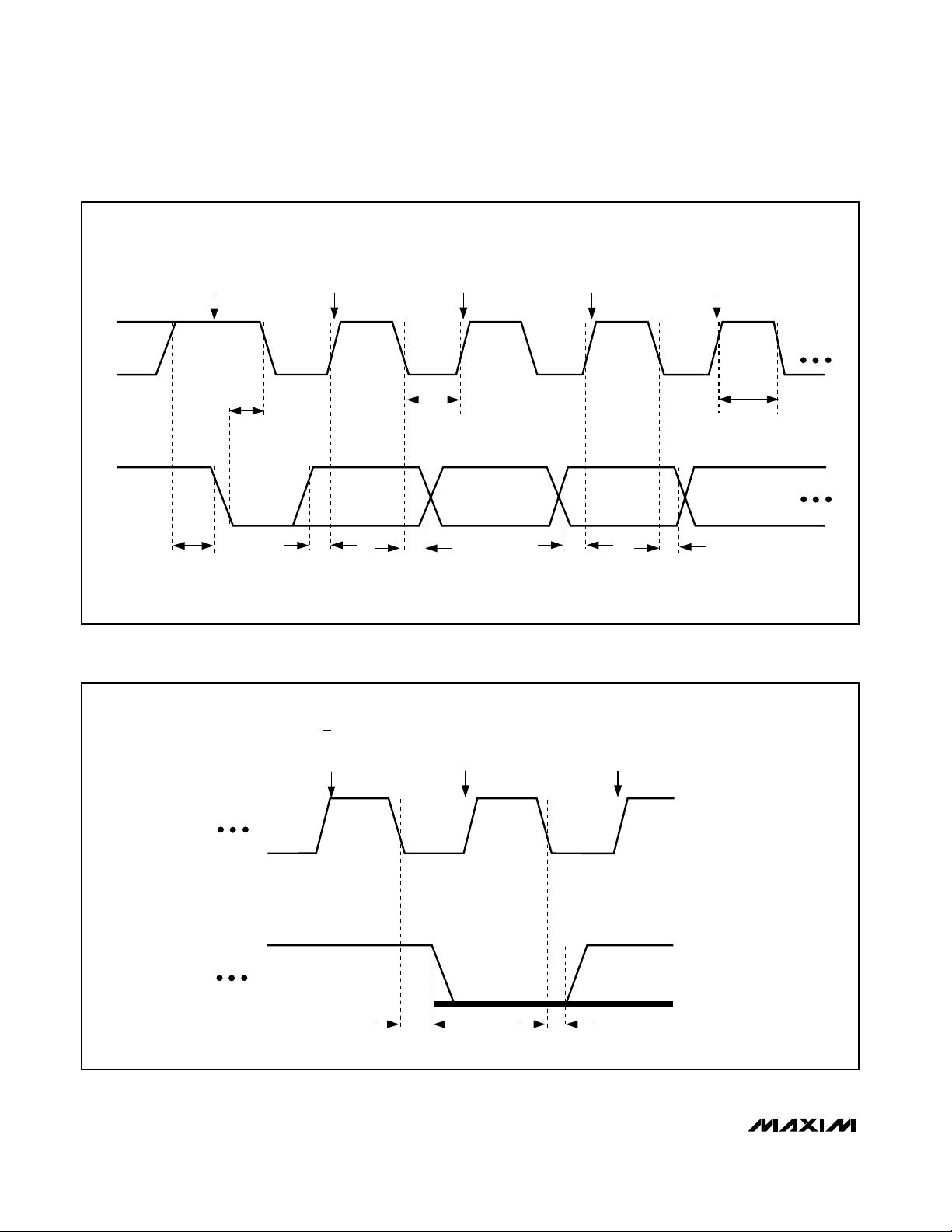
MOST SIGNIFICANT
SCL
START
CONDITION
ADDRESS BIT (A6)
CLOCKED INTO SLAVE
A5 CLOCKED
INTO SLAVE
A4 CLOCKED
INTO SLAVE
A3 CLOCKED
INTO SLAVE
t
HD:STA
SDA
MAX1647/MAX1648
t
SU:STA
Figure 1. SMBus Serial Interface Timing—Address
SCL
t
SU:DAT
RW BIT
CLOCKED
INTO SLAVE
t
HD:DAT
t
LOW
ACKNOWLEDGE
BIT CLOCKED
INTO MASTER
t
SU:DAT
MOST SIGNIFICANT BIT
OF DATA CLOCKED
INTO MASTER
t
HD:DAT
t
HIGH
DV
SLAVE PULLING
SDA LOW
t
DV
SDA
t
Figure 2. SMBus Serial Interface Timing—Acknowledge
8 _______________________________________________________________________________________

Chemistry-Independent
Battery Chargers
MAX1647/MAX1648
4
GND
6
VOUT
MAX874
VIN
2
10
AGND
C4
9
REF
R3
R4
12
THM
MAX1647
5
C3
R2
C2
CCI
4
CCV
IOUT
DCIN
SEL
BST
DHI
DLO
PGND
CS
1
2
6
N.C.
3
VL
C5
(NOTE 2)
20
18
19
LX
17
16
7
Q1
R6
R5
D2
C7
D5
C9
M1
(NOTE 1)
C1
R7
D4*
DC SOURCE
7.5V–28V
L1
D1
D3
D6
C6
M2
15
C8
= HIGH-CURRENT TRACES (8A MAX)
NOTE 1: C6, M2, D1, AND C1 GROUNDS MUST CONNECT TO
THE SAME RECTANGULAR PAD ON THE LAYOUT.
NOTE 2: C5 MUST BE PLACED WITHIN 0.5cm OF THE MAX1647,
WITH TRACES NO LONGER THAN 1cm CONNECTING
VL AND PGND.
*OPTIONAL (SEE
DACV
NEGATIVE INPUT VOLTAGE PROTECTION
BATT
SCL
SDA
INT
SECTION).
Figure 3. MAX1647 Typical Application Circuit
_______________________________________________________________________________________ 9
R1B
8
13
14
11
-TD C+
SMART BATTERY
STANDARD CONNECTOR
SMBDATA
SMBCLOCK
HOST & LOAD
KINT-
GND
R1A

Chemistry-Independent
Battery Chargers
Table 1a. Component Selection for Figure 3 Circuit (Also Use for Figure 4)
UNITSQTYDESIGNATION
µF47C1
µF0.1C2, C4, C7, C9
nF47C3
µF22C6
D1, D3, D4
D2, D5
MAX1647/MAX1648
D6
µH22L1
M1
M2
Q1
20V, ESR at 250kHz ≤ 0.4Ω
10V, ceramic or low ESRµF1C5
35V
10VnF22C8
3A IDC, 30V Schottky diode,
PD> 0.8W, 1N5821 equivalent
50mA IDC, 40V fast-recovery diode,
1N4150 equivalent
4.3V zener diode,
1N4731 or equivalent
±20%, 3A I
Note: size in L x W x H
R
DS, ON
PD> 0.5W, logic level, N-channel
power MOSFET
R
DS, ON
logic level, N-channel power
MOSFET, 2N7002 equivalent
V
CE, MAX
2N3906 equivalent
SAT
≤ 0.1Ω, V
≤ 10Ω, V
≤ -30V, 50mA I
DSS
DSS
≥ 30V,
≥ 30V,
C, CONT
SOURCE/TYPENOTES
Sprague, 595D476X0020D7T, D case
AVX, TPSE476M020R0150, E case
NIEC, NSQ03A04, FLAT-PAK (SMC)
NIEC, 30VQ04F, TO-252AA (SMD)
Motorola, MBRS340T3, SMC
Motorola, MBRD340T4, DPAK
Diodes Inc., SK33, SMC
IR, 30BQ040, SMC
Sumida, RCH-110/220M, 10mm x 10mm x 10mm
Coiltronics, UP2-220, 0.541" x 0.345" x 0.231"
Coilcraft, DO3340P-223, 0.510" x 0.370" x 0.450"
Coilcraft, DO5022P-223, 0.730" x 0.600" x 0.280"
Motorola, MMSF5N03HD, SO-8
Motorola, MMDF3N03HD, SO-8
Motorola, MTD20N03HDL, DPAK
IR, IRF7201, SO-8
IR, IRF7303, SO-8
IR, IRF7603, Micro8
Siliconix, Si9410DY, SO-8
Siliconix, Si9936DY, SO-8
Siliconix, Si6954DQ, TSSOP-8
Motorola, 2N7002LT1, SOT23
Motorola, MMBF170LT1, SOT23
Diodes Inc., 2N7002, SOT23
Diodes Inc., BS870, SOT23
Zetex, ZVN3306F, SOT23
Central Semiconductor, 2N7002, SOT23
,
IRC, CHP1100R100F13, 2512
±1%, 1WmΩ100R1A
±5%, 1/8WΩ1R1B
±5%, 1/16WkΩ10R2, R4
±1%, 1/16WkΩ10R3
±5%, 1/16WΩ10R5, R7
±5%, 1/8WkΩ10R6
10 ______________________________________________________________________________________
IRC, LR251201R100F, 2512
Dale, WSL-2512/0.1Ω/±1%, 2512

Chemistry-Independent
Battery Chargers
Table 1b. Component Suppliers
Central Semiconductor
IR
Sprague
R3
R4
C3
R2
C2
R8
THM
CCI
CCV
SETI
MAX1648
_______________Detailed Description
FAXPHONEMANUFACTURER
(803) 626-3123(803) 946-0690AVX
(516) 435-1824(516) 435-1110
(847) 639-1469(847) 639-6400Coilcraft
(561) 241-9339(561) 241-7876Coiltronics
(605) 665-1627(605) 668-4131Dale
(310) 322-3332(310) 322-3331
(512) 992-3377(512) 992-7900IRC
(805) 867-2698(805) 867-2555NIEC
(408) 970-3950(408) 988-8000Siliconix
(603) 224-1430(603) 224-1961
(847) 956-0702(847) 956-0666Sumida
(516) 864-7630(516) 543-7100Zetex
C4
REF
VL
DCIN
DHI
BST
LX
DLO
PGND
CS
The MAX1647/MAX1648 contain both a voltageregulation loop and a current-regulation loop. Both
loops operate independently of each other. The voltage-regulation loop monitors BATT to ensure that its
voltage never exceeds the voltage set point (V0). The
current-regulation loop monitors current delivered to
BATT to ensure that it never exceeds the current-limit
set point (I0). The current-regulation loop is in control
as long as BATT voltage is below V0. When BATT voltage reaches V0, the current loop no longer regulates,
and the voltage-regulation loop takes over. Figure 5
shows the V-I characteristic at the BATT pin.
C5
R5
D2
C6
M1
C7
M2
Output Characteristics
D4
DC SOURCE
L1
D1
7.5V–28V
D3
R1
MAX1647/MAX1648
R10
R9
SETV
R11
Figure 4. MAX1648 Typical Operating Circuit
______________________________________________________________________________________ 11
BATT
C1
AGND
BATTERY
T

Chemistry-Independent
Battery Chargers
BATT
VOLTAGE
V0
V0 = VOLTAGE SET POINT
I0 = CURRENT-LIMIT SET POINT
AVERAGE CURRENT
THROUGH THE RESISTOR
I0
BETWEEN CS AND BATT
MAX1647/MAX1648
Figure 5. Output V-I Characteristic
Setting V0 and I0 (MAX1647)
Set the MAX1647’s voltage and current-limit set points
via the Intel System Management Bus (SMBus™) 2-wire
serial interface. The MAX1647’s logic interprets the
serial-data stream from the SMBus interface to set internal digital-to-analog converters (DACs) appropriately.
See the
Set the MAX1648’s voltage- and current-limit set points
(V0 and I0, respectively) using external resistive dividers.
Figure 6b is the MAX1648 block diagram. V0 equals four
times the voltage on the SETV pin. I0 equals the voltage
on SETI divided by 5.5, divided by R1 (Figure 4).
_____________________Analog Section
The MAX1647/MAX1648 analog section consists of a
current-mode PWM controller and two transconductance error amplifiers: one for regulating current and
the other for regulating voltage. The MAX1647 uses
DACs to set the current and voltage level, which are
controlled via the SMBus interface. The MAX1648 eliminates the DACs and controls the error amplifiers directly from SETI (for current) and SETV (for voltage). Since
separate amplifiers are used for voltage and current
control, both control loops can be compensated separately for optimum stability and response in each state.
The following discussion relates to the MAX1647; however, MAX1648 operation can easily be inferred from
the MAX1647.
MAX1647 Logic
Setting V0 and I0 (MAX1648)
section for more information.
Whether the MAX1647 is controlling the voltage or current at any time depends on the battery’s state. If the
battery has been discharged, the MAX1647’s output
reaches the current-regulation limit before the voltage
limit, causing the system to regulate current. As the battery charges, the voltage rises until the voltage limit is
reached, and the charger switches to regulating voltage.
The transition from current to voltage regulation is done
by the charger, and need not be controlled by the host.
Voltage Control
The internal GMV amplifier controls the MAX1647’s output voltage. The voltage at the amplifier’s noninverting
input amplifier is set by a 10-bit DAC, which is controlled
by a ChargingVoltage( ) command on the SMBus (see
the
MAX1647 Logic
battery voltage is fed to the GMV amplifier through a 4:1
resistive voltage divider. With an external 4.096V reference, the set voltage ranges between 0 and 16.38V with
16mV resolution.
This poses a challenge for charging four lithium-ion
cells in series: because the lithium-ion battery’s typical
per-cell voltage is 4.2V maximum, 16.8V is required. A
larger reference voltage can be used to circumvent
this. Under this condition, the maximum battery voltage
no longer matches the programmed voltage. The solution is to use a 4.2V reference and host software.
Contact Maxim’s applications department for more
information.
The GMV amplifier’s output is connected to the CCV
pin, which compensates the voltage-regulation loop.
Typically, a series-resistor/capacitor combination can
be used to form a pole-zero couplet. The pole introduced rolls off the gain starting at low frequencies. The
zero of the couplet provides sufficient AC gain at midfrequencies. The output capacitor then rolls off the midfrequency gain to below 1, to guarantee stability before
encountering the zero introduced by the output capacitor’s equivalent series resistance (ESR). The GMV
amplifier’s output is internally clamped to between onefourth and three-fourths of the voltage at REF.
section for more information). The
Current Control
The internal GMI amplifier and an internal current
source control the battery current while the charger is
regulating current. Since the regulator current’s accuracy is not adequate to ensure full 11-bit accuracy, an
internal linear current source is used in conjunction with
the PWM regulator to set the battery current. The current-control DAC’s five least significant bits set the
12 ______________________________________________________________________________________

REF
10k 10k
10k
10k
Chemistry-Independent
Battery Chargers
16mA
8mA 4mA 2mA 1mA
DCIN
MAX1647/MAX1648
THM
AGND
CS
BATT
FROM LOGIC
BLOCK
FROM LOGIC BLOCK
BATT
FROM LOGIC BLOCK
100k
CURRENT-SENSE
LEVEL SHIFT AND
GAIN OF 5.5
REF
6
6-BIT DAC
AGND
R
RR
AGND
30k 3k
TO LOGIC BLOCK
TO LOGIC BLOCK
R
10
10-BIT DAC
REF
THERMISTOR_OR
THERMISTOR_COLD
LOGIC
BLOCK
THERMISTOR_HOT
THERMISTOR_UR
500Ω
NOTE: APPROX. REF/4 + V
TO 3/4 REF + V
CCI
R
R
R
VOLTAGE_INREG
CURRENT_INREG
GMI
R
GMV
DACV
CLAMP
CCV
CCV_LOW
3/8 REF = ZERO CURRENT
NOTE: REF/4 TO 3/4 REF
MIN
THERM_SHUT
AC_PRESENT
THRESH
THRESH
CLAMP
TO REF
(MAX)
AGND
5
SEL
SCL
SDA
INT
COMPARATOR
FROM LOGIC
BLOCK
SHUTDOWN
5.4V LINEAR
REGULATOR
R
AGND
SUMMING
BLOCK
THERMAL
DCIN
3R
LEVEL
SHIFT
VL
AGND
CCV
REF
INTERNAL 3.9V
REFERENCE
BST
DRIVER
LX
VL
DRIVER
PGND
IOUT
REF
DHI
DLO
AGND
Figure 6a. MAX1647 Block Diagram
______________________________________________________________________________________ 13
TO LOGIC BLOCK
POWER_FAIL
DCIN/4.5

Chemistry-Independent
Battery Chargers
REF
THM
MAX1647/MAX1648
AGND
CS
BATT
CURRENT-SENSE
LEVEL SHIFT AND
GAIN OF 5.5
BATT
AGND
ON
SETI
R
R
RR
SETV
GMI
GMV
10k
30k
CLAMP
CCI
CCV
10k
3k
MIN
AC_PRESENT
REF / 2 =
ZERO CURRENT
NOT (THERMISTOR_HOT
OR THERMISTOR_COLD)
THERMISTOR_COLD
THERMISTOR_HOT
DCIN
5.4V LINEAR
REGULATOR
SUMMING
COMPARATOR
BLOCK
ON
AC_PRESENT AND
LEVEL
SHIFT
VL
AGND
INTERNAL 3.9V
REFERENCE
BST
DRIVER
LX
VL
DRIVER
PGND
REF
DHI
DLO
Figure 6b. MAX1648 Block Diagram
14 ______________________________________________________________________________________

Chemistry-Independent
Battery Chargers
internal current sources’ state, and the six most significant bits control the switching regulator’s current. The
internal current source supplies 1mA resolution to the
battery to comply with the smart-battery specification.
When the current is set to a number greater than 32,
the internal current source remains at 31mA. This guarantees that battery-current setting is monotonic regardless of current-sense resistor choice and current-sense
amplifier offset.
The GMI amplifier’s noninverting input is driven by a 4:1
resistive voltage divider, which is driven by the 6-bit
DAC. If an external 4.096V reference is used, this input
is approximately 1.0V at full scale, and the resolution is
16mV. The current-sense amplifier drives the inverting
input to the GMI amplifier. It measures the voltage
across the current-sense resistor (R
between the CS and BATT pins), amplifies it by approximately 5.45, and level shifts it to ground. The full-scale
current is approximately 0.2V / R
is 3.2mV / R
The current-regulation-loop is compensated by adding
a capacitor to the CCI pin. This capacitor sets the current-feedback loop’s dominant pole. The GMI amplifier’s
output is clamped to between approximately one-fourth
and three-fourths of the REF voltage. While the current is
in regulation, the CCV voltage is clamped to within
80mV of the CCI voltage. This prevents the battery voltage from overshooting when the DAC voltage setting is
updated. The converse is true when the voltage is in
regulation and the current is not at the current DAC setting. Since the linear range of CCI or CCV is about 1.5V
to 3.5V or about 2V, the 80mV clamp results in a relatively negligible overshoot when the loop switches from
voltage to current regulation or vice versa.
SEN
.
, and the resolution
SEN
) (which is
SEN
PWM Controller
The battery voltage or current is controlled by the current-mode, pulse-width-modulated (PWM), DC-DC converter controller. This controller drives two external
N-channel MOSFETs, which switch the voltage from the
input source. This switched voltage feeds an inductor,
which filters the switched rectangular wave. The controller sets the pulse width of the switched voltage so that
it supplies the desired voltage or current to the battery.
The heart of the PWM controller is the multi-input comparator. This comparator sums three input signals to
determine the pulse width of the switched signal, setting the battery voltage or current. The three signals are
the current-sense amplifier’s output, the GMV or GMI
error amplifier’s output, and a slope-compensation signal, which ensures that the controller’s internal currentcontrol loop is stable.
The PWM comparator compares the current-sense
amplifier’s output to the higher output voltage of either
the GMV or the GMI amplifier (the error voltage). This
current-mode feedback corrects the duty ratio of the
switched voltage, regulating the peak battery current
and keeping it proportional to the error voltage. Since
the average battery current is nearly the same as the
peak current, the controller acts as a transconductance
amplifier, reducing the effect of the inductor on the output filter LC formed by the output inductor and the battery’s parasitic capacitance. This makes stabilizing the
circuit easy, since the output filter changes from a complex second-order RLC to a first-order RC. To preserve
the inner current-control loop’s stability, slope compensation is also fed into the comparator. This damps out
perturbations in the pulse width at duty ratios greater
than 50%.
At heavy loads, the PWM controller switches at a fixed
frequency and modulates the duty cycle to control the
battery voltage or current. At light loads, the DC current
through the inductor is not sufficient to prevent the current from going negative through the synchronous rectifier (Figure 3, M2). The controller monitors the current
through the sense resistor R
the synchronous rectifier turns off to prevent negative
current flow.
; when it drops to zero,
SEN
MOSFET Drivers
The MAX1647 drives external N-channel MOSFETs to
regulate battery voltage or current. Since the high-side
N-channel MOSFET’s gate must be driven to a voltage
higher than the input source voltage, a charge pump is
used to generate such a voltage. The capacitor C7
(Figure 3) charges to approximately 5V through D2
when the synchronous rectifier turns on. Since one side
of C7 is connected to the LX pin (the source of M1), the
high-side driver (DHI) can drive the gate up to the voltage at BST, which is greater than the input voltage,
when the high-side MOSFET turns on.
The synchronous rectifier behaves like a diode, but with
a smaller voltage drop to improve efficiency. A small
dead time is added between the time that the high-side
MOSFET turns off and the synchronous rectifier turns
on, and vice versa. This prevents crowbar currents (currents that flow through both MOSFETS during the brief
time that one is turning on and the other is turning off).
Connect a Schottky rectifier from ground to LX (across
the source and drain of M2) to prevent the synchronous
rectifier’s body diode from conducting. The body diode
typically has slower switching-recovery times, so allowing it to conduct would degrade efficiency.
MAX1647/MAX1648
______________________________________________________________________________________ 15

Chemistry-Independent
Battery Chargers
The synchronous rectifier may not be completely
replaced by a diode because the BST capacitor
charges while the synchronous rectifier is turned on.
Without the synchronous rectifier, the BST capacitor
may not fully charge, leaving the high-side MOSFET
with insufficient gate drive to turn on. However, the synchronous rectifier may be replaced with a small MOSFET, such as a 2N7002, to guarantee that the BST
capacitor is allowed to charge. In this case, most of the
current at high currents is carried by the diode and not
by the synchronous rectifier.
Internal Regulator and Reference
The MAX1647 uses an internal low-dropout linear regulator to create a 5.4V power supply (VL), which powers its
internal circuitry. VL can supply up to 20mA. A portion of
this current powers the internal circuitry, but the remaining current can power the external circuitry. The current
used to drive the MOSFETs comes from this supply,
MAX1647/MAX1648
which must be considered when calculating how much
power can be drawn. To estimate the current required to
drive the MOSFETs, multiply the total gate charge of
each MOSFET by the switching frequency (typically
250kHz). The internal circuitry requires as much as 6mA
from the VL supply. To ensure VL stability, bypass the VL
pin with a 1µF or greater capacitor.
The MAX1647 has an internal ±2% accurate 3.9V reference voltage. An external reference can be used to
increase the charger’s accuracy. Use a 4.096V reference,
such as the MAX874, for compliance with the Intel/
Duracell smart-battery specification. Voltage-setting
accuracy is ±0.65%, so the total voltage accuracy is the
accuracy added to the reference accuracy. For 1% total
voltage accuracy, use a reference with ±0.35% or greater
accuracy. If the internal reference is used, bypass it with
a 0.1µF or greater capacitor.
MAX1647 Logic
The MAX1647 uses serial data to control its operation. The
serial interface complies with the SMBus specification (see
System Management Bus Specification
Architecture Labs; http://www.intel.com/IAL/powermgm.html; Intel Architecture Labs: 800-253-3696).
Charger functionality complies with the Intel/Duracell
Smart Charger Specification for a level 2 charger.
The MAX1647 uses the SMBus Read-Word and WriteWord protocols to communicate with the battery it is
charging, as well as with any host system that monitors
the battery to charger communications. The MAX1647
never initiates communication on the bus; it only
receives commands and responds to queries for status
information. Figure 7 shows examples of the SMBus
Write-Word and Read-Word protocols.
, from Intel
ACK
D10
D11
D12
D13
D14
D15
ACK
ACK
CMD0
CMD1
CMD2
CMD3
CMD4
CMD5
CMD6
CMD7
ACK
START
TIME
D8
D9
D0
D1
D2
D3
D4
D5
D6
D7
W
1
0
0
1
0
0
0
SCL
SDA
BOLD LINE INDICATES THAT
THE MAX1647 PULLS SDA LOW
ChargingMode( ) = 0 x 12
ChargingVoltage( ) = 0 x 15
ChargingCurrent( ) = 0 x 14
AlarmWarning( ) = 0 x 16
ChargerStatus( ) = 0 x 13
ACK
THERMISTOR_OR
THERMISTOR_COLD
THERMISTOR_HOT
THERMISTOR_UR
ALARM_INHIBITED
POWER_FAIL
BATTERY_PRESENT
AC_PRESENT
ACK
1
1
0
0
1
0
0
0
ACK
W
1
0
0
1
0
0
0
WRITE WORD: ChargingMode( ), ChargingVoltage( ), ChargingCurrent( ), AlarmWarning( )
START
SCL
CHARGE_INHIBITED
MASTER_MODE
VOLTAGE_NOTREG
CURRENT_NOTREG
SDA
ACK
LEVEL_2
LEVEL_3
CURRENT_OR
VOLTAGE_OR
ACK
REPEATED
START
Figure 7. Write-Word and Read-Word Examples
R
1
0
0
1
0
0
0
SCL
SDA
READ WORD: ChargersStatus( )
16 ______________________________________________________________________________________

Chemistry-Independent
Battery Chargers
Each communication with the MAX1647 begins with a
start condition that is defined as a falling edge on SDA
with SCL high. The device address follows the start
condition. The MAX1647 device address is 0b0001001
(0b indicates a binary number), which may also be
denoted as 0x12 (0x indicates a hexadecimal number)
for Write-Word commands, or 0x13 in hexadecimal for
Read-Word commands (note that the address is only
seven bits, and the hexadecimal representation uses
R/W as its least significant bit).
ChargerMode( )
The ChargerMode( ) command uses Write-Word protocol. The command code for ChargerMode( ) is 0x12;
thus the CMD7–CMD0 bits in Write-Word protocol
should be 0b00010010. Table 2 describes the functions
of the 16 different data bits (D0–D15). Bit 0 refers to the
D0 bit in the Write-Word protocol (Figure 7).
Whenever the BATTERY_PRESENT status bit is clear,
the HOT_STOP bit is set, regardless of any previous
ChargerMode( ) command. To charge a battery that
has a thermistor impedance in the HOT range (i.e.,
THERMISTOR_HOT = 1 and THERMISTOR_UR = 0),
the host must use the ChargerMode( ) command to
clear HOT_STOP after the battery is inserted. The
HOT_STOP bit returns to its default power-up condition
(‘1’) whenever the battery is removed.
ChargingVoltage( )
The ChargingVoltage( ) command uses Write-Word
protocol. The command code for ChargingVoltage( ) is
0x15; thus, the CMD7–CMD0 bits in Write-Word protocol should be 0b00010101. The 16-bit binary number
formed by D15–D0 represents the voltage set point
(V0) in millivolts; however, since the MAX1647 has only
16mV resolution in setting V0, the D0, D1, D2, and D3
bits are ignored. For D15 = D14 = 0:
VOLTAGE_OR = 0 and V0 in Volts = 4 x REF x
()
VDAC
10
2
In equation 1, VDAC is the decimal equivalent of the
binary number represented by bits D13, D12, D11,
D10, D9, D8, D7, D6, D5, and D4 programmed with the
ChargingVoltage( ) command. For example, if D4–D13
are all set, VDAC is the decimal equivalent of
0b1111111111 (1023). If either D15 or D14, or both
D15 and D14, are set, all the bits in the voltage DAC
(Figure 6a) are set, regardless of D13–D0, and the
status register’s VOLTAGE_OR bit is set. For D15 = 1
and/or D14 = 1:
10
VOLTAGE_OR = 1 and V0 in Volts = 4 x REF x
()
2-1
10
2
MAX1647/MAX1648
Table 2. ChargerMode( ) Bit Functions
BIT NAME
ENABLE_POLLING
N/A
BATTERY_PRESENT_MASK
*
Bit position in the D15–D0 data.
N/A = Not available.
______________________________________________________________________________________ 17
BIT
POSITION*
4, 7, 8, 9,
11–15
**
Power-on reset value.
POR
VALUE**
00INHIBIT_CHARGE
—1
—2POR_RESET
—3RESET_TO_ZERO
—
05
16POWER_FAIL_MASK
110HOT_STOP
FUNCTION
0 = Allow normal operation; clear the CHG_INHIBITED status bit.
1 = Turn the charger off; set the CHG_INHIBITED status bit.
Not implemented. Write 0 into this bit.
0 = No change in any non-ChargerMode( ) settings.
1 = Change the voltage and current settings to 0xFFFF and 0x00C0
respectively; clear the THERMISTOR_HOT and ALARM_INHIBITED bits.
Not implemented. Write 0 into this bit.
Not implemented. Write 1 into this bit.
0 = Interrupt on either edge of the BATTERY_PRESENT status bit.
1 = Do not interrupt because of a BATTERY_PRESENT bit change.
0 = Interrupt on either edge of the POWER_FAIL status bit.
1 = Do not interrupt because of a POWER_FAIL bit change.
0 = The THERMISTOR_HOT status bit does not turn the charger off.
1 = THERMISTOR_HOT turns the charger off.

Chemistry-Independent
Battery Chargers
Figure 8 shows the mapping between V0 (the voltageregulation-loop set point) and the ChargingVoltage( )
data.
The power-on reset value for the ChargingVoltage( )
register is 0xFFF0; thus, the first time a MAX1647 is
powered on, the BATT voltage regulates to 16.368V
with V
= 4.096V. Any time the BATTERY_PRESENT
REF
status bit is clear, the ChargingVoltage( ) register
returns to its power-on reset state.
16.368
MAX1647/MAX1648
V
= 4.096V
REF
12.592
ChargingCurrent( )
The ChargingCurrent( ) command uses Write-Word
protocol. The command code for ChargingCurrent( ) is
0x14; thus, the CMD7–CMD0 bits in Write-Word protocol should be 0b00010100. The 16-bit binary number
formed by D15–D0 represents the current-limit set point
(I0) in milliamps. Tying SEL to AGND selects a 1.023A
maximum setting for I0. Leaving SEL open selects a
2.047A maximum setting for I0. Tying SEL to VL selects
a 4.095A maximum setting for I0.
8.400
VOLTAGE SET POINT (V0)
4.192
0
0b000000000000xxxx
0x000x
Figure 8. ChargingVoltage( ) Data to Voltage Mapping
18 ______________________________________________________________________________________
0b000100000110xxxx
0x106x
0b001000001101xxxx
0x20Dx 0x3FFx
ChargingVoltage( ) D15–D0 DATA
0b001100010011xxxx
0x313x
0b001111111111xxxx
0b111111111111xxxx
0xFFFx

Chemistry-Independent
Battery Chargers
Two sources of current in the MAX1647 charge the battery: a binary-weighted linear current source sources
from IOUT, and a switching regulator controls the current
flowing through the current-sense resistor (R1). IOUT
provides a small maintenance charge current to compensate for battery self-discharge, while the switching
regulator provides large currents for fast charging.
IOUT sources from 1mA to 31mA. Table 3 shows the
relationship between the value programmed with the
ChargingCurrent( ) command and IOUT source current.
The CCV_LOW comparator checks to see if the output
voltage is too high by comparing CCV to REF / 4. If
CCV_LOW = 1 (when CCV < REF / 4), IOUT shuts off,
preventing the output voltage from exceeding the voltage
set point specified by the ChargingVoltage( ) register.
VOLTAGE_NOTREG = 1 whenever the internal clamp
pulls down on CCV. (The internal clamp pulls down on
CCV to keep its voltage close to CCI’s voltage.)
Table 3. Relationship Between IOUT Source Current and ChargingCurrent( ) Value
CHARGE_
INHIBITED
(NOTE 1)
ALARM_
INHIBITED
000
000
000
000
000
000
000
000
1x0
x10
xx1
ChargingVoltage( )
0x0010–0xFFFF
0x0010–0xFFFF
0x0010–0xFFFF
0x0010–0xFFFF
0x0010–0xFFFF
0x0010–0xFFFF
x
0x0000–0x000F
x
x
x
ChargingCurrent( )
0x0001–0x001F
0x0001–0x001F
0x0001–0x001F
0x0020–0xFFFF
0x0020–0xFFFF
0x0020–0xFFFF
0x0000
x
x
x
x
CCV_LOW
0
1
1
0
1
1
x
x
x
x
x
VOLTAGE_
NOTREG
x
0
1
x
0
1
x
x
x
x
x
OUTPUT
CURRENT
1mA–31mA
1mA–31mA
MAX1647/MAX1648
IOUT
0mA
31mA
0mA
31mA
0mA
0mA
0mA
0mA
0mA
Note 1: Logical AND of THERMISTOR_HOT, HOT_STOP, NOT(THERMISTOR_UR).
185
SEL = OPEN OR SEL = VL
94
AVERAGE CS - BATT VOLTAGE
IN CURRENT REGULATION (mV)
2.94
0b000001 0b100000 0b111111
CURRENT DAC CODE, DA5–DA0 BITS
Figure 9. Average Voltage Between CS and BATT vs. Current DAC Code
______________________________________________________________________________________ 19

Chemistry-Independent
Battery Chargers
Table 4. Relationship Between Current DAC Code and the ChargingCurrent( ) Value
CHARGE_
INHIBITED
0
0
(NOTE 1)
MAX1647/MAX1648
0
0
Note 1: Logical AND of THERMISTOR_HOT, HOT_STOP, NOT(THERMISTOR_UR).
Note 2: Value of CURRENT_OR bit in the ChargerStatus( ) register.
N/C = No change
ALARM_
INHIBITED
000
000
000
000
000
ChargingVoltage( )
0x0010–0xFFFF
0x0010–0xFFFF
0x0010–0xFFFF
0x0010–0xFFFF
0x0010–0xFFFF 0x0040–0x07DF
0x0010–0xFFFF
0x0010–0xFFFF
0x0010–0xFFFF 0x0020–0x003F
0x0010–0xFFFF
0x0010–0xFFFF
0x0010–0xFFFF 0x0FC0–0x0FFF
0x0010–0xFFFF
0x0010–0xFFFF
x
x x
SEL
open0x0010–0xFFFF 0x0001–0x001F
open
open
open
open0x0010–0xFFFF 0x0800–0xFFFF
ChargingCurrent( )
0V
0V0x0010–0xFFFF 0x0020–0x003F 2 Yes 0000
0V
0V0x0010–0xFFFF 0x03E0–0x03FF
0V
VL
VL
VL
VL0x0010–0xFFFF 0x0080–0x0F9F
VL
VL
VL
xx 0x0000
x
xx x
x
x
0x0001–0x001F
0x0040–0x03DF 4–60 Yes 0000
0x0400–0xFFFF
0x0020–0x003F
0x07E0–0x07FF
0x0001–0x001F
0x0040–0x007F
0x0FA0–0x0FBF
0x0001–0xFFFF 63 Yes 1000
x
x
CURRENT
DAC
CODE
0
62 Yes 0000
62
0 No 0000
1 Yes 000
2–62 Yes
63
63 Yes 1000
0 No 000
1 Yes
1
2–62 Yes 0000
63 Yes 000
63 Yes
0 No 0000
N/C
N/C No N/C1x0
N/C No N/Cx1
N/C No
SW REG
ON?
No
Yes
Yes
Yes
No
(NOTE 2)
0
1
0000
0
0000
0
0000
N/C
N/Cxx1
Table 5. Effect of SEL Pin-Strapping on the ChargingCurrent( ) Data Bits
SEL
Open
*
When SEL = VL, D5 = 1 forces DA0 to be 1 regardless of the D6 bit value.
With the switching regulator on, the current through R1
(Figure 3) is regulated by sensing the average voltage
between CS and BATT. A 6-bit current DAC controls
the current-limit set point. DA5–DA0 denote the bits in
the current DAC code. Figure 9 shows the relationship
between the current DAC code and the average voltage between CS and BATT.
20 ______________________________________________________________________________________
R1
(mΩ)
181AGND
90
45VL
D15
0
0
0
D14
0
0
0
D13
0
0
0
D12
0
0
0
D11
0
0
DA5
D10
0
DA5
DA4
D9
DA5
DA4
DA3
D8
D7
D6
D5
D4
D3
DA4
DA3
DA2
DA3
DA2
DA2
DA1
DA1
DA0
DA1
DA0
I4
I3
I4
I3
*
I4
I3
When the switching regulator is off, DHI is forced to
LX and DLO is forced to ground. This prevents current
from flowing through inductor L1. Table 4 shows the
relationship between the ChargingCurrent( ) register
value and the switching regulator current DAC code.
D2
I2
I2
I2
D1
I1
I1
I1
D0
I0
I0
I0

Chemistry-Independent
Battery Chargers
With SEL = AGND, R1 should be as close as possible to
0.185 / 1.023 = 181mΩ to ensure that the actual output
current matches the data value programmed with the
ChargingCurrent( ) command. With SEL = open, R1
should be as close as possible to 90mΩ. With SEL = VL,
R1 should be as close as possible to 45mΩ. Table 5 summarizes how SEL affects the R1 value and the meaning of
data bits D15–D0 in the ChargingCurrent( ) command.
DA5–DA0 denote the current DAC code bits, and I4–I0
denote the IOUT linear-current source binary weighting
bits. Note that whenever any current DAC bits are set, the
linear-current source is set to full scale (31mA).
The power-on reset value for the ChargingCurrent( )
register is 0x000C. Irrespective of the SEL pin setting,
the MAX1647 powers on with I0 set to 12mA (i.e.,
DA5–DA0, I1, and I0 all equal to zero, and only I3 and
I2 set). Anytime the BATTERY_PRESENT status bit is
clear (battery removed), the ChargingCurrent( ) register
returns to its power-on reset state. This ensures that
upon insertion of a battery, the initial charging current is
12mA.
AlarmWarning( )
The AlarmWarning( ) command uses Write-Word protocol.
The command code for AlarmWarning( ) is 0x16; thus the
CMD7–CMD0 in Write-Word protocol should be
0b00010110. The AlarmWarning( ) command sets the
ALARM_INHIBITED status bit in the MAX1647 if D15, D14,
or D12 of the Write-Word protocol data equals 1. Table 6
summarizes the AlarmWarning( ) command’s function.
The ALARM_INHIBITED status bit remains set until
BATTERY_PRESENT = 0 (battery removed) or a
ChargerMode() command is written with the POR_RESET
bit set. As long as ALARM_INHIBITED = 1, the MAX1647
switching regulator and IOUT current source remain off.
ChargerStatus( )
The ChargerStatus( ) command uses Read-Word protocol. The command code for ChargerStatus( ) is 0x13;
thus, the CMD7–CMD0 bits in Write-Word protocol
should be 0b00010011. The ChargerStatus( ) command returns information about thermistor impedance
and the MAX1647’s internal state. The Read-Word
protocol returns D15–D0 (Figure 7). Table 7 describes
the meaning of the individual bits. The latched bits,
THERMISTOR_HOT and ALARM_INHIBITED, are
cleared whenever BATTERY_PRESENT = 0 or
ChargerMode( ) is written with POR_RESET = 1.
Interrupts and the Alert-Response
Address
An interrupt is triggered (INT goes low) whenever power
is applied to DCIN, the BATTERY_PRESENT bit changes,
or the POWER_FAIL bit changes. BATTERY_PRESENT
and POWER_FAIL have interrupt masks that can be set
or cleared via the ChargerMode( ) command. INT stays
low until the interrupt is cleared. There are two methods
for clearing the interrupt: issuing a ChargerStatus( ) command, and using the Receive Byte protocol with a 0x19
Alert-Response address. The MAX1647 responds to the
Alert-Response address with the 0x89 byte.
__________Applications Information
Using the MAX1647
with Duracell Smart Batteries
The following pseudo-code describes an interrupt routine that is triggered by the MAX1647 INT output going
low. This interrupt routine keeps the host informed of
any changes in battery-charger status, such as DCIN
power detection, or battery removal and insertion.
DOMAX1647:
{ This is the beginning of the routine that handles
MAX1647 interrupts. }
{ Check the status of the MAX1647. }
TEMPWORD = ReadWord( SMBADDR = 0b00010011
= 0x13, COMMAND = 0x13 )
{ Check for the normal power-up case without a battery
installed. THERMISTOR_OR = 1, BATTERY_PRESENT =
0. Use 0b1011111011111111 = 0xBEFF as the mask. }
IF (TEMPWORD OR 0xBEFF) = 0xBFFF THEN GOTO
NOBATT:
{ Check to see if the battery is installed. BATTERY_
PRESENT = 1. Use 0b1011111111111111 = 0xBFFF as
the mask. }
MAX1647/MAX1648
Table 6. Effect of the AlarmWarning( ) Command
AlarmWarning( ) WRITE-WORD PROTOCOL DATA
D15 D14 D13 D12 D11 D10 D9 D8 D7 D6 D5 D4 D3 D2 D1 D0
1
x
x
x
x
x
x
x
x
x
x
x
x
x
x
x
1
x
x
x
x
x
x
x
x
x
x
x
x
x
x
x
x
1
x
x
x
x
x
x
x
x
x
x
x
______________________________________________________________________________________ 21
RESULT
x
Set ALARM_INHIBITED
x
Set ALARM_INHIBITED
x
Set ALARM_INHIBITED

Chemistry-Independent
Battery Chargers
IF (TEMPWORD OR 0xBEFF) = 0xFFFF THEN GOTO
HAVEBATT:
GOTO ENDINT:
HAVEBATT:
{ A battery is installed. Turn the battery’s broadcast
mode off to monitor the charging process. Using the
BatteryMode( ) command, make sure the CHARGER_
MODE bit is set. }
WriteWord(SMBADDR = 0b00010110 = 0x16,
COMMAND = 0X03, DATA = 0x4000)
GOTO ENDINT:
NOBATT:
{ Notify the system that AC power is present, but no battery is present. }
GOTO ENDINT:
ENDINT:
{ This is the end of the interrupt routine. }
The following pseudo-code describes a polling routine
that queries the battery for its desired charge voltage and
MAX1647/MAX1648
charge current, checks to make sure that the requested
charge current and charge voltage are valid, and
instructs the MAX1647 to comply with the request.
DOPOLLING:
{ This is the beginning of the polling routine. }
{ Ask the battery what voltage it wants using the bat-
tery’s ChargingVoltage( ) command. }
TEMPVOLTAGE = ReadWord( SMBADDR =
0b00010111 = 0x17, COMMAND = 0x15 )
{ Ask the battery what current it wants using the battery’s ChargingCurrent( ) command. }
TEMPCURRENT = ReadWord( SMBADDR =
0b00010111 = 0x17, COMMAND = 0x14 )
{ Now the routine can check that the TEMPVOLTAGE
and TEMPCURRENT values make sense and that the
battery is not malfunctioning. }
{ With valid TEMPVOLTAGE and TEMPCURRENT values, instruct the MAX1647 to comply with the request. }
WriteWord( SMBADDR = 0b00010010 = 0x12 ,
COMMAND = 0x15, DATA = TEMPVOLTAGE )
WriteWord( SMBADDR = 0b00010010 = 0x12 ,
COMMAND = 0x14, DATA = TEMPCURRENT )
ENDPOL:
{ This is the end of the polling routine. }
Negative Input Voltage Protection
In most portable equipment, the DC power to charge
batteries enters via a two-conductor cylindrical power
jack. It is easy for the end user to add an adapter to
switch the DC power’s polarity. Polarized capacitor C6
would be destroyed if a negative voltage were applied.
Diode D4 in Figure 3 prevents this from happening.
If reverse-polarity protection for the DC input power is
not necessary, diode D4 can be omitted. This eliminates
the power lost due to the voltage drop on diode D4.
Selecting External Components for the
MAX1647 4A Application
The MAX1647 can be configured to charge at a maximum current of 4A (instead of 2A, as shown in Figure 3)
by changing the external power components and tying
SEL to REF. The following paragraphs discuss the selection requirements for each component in Figure 3 that
must be changed to accommodate the 4A application.
Diode D4 in Figure 3 has to support both the charge
current and the current required to operate the host
load (i.e., what the batteries normally power when not
charging). This means that the continuous current flowing through D4 exceeds 4A. One possible choice for
D4 is the Motorola MBRD835L 8A Schottky barrier
diode in a DPAK surface-mount package. Care must
be taken in thermal management of the circuit board
when using the 4A application circuit, by mounting D4
on a three-square-inch piece of copper.
Motorola’s MBRD835L can also be used for D3. The
Siliconix Si4410DY is a good choice for M1 and M2 in the
4A application. Changing M2 from a 2N7002 (Table 1) to
a Si4410DY increases the power dissipated by the
MAX1647’s 20-pin SSOP.
High-current inductors are difficult to find in surface-mount
packages. Low-cost solutions use toroidal powdered-iron
cores with exposed windings of heavy-gauge wire. The
Coiltronics CTX20-5-52 20µH 5A inductor provides a highefficiency solution.
R1A must also dissipate more power in the 4A application circuit than in the circuit of Figure 3. R1A’s value
decreases to 50mΩ in the 4A application. IRC’s
LR2512-01-R050-F meets this requirement with a 1W
maximum power-dissipation rating.
22 ______________________________________________________________________________________

Chemistry-Independent
Battery Chargers
Table 7. ChargerStatus( ) Bit Descriptions
NAME
CHARGE_INHIBITED
MASTER_MODE
VOLTAGE_NOTREG
CURRENT_NOTREG
LEVEL_2
LEVEL_3
CURRENT_OR
VOLTAGE_OR
THERMISTOR_OR
THERMISTOR_COLD
THERMISTOR_HOT
THERMISTOR_UR
BIT
POSITION
0
1
2
3
4
5
6
7
8
9
10
11 No
LATCHED?
Yes
N/A
No
No
N/A
N/A
No
No
No
No
Yes
0 = Ready to charge a smart battery
1 = Charger is off; IOUT current = 0mA; DLO = PGND; DHI = LX
Always returns ‘0’
0 = BATT voltage is limited at the voltage set point (BATT = V0).
1 = BATT voltage is less than the voltage set point (BATT < V0).
0 = Current through R1 is at its limit (I
1 = Current through R1 is less than its limit (I
Always returns 1
Always returns 0
0 = ChargingCurrent( ) value is valid for MAX1647.
1 = ChargingCurrent( ) value exceeds what MAX1647 can actually deliver.
0 = ChargingVoltage( ) value is valid for MAX1647.
1 = ChargingVoltage( ) value exceeds what MAX1647 can actually deliver.
0 = THM voltage < 91% of REF voltage
1 = THM voltage > 91% of REF voltage
0 = THM voltage < 75% of REF voltage
1 = THM voltage > 75% of REF voltage
This bit reports the state of an internal SR flip-flop (denoted THERMISTOR_HOT
flip-flop). The THERMISTOR_HOT flip-flop is set whenever THM is below 23%
of REF. It is cleared whenever BATTERY_PRESENT = 0 or ChargerMode( ) is
written with POR_RESET = 1.
0 = THM voltage > 5% of REF voltage
1 = THM voltage < 5% of REF voltage
DESCRIPTION
= I0).
BATT
BATT
MAX1647/MAX1648
< I0).
ALARM_INHIBITED 12 Yes
POWER_FAIL 13 No
BATTERY_PRESENT 14 No
AC_PRESENT 15 No
*
Bit position in the D15-D0 data
N/A = Not applicable
______________________________________________________________________________________ 23
This bit reports the state of an internal SR flip-flop (denoted ALARM_INHIBITED
flip-flop). The ALARM_INHIBITED flip-flop is set whenever the AlarmWarning( )
command is written with D15, D14, or D12 set. The ALARM_INHIBITED flip-flop
is cleared whenever BATTERY_PRESENT = 0 or ChargerMode( ) is written with
POR_RESET = 1.
0 = BATT voltage < 89% of DCIN voltage
1 = BATT voltage > 89% of DCIN voltage
0 = No battery is present (THERMISTOR_OR = 1).
1 = A battery is present (THERMISTOR_OR = 0).
0 = VL voltage < 4V
1 = VL voltage > 4V
___________________Chip Information
TRANSISTOR COUNT: 3612
SUBSTRATE CONNECTED TO AGND

Chemistry-Independent
Battery Chargers
HE
e
MAX1647/MAX1648
A
B
D
D
e
A1
A
0.101mm
0.004in.
A1
B
C
L
SSOP
SHRINK
SMALL-OUTLINE
PACKAGE
C
DIM
A
A1
B
C
α
0°-8°
L
D
E
H
α
DIM
D
D
D
D
D
DIM
A
A1
B
C
E
e
H
L
INCHES
MIN
0.068
0.002
0.010
0.004
0.205
e
0.301
L
0.025
PINS
14
16
20
24
28
MIN
0.053
0.004
0.014
0.007
0.150
0.228
0.016
MAX
0.078
0.008
0.015
0.008
SEE VARIATIONS
0.209
0.311
0.037
0˚
INCHES
MIN
0.239
0.239
0.278
0.317
0.397
INCHES MILLIMETERS
MAX
0.069
0.010
0.019
0.010
0.157
0.244
0.050
8˚
MAX
0.249
0.249
0.289
0.328
0.407
MILLIMETERS
MIN
1.73
0.05
0.25
0.09
5.20
7.65
0.63
MIN
1.35
0.10
0.35
0.19
3.80
5.80
0.40
MAX
1.99
0.21
0.38
0.20
0.65 BSC0.0256 BSC
0˚
MILLIMETERS
MIN
6.07
6.07
7.07
8.07
10.07
5.38
7.90
0.95
8˚
MAX
6.33
6.33
7.33
8.33
10.33
21-0056A
MAX
1.75
0.25
0.49
0.25
4.00
1.270.050
6.20
1.27
PINS
Narrow SO
HE
SMALL-OUTLINE
PACKAGE
(0.150 in.)
Maxim cannot assume responsibility for use of any circuitry other than circuitry entirely embodied in a Maxim product. No circuit patent licenses are
Maxim cannot assume responsibility for use of any circuitry other than circuitry entirely embodied in a Maxim product. No circuit patent licenses are
implied. Maxim reserves the right to change the circuitry and specifications without notice at any time.
implied. Maxim reserves the right to change the circuitry and specifications without notice at any time.
24
__________________Maxim Integrated Products, 120 San Gabriel Drive, Sunnyvale, CA 94086 (408) 737-7600
24
__________________Maxim Integrated Products, 120 San Gabriel Drive, Sunnyvale, CA 94086 (408) 737-7600
© 1996 Maxim Integrated Products Printed USA is a registered trademark of Maxim Integrated Products.
© 1996 Maxim Integrated Products Printed USA is a registered trademark of Maxim Integrated Products.
DIM
D
D
D
INCHES MILLIMETERS
MIN
MAX
8
0.189
0.197
14
0.337
0.344
16
0.386
0.394
MIN
4.80
8.55
9.80
MAX
5.00
8.75
10.00
21-0041A
 Loading...