

General Description
The MAX1612/MAX1613 manage the bridge battery
(sometimes called a hot-swap or auxiliary battery) in
portable systems such as notebook computers. They
feature a step-up DC-DC converter that boosts 2-cell or
3-cell bridge-battery voltages up to the same level as
the main battery. This voltage boosting technique
reduces the number of cells otherwise required for a 6cell plus diode-OR bridging scheme, reducing overall
size and cost. Another key feature is a trickle-charge
timer that minimizes battery damage caused by constant charging and eliminates trickle-charge current
drain on the main battery once the bridge battery is
topped off.
These devices contain a highly flexible collection of
independent circuit blocks that can be wired together
in an autonomous stand-alone configuration or used in
conjunction with a microcontroller. In addition to the
boost converter and charge timer, there is a micropower linear regulator (useful for RTC/CMOS backup as
well as for powering a microcontroller) and a high-precision low-battery detection comparator.
The two devices differ only in the preset linear-regulator
output voltage: +5.0V for the MAX1612 and +3.3V for
the MAX1613. Both devices come in a space-saving
16-pin QSOP package.
Applications
Notebook Computers
Portable Equipment
Backup Battery Applications
Features
♦ Reduce Battery Size and Cost
♦ Four Key Circuit Blocks
Adjustable Boost DC-DC Converter
NiCd/NiMH Trickle Charger
Always-On Linear Regulator (+28V Input)
Low-Battery Detector
♦ Low 18µA Quiescent Current
♦ Selectable Charging/Discharging Rates
♦ Preset Linear-Regulator Voltage
5V (MAX1612)
3.3V (MAX1613)
♦ 4V to 28V Main Input Voltage Range
♦ Internal Switch Boost Converter
♦ Small 16-Pin QSOP Package
MAX1612/MAX1613
Bridge-Battery Backup Controllers
for Notebooks
________________________________________________________________
Maxim Integrated Products
1
16
15
14
13
12
11
10
9
1
2
3
4
5
6
7
8
ISET LRI
LRO
PGND
CD
CC
GND
LBI
FB
TOP VIEW
MAX1612
MAX1613
QSOP
BBATT
LX
DCMD
LBO
BBON
CCMD
FULL
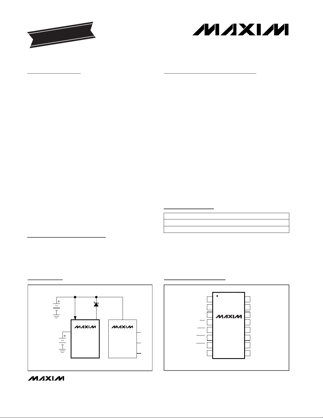
Typical Operating Circuit
19-4785; Rev 0; 11/98
PART
MAX1612EEE
MAX1613EEE
-40°C to +85°C
-40°C to +85°C
TEMP. RANGE PIN-PACKAGE
16 QSOP
16 QSOP
EVALUATION KIT MANUAL
FOLLOWS DATA SHEET
Pin Configuration
Ordering Information
For free samples & the latest literature: http://www.maxim-ic.com, or phone 1-800-998-8800.
For small orders, phone 1-800-835-8769.
MAIN BATTERY
OR
WALL
ADAPTER
AUXILIARY
BRIDGE
BATTERY
LRI
BBATT
MAX1613
APPLICATION
CIRCUIT
DC-DC
OUTPUT
V+
MAX1630MAX1612
DC-DC
CONVERTER
+3.3V
+5V
V
CPU
MAX1612/MAX1613
Bridge-Battery Backup Controllers
for Notebooks
2 _______________________________________________________________________________________
ABSOLUTE MAXIMUM RATINGS
ELECTRICAL CHARACTERISTICS
(V
LRI
= V
ISET
= 20V, CCMD = DCMD = BBON = LRO, V
BBATT
= 3V, TA= T
MIN
to T
MAX
, unless otherwise noted. Typical values are at
T
A
= +25°C.) (Note 1)
Stresses beyond those listed under “Absolute Maximum Ratings” may cause permanent damage to the device. These are stress ratings only, and functional
operation of the device at these or any other conditions beyond those indicated in the operational sections of the specifications is not implied. Exposure to
absolute maximum rating conditions for extended periods may affect device reliability.
LRI, ISET to GND....................................................-0.3V to +30V
LX to GND ..............................................................-0.3V to +14V
PGND to GND .......................................................-0.3V to +0.3V
BBATT, LRO, CCMD, DCMD, FULL, BBON,
LBO to GND ..........................................................-0.3V to +6V
CC, CD, LBI, FB to GND...........................-0.3V to (V
LRO
+ 0.3V)
FB, LBI, ISET, and BBATT Current......................................50mA
LRO Output Current ...........................................................50mA
Continuous Power Dissipation (T
A
= +70°C)
QSOP (derate 8.30mW/°C above +70°C).................... 667mW
Operating Temperature Range
MAX1612/MAX1613EEE...................................-40°C to +85°C
Storage Temperature Range.............................-65°C to +160°C
Lead Temperature (soldering, 10sec)............................ +300°C
I
SINK
= 1mA
V
LBO
= V
FULL
= 5.5V
V
BBON
≥ 2V
V
LBI
= 1.9V
MAX1613
MAX1612
V
ISET
= 28V, V
BBATT
= 0
LRO rising hysteresis = 200mV
CCMD = GND, I
ISET
= 10mA, V
BBATT
= 2V,
%loss = [(I
ISET
- I
BBATT
) / I
ISET
) · 100%
V
DCMD
= 0, R
BBON
= 1MΩ to GND
(boost converter on)
5.7V ≤ V
LRI
≤ 28V
(MAX1612)
I
ISET
= 10mA, V
CCMD
= 0, V
BBATT
= 2V
V
ISET
= 0 or 28V, V
BBATT
= 6V
CONDITIONS
LBO, FULL Output Voltage Low
V0.4
LBO, FULL Output Leakage
Current
µA1I
LBO, IFULL
nA
0.2 10
I
LBI
LBI Input Current
V
1.955 2 2.045
V
LBTH
LBI Rising Trip Voltage
V
1.76 1.8 1.84
V
LBTL
LBI Falling Trip Voltage
%
0.1 5
Charge-Switch Loss Current
V
0.5 1 1.3
Charge-Switch On Voltage
µA
-5 5
I
BBATT(LEAK
)BBATT Leakage Current
18 28
I
LRI
4V ≤ V
LRI
≤ 28V
(MAX1613)
0 ≤ I
LRO
≤ 10mA
4 28
V
5.7 28
V
LRI
Linear-Regulator Input Voltage
Range
µA
0.3 5
I
ISET(LEAK
)ISET Leakage Current
V
2.65 2.97
V
UVLO
Linear-Regulator Output
Undervoltage Lockout
Threshold
V
3.1 3.3 3.5
µA
42 58
Linear-Regulator Quiescent
Current
4.7 5.0 5.3
V
LRO
Linear-Regulator Output Voltage
UNITMIN TYP MAXSYMBOLPARAMETER
Overdrive = 100mV µs
20
t
PD
LBI Comparator Response Time
BATTERY CHARGER
LOW-BATTERY COMPARATOR
MAX1612/MAX1613
Bridge-Battery Backup Controllers
for Notebooks
_______________________________________________________________________________________
3
Typical Operating Characteristics
(Circuit of Figure 3, TA = +25°C, unless otherwise noted.)
CONDITIONS UNITMIN TYP MAXSYMBOLPARAMETER
CCMD, DCMD
V
CCMD
= 0, CC = GND
V
DCMD
= 0, CD = GND
Resets the counter
Voltage that allows a new cycle, defined as
(V
BBATT
- VLX) (see
DC-DC Converter
section)
VFB= 2.1V
R
BBON
= 100kΩ to GND
VLX= 12V
CCC= 33nF
ILX= 200mA
CCD= 3.3nF
V
0.8
V
IL
Logic Input Low Level
%
-1 1
CD to CC Current Matching
V
0.4
ISET Logic Input Low Voltage
Hz
60 75.8 95
CC
OSC
CC Oscillator Frequency
Hz
600 758 950
CD
OSC
CD Oscillator Frequency
V
1.95 2.05
V
FB
FB Trip Point
µA
4.35 5.00 5.65
CC Output Current
V2.1
BBON Logic Input Low Voltage
V
-0.2 -0.1 0.2
LX Zero Crossing Trip Threshold
nA
0.15 10
I
FB
FB Input Current
A
0.580 0.835 1.100
I
PEAK
LX Switch Current Limit
µA
0.01 10
LX Off-Leakage
Ω
0.5 1.5
R
DSON
LX On-Resistance
ELECTRICAL CHARACTERISTICS (continued)
(V
LRI
= V
ISET
= 20V, CCMD = DCMD = BBON = LRO, V
BBATT
= 3V, TA= T
MIN
to T
MAX
, unless otherwise noted. Typical values are at
T
A
= +25°C.) (Note 1)
CCMD, DCMD
V
2.2
V
IH
Logic Input High Level
V
CCMD
, V
DCMD
= 0 to V
LRO
µA
1
I
(CCMD),
I
(DCMD)
Logic Input Leakage Current
TIMER BLOCK
DC-DC CONVERTER
Note 1: Specifications from 0°C to -40°C are guaranteed by design, not production tested.
0
20
40
60
80
100
120
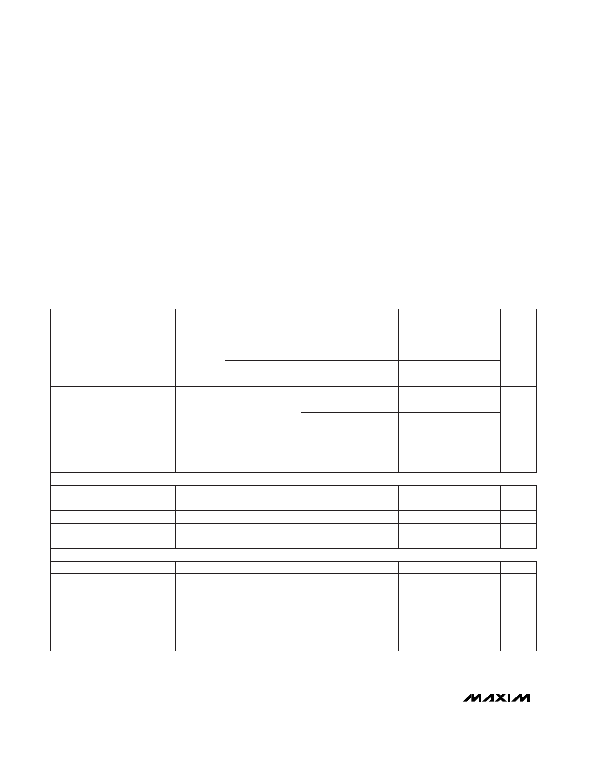
0 105 15 20 25 30 35 40 45
DISCHARGE TIME
vs. OUTPUT CURRENT
MAX612-01
OUTPUT CURRENT (mA)
DISCHARGE TIME (MINUTES)
2 CELLS (SANYO N-50AAA)
V
OUT
= 7V
V
OUT
= 5V
100k
1
0.1 10 1001 1000
OSCILLATOR FREQUENCY
vs. CAPACITANCE
10
MAX1612-02
CAPACITANCE (nF)
OSCILLATOR FREQUENCY (Hz)
100
1k
10k
CD
CC
90
80
70
0
1µ 10µ 1m 10m
100m
100µ 1
EFFICIENCY vs. OUTPUT CURRENT
(BBATT = 3.6V)
MAX612-03
OUTPUT CURRENT (A)
EFFICIENCY (%)
30
20
10
60
50
40
V
OUT
= 7V
V
OUT
= 6V
V
OUT
= 5V
BBATT = 3.6V
R
BBON
= 240kΩ
NOTE: DC-DC
CONVERTER
SUPPLIES V
LRI
MAX1612/MAX1613
Bridge-Battery Backup Controllers
for Notebooks
4 _______________________________________________________________________________________
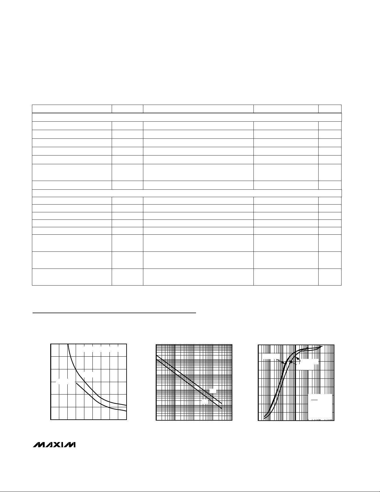
Typical Operating Characteristics (continued)
(Circuit of Figure 3, TA = +25°C, unless otherwise noted.)
90
80
70
0
1µ 10µ 1m 10m
100m
100µ 1
EFFICIENCY vs. OUTPUT CURRENT
(BBATT = 2.4V)
MAX612-04
OUTPUT CURRENT (A)
EFFICIENCY (%)
30
20
10
60
50
40
V
OUT
= 7V
V
OUT
= 6V
V
OUT
= 5V
BBATT = 2.4V
R
BBON
= 240kΩ
NOTE: DC-DC
CONVERTER
SUPPLIES V
LRI
90
80
70
0
1µ 10µ 1m 10m
100m
100µ 1
EFFICIENCY vs. OUTPUT CURRENT
(BBATT = 6V)
MAX612-05
OUTPUT CURRENT (A)
EFFICIENCY (%)
30
20
10
60
50
40
BBATT = 3.6V
BBATT = 2.4V
V
OUT
= 6V
R
BBON
= 240kΩ
NOTE: DC-DC
CONVERTER
SUPPLIES V
LRI
0
20
10
40
30
50
0 10 155 20 25 30
QUIESCENT CURRENT
vs. LRI VOLTAGE
MAX612-06
V
LRI
(V)
QUIESCENT CURRENT (µA)
MAX1612
MAX1612
MAX1613
MAX1613
R
BBON
= 100kΩ TO GND
V
BBON
= V
LRO
0
600
400
200
800
1000
1200
5 13117 9 15 17 19 21 23 25
PEAK CURRENT vs. BBON CURRENT
MAX612-07
BBON CURRENT (µA)
PEAK CURRENT (mA)
3.20
3.24
3.22
3.26
3.32
3.30
3.34
3.28
3.36
0 4 6 8 102 12 14 16 18 20
MAX1613
LRO VOLTAGE vs. LOAD CURRENT
MAX612-10
LOAD CURRENT (mA)
V
LRO
(V)
V
LRI
= 20V
-2.0
-1.0
-1.5
0
-0.5
0.5
1.0
1.5
2.0
2.0 3.0 3.52.5 4.0 4.5 5.0 5.5 6.0
BBATT LEAKAGE CURRENT
vs. BBATT INPUT VOLTAGE
MAX612-08
BBATT INPUT VOLTAGE (V)
BBATT LEAKAGE CURRENT (µA)
3.25
3.27
3.31
3.29
3.33
3.35
0 105 15 20 25 30
MAX1613
LRO VOLTAGE vs. LRI VOLTAGE
MAX612-09
V
LRI
(V)
V
LRO
(V)
I
LOAD
= 5mA
100
150
250
200
300
350
120 200160 240 280 320 360
SWITCHING FREQUENCY vs. R
BBON
MAX612-11
R
BBON
(kΩ)
SWITCHING FREQUENCY (kHz)

MAX1612/MAX1613
Bridge-Battery Backup Controllers
for Notebooks
_______________________________________________________________________________________ 5
NAME FUNCTION
1 ISET
Bridge-Battery Charge-Current Input. Connect a current-setting resistor from this input to a voltage
higher than the bridge battery. Maximum current rating is 10mA. Pulling ISET below 0.4V resets the
internal counter.
2 BBATT Bridge-Battery Connection. Bridge-battery charger output.
PIN
3 LX Step-Up DC-DC Converter N-Channel MOSFET Drain. The maximum operating range is 12V.
4
LBO
Open-Drain Low-Battery Detector Output. When V
LBI
falls below 1.8V, LBO sinks current. When
V
LBI
rises above 2.0V, LBO becomes high impedance.
8 FULL
Open-Drain Bridge-Battery Full Indicator Output. When the internal timer reaches all 1sec, FULL
goes high impedance.
7
CCMD
Charge Command Input. When low with DCMD high, the internal switch from ISET to BBATT is
closed, charging the bridge battery. CCMD is inhibited if DCMD is low. The internal timer counts up
at a frequency set by the CC capacitor.
6
DCMD
Discharge Command Input. When low with CCMD high, the internal timer counts down at a
frequency set by the CD capacitor. When both DCMD and CCMD are low, discharge takes
precedence.
5
BBON
Bridge-Battery On Input. When high, the DC-DC converter turns off. When pulled low through an
external resistor, the resistor sets the peak inductor current. The inductor current is approximately
42,000 times the current in the external resistor (R
BBON
).
13 CD
Discharge Oscillator Capacitor Input. This capacitor sets the discharging oscillator frequency,
which determines the maximum time to decrement the counter from all 1s to all 0s. Calculate the
capacitor value as follows: CD (in nF) = 4.3 · discharge time (in hours).
12 CC
Charge Oscillator Capacitor Input. This capacitor programs the charging oscillator frequency,
which sets the time for the internal counter to reach all 1s. Determine the capacitor value by: CC
(in nF) = 4.3 · charge time (in hours).
11 GND Ground
10 LBI
Low-Battery-Detector Input. When LBI falls below 1.8V, LBO goes low and sinks current. When LBI
goes above 2.0V, LBO goes high impedance. Hysteresis is typically 200mV.
9 FB
Feedback Input of Step-Up DC-DC Converter. Regulates to 2V. Connect feedback resistors to set
output voltage (Figure 2).
Pin Description
14 PGND Power Ground and Step-Up DC-DC Converter N-Channel MOSFET Source
15 LRO
5V (MAX1612) or 3.3V (MAX1613) Linear-Regulator Output. Bypass to GND with a 1µF capacitor.
Maximum external load current is 10mA.
16 LRI Linear-Regulator Supply Input

MAX1612/MAX1613
_______________Detailed Description
The MAX1612/MAX1613 manage the bridge battery
(auxiliary battery) in portable systems. These devices
consist of a timer block that monitors the charging
process, a linear regulator for supplying IC power and
external circuitry to the MAX1612/MAX1613, and a DCDC step-up converter that powers the system when the
main battery is removed (Figure 1). The boost DC-DC
converter reduces the number of bridge-battery cells
required to supply the system’s DC-DC converter.
When the main supply is present, the DC-DC converter
is inactive, reducing the drain on the main battery to
only 18µA. However, if the main battery voltage falls (as
detected by the low-battery comparator), the bridge
battery becomes the input source.
The MAX1612/MAX1613 have an internal linear regulator set at +5V (MAX1612) or +3.3V (MAX1613). The linear regulator can deliver a load up to 10mA, making it
capable of powering external components such as a
microcontroller (Figure 4). An undervoltage lockout feature disables the device when the input voltage falls
below the operating range, preventing the DC-DC converter from inadvertently powering up.
The MAX1612/MAX1613 feature an internal counter
intended to track the charging and discharging
process. The counter tracks the charge on the bridge
battery, allowing trickle charge to terminate when the
maximum charge is achieved. The charging rate is
determined by current through the ISET switch, and
limited by the switch’s maximum current specification
as well as by the bridge cell’s charging capability. As
Bridge-Battery Backup Controllers
for Notebooks
6 _______________________________________________________________________________________
N-CHANNEL
PGND
V
CHARGE
V
MAIN
R
ISET
L1
ISETLRI BBATT
V
BBATT
LX
FB
D1
R1
R2
R3
C
OUT
LBI
DISCHARGE
OSCILLATOR
TIMER BLOCK
CHARGE/DISCHARGE
COUNTER
CHARGE
OSCILLATOR
2.0V
REFERENCE
+3.3/+5V
LINEAR REGULATOR
1.8V/2.0V
BBON
R
BBON
DCMDCCMDFULL
CD
CC
C
CD
C
CC
GND
LRO
TO EXTERNAL
LOADS
LBO
TO MAIN
DC-DC
MAX1612
MAX1613
PULSE-
FREQUENCY
MODULATION
CONTROL
BLOCK
Figure 1. Functional Diagram

specifications vary, the counter frequency can be
adjusted to accommodate these variances by adjusting
CCC. Similarly, the discharging oscillator frequency can
be adjusted with the CCDcapacitor. However, the rate
of bridge battery discharge depends on the DC-DC
converter’s load. Decrementing the charge/discharge
counter is used only to estimate the remaining charge
on the bridge battery. The counter increments (or
decrements) based on CCMD and DCMD logic states.
Note that the net charge must exceed the net discharge to compensate for charging efficiency losses.
Figure 3 shows a typical stand-alone application (see
Design Procedure
for details). It reduces the need for
an external microcontroller to manage these functions.
However, if the design requires greater flexibility, a
microcontroller can be used as shown in Figure 4.
DC-DC Converter
The DC-DC step-up converter is a pulse-frequency
modulated (PFM) type. The on-time is determined by
the time it takes for the inductor current to ramp up to
the peak current limit (set via R
BBON
), which in turn is
determined by the bridge battery voltage and the
inductor value. With light load or no load, the converter
is forced to operate in discontinuous-conduction mode
(where the inductor current decays to zero with each
cycle) by a comparator that monitors the LX voltage
waveform. The converter will not start a new cycle until
the voltage at LX goes below the battery voltage. At full
load, the converter operates at the crossover point
between continuous and discontinuous mode. This
“edge of continuous” algorithm results in the minimum
possible physical size for the inductor. At light loads,
the devices pulse infrequently to maintain output regulation (VFB≥ 2V). Note that the LX comparator requires
the DC-DC output voltage to be set at least 0.6V above
the maximum bridge battery voltage.
Timer Block
The MAX1612/MAX1613 have an internal charge/discharge counter that keeps track of the bridge-battery
charging/discharging process. When CCMD is low and
DCMD is high, the internal counter increments until the
FULL pin goes high, indicating that the counter has
reached all 1s. The maximum counter value is 221.
Additional pulses from the CC oscillator will not cause
the counter to wrap around. In the stand-alone application (Figure 3), terminate the charging process automatically by connecting FULL to CCMD. In a microcontroller application, pull CCMD high. The counter
only specifies the maximum time for full charging; it
does not control the actual rate of charging. CCMD
controls the charging switch, and the resistor at ISET
sets the charging rate.
During the discharging process, drive DCMD low in
order to begin decrementing the counter. When the
counter is full, FULL is high. As soon as the counter
decrements just two counts, the FULL pin sinks current,
indicating that the battery is no longer full. The counter
only indicates the relative portion of the charge remaining. The incrementing and decrementing rate depends
on the maximum charge and discharge times set forth
by charging and discharging rates (see the following
equations for CC and CD). Note that the actual discharging is caused by the input current of the step-up
DC-DC converter loading down the bridge battery,
which is controlled via BBON rather than by DCMD.
The CC and CD capacitor values determine the
upcount and downcount rates by controlling the discharging oscillator frequency. Determine the maximum
charge and discharge times as follows:
CCC(nF) = 4.3 · t
HRS
CCD(nF) = 4.3 · t
HRS
where CCCis the charging capacitor, CCDis the discharging capacitor and t
HRS
is the maximum time in
hours for the process. Choose values that allow for
losses in the battery charging and discharging
process, such as battery charging inefficiencies, errors
in charging current value caused by variable main battery voltages, leakage currents, and losses in the
device’s internal switch. For charging, use the standard
charge rate recommended by the battery manufacturer. The maximum charging current is restricted to
the battery specifications. Consult the battery manufacturer’s specifications. Do not set the charging
current above 10mA.
MAX1612/MAX1613
Bridge-Battery Backup Controllers
for Notebooks
_______________________________________________________________________________________ 7
MICROCONTROLLER
I/O
BBON
LRO
GND
250k
1M
MAX1612
MAX1613
2N7002
Figure 2. Reducing BBON Noise Sensitivity

MAX1612/MAX1613
The counter block can be used to estimate the charge
remaining in the battery. For example, if the maximum
expected charge time is 14 hours (CCC= 60nF) and
the maximum expected discharge time is about 2 hours
(CCD= 8.6nF), the battery reaches full charge in 14
hours with the FULL pin going high. If the bridge battery must supply the load for 1 hour, the counter will
decrement down to about half full. Recharging the battery will now require only 7 hours to reach all 1s in the
counter, signaling with FULL going high.
If both DCMD and CCMD are pulled low simultaneously, the counter defaults to the discharge mode. When
the bridge battery is supplying the circuit, it is considered to be in discharge mode (Table 1).
Charge Current Selection (ISET)
A resistor between ISET and a voltage higher than the
bridge battery sets the charging rate. The switch is
open when CCMD is high and is turned on when
CCMD is pulled low (assuming DCMD is high). If the
voltage at ISET falls below 0.4V, the internal counter
resets to all 0s. The internal high-voltage switch has a
typical on-state voltage drop of 1V (Figure 1).
Therefore, the charge current equals:
I
ISET
= [ (V
CHARGE
- V
BBATT
) - 1V] / R
ISET
Linear-Regulator Output (LRO)
The linear-regulator output, LRO, is set at +5.0V for the
MAX1612 and at +3.3V for the MAX1613, with a tolerance of ±6%. For powering external circuitry such as
the microcontroller shown in Figure 4, LRO is guaranteed to deliver up to 10mA while maintaining regulation.
If the voltage at the linear-regulator input falls below the
operating range, an undervoltage-lockout feature shuts
down the entire device.
Bridge-Battery Backup Controllers
for Notebooks
8 _______________________________________________________________________________________
DCMD CCMD
COUNTER ISET SWITCH
0 0 Count Down Off
0 1 Count Down Off
1 0 Count Up On
1 1 No Count Off
Table 1. CCMD, DCMD Truth Table
MAX1612
MAX1613
LX
MAIN
BATTERY
22µH
22µF
2.2k
160k
470k
+5V/3.3V
470k
1µF
0.33µF
100µF
ALWAYS-ON
OUTPUT
BRIDGE
BATTERY
442k
SYSTEM
DC-DC
(MAX1630)
20k
200k
BBATT
MBR0530
PGND
ISET
FB
LBI
GNDCDCC
4.7nF
68nF
BBON
DCMD
LBO
CCMD
FULL
LRO
Figure 3. Stand-Alone Application

Low-Battery Comparator (LBI,
LBO
)
The MAX1612/MAX1613 feature a low-battery comparator with a factory-preset 1.8V threshold. This comparator is intended to monitor the main high-voltage
battery. As the voltage falls below 1.8V, the open-drain
LBO output sinks current. With 200mV of hysteresis, the
output will not go high until V
LBI
exceeds 2.0V. LBO
can easily be connected to BBON to start the DC-DC
converter when V
LBI
< 1.8V (stand-alone application,
Figure 3). Figure 4 shows an application using a microcontroller, where LBO alerts the microcontroller to the
falling voltage and pulls BBON low through an external
resistor to start the DC-DC converter while also pulling
DCMD low to start the counter.
BBON
Control Input
The BBON input serves two functions: setting the peak
LX switch current, and enabling the DC-DC converter.
The control signal is normally applied to R
BBON
rather
than at the pin itself. The peak LX switch current is
directly proportional to and 42,000 times greater than
the current through R
BBON
(see
Typical Operating
Characteristics
). The BBON pin is internally regulated
to 2V, so that when the control input is forced low, the
voltage across R
BBON
is 2V.
When driving BBON from external logic, ensure the low
state has minimal noise. Otherwise, drive R
BBON
with
an N-channel FET whose source is returned directly to
GND (Figure 2).
Applications Information
Design Procedure
The following section refers to the Functional Diagram
of Figure 1.
Step 1: Select the output voltage and maximum output
current for the boost DC-DC converter. Generally,
choose an output voltage high enough to run the main
system’s buck DC-DC converters. Assuming the maximum battery capacity is 50mAh (Sanyo 1.2V N-50AAA),
the following equations can help the design process:
I
PEAK
= 2 · I
OUT
· (V
OUT
+ VD) / (V
BBATT
- V
RDSON
)
IIN= 0.5 · I
PEAK
MAX1612/MAX1613
Bridge-Battery Backup Controllers
for Notebooks
_______________________________________________________________________________________ 9
MAX1612
MAX1613
LX
MAIN
BATTERY
15µH
20µF
2.4k
250k
470k 470k
47µF
1µF
BRIDGE
BATTERY
V
CC
MICROCONTROLLER
I/O
I/O
I/O
I/O
I/O
I/O
750k
SYSTEM
DC-DC
(MAX1630)
35.2k
479.1k
BBATT
MBR0530
PGND
ISET
FB
LBI
GNDCDCC
0.01µF
0.1µF
BBON
LRO
LBO
FULL
DCMD
CCMD
0.33µF
2N7002*
*OPTIONAL, TO RESET COUNTER
Figure 4. Microcontroller-Based Application

MAX1612/MAX1613
where I
PEAK
is the peak current, I
OUT
is the load cur-
rent, V
BBATT
is the bridge-battery voltage, VDis the for-
ward drop across D1, V
OUT
is the output voltage, IINis
average current provided by the bridge battery, and
V
RDS(ON)
is the voltage drop across the internal Nchannel power transistor at LX (typically 0.5V). A larger
number of cells reduces the I
PEAK
and, in effect,
reduces the discharge current, thereby extending the
discharge time. The same is true for decreasing the
output voltage or output current. For example, choose
the following values: I
OUT
= 100mA, V
OUT
= 5V, and
V
BBATT
= 2V (two cells). Using the minimum voltage of
1V for each cell, Table 2 summarizes some common
values.
Step 2: To avoid saturation, choose an inductor (L) with
a peak current rating above the I
PEAK
calculated in
Step 1. Use low series resistance (≤ 200mΩ), to optimize efficiency. In this example, a 15µH inductor is
used. See Table 4 for a list of component suppliers.
The “edge-of-continuous” DC-DC algorithm causes the
inductor value to fall out of the peak current equation.
Therefore, the exact inductor value chosen is not critical to the design. However, the switching frequency is
inversely proportional to inductance, so trade-offs of
switching losses versus physical inductor size can be
made by adjusting the inductor value.
where f is the switching frequency, V
OUT
is the output
voltage, V
RDSON
is the voltage across the internal MOS-
FET switch, VDis the forward voltage of D1, I
PEAK
is the
peak current, and V
BBATT
is the bridge battery voltage.
The maximum practical switching frequency is 400kHz.
Step 3: Choose the charging (CCC) and discharging
(CCD) timing capacitors. These capacitors set the frequency that the counter increments/decrements.
CCC(nF) = 4.3 · expected charge time (in hours)
CCD(nF) = 4.3 · expected discharge time (in hours)
For instance, using a charge time of 16 hours and a discharge time of one hour, CCC= 68nF and CCD= 4.3nF.
(Consult battery manufacturers’ specifications for standard charging information, which generally compensates for battery inefficiencies.)
Step 4: Using the peak current calculated in Step 1,
calculate the series resistor (R
BBON
) as follows:
R
BBON
= (V
BBON
· 42,000) / I
PEAK
where V
BBON
= 2V (internally regulated).
Step 5: Resistors R1, R2, and R3 set the DC-DC converter’s output voltage and the low-battery comparator
trip value. The sum of R1, R2, and R3 must be less than
2MΩ, to minimize leakage errors. Choose resistor R1 =
750kΩ for the example. Calculate R2 and R3 as follows:
R2 = [ V
OUT
(R3) - 2 (R1) - 2 (R3) ] / (2 - V
OUT
)
R3 = (R1 + R2) / [ (V
TRIP
/ 1.8) - 1]
Bridge-Battery Backup Controllers
for Notebooks
10 ______________________________________________________________________________________
V
OUT
(V)
V
BBATT
(V)
AVERAGE
I
PEAK
(mA)
I
IN
(mA)
MINIMUM
DISCHARGE TIME
(MINUTES)
6 4 300 150 20
6 2 600 300 10
5 2 500 250 12
4.5 2 450 225 13.2
6 3 400 200 15
5 3 333 167 18
4.5 3 300 150 20
5 4 250 125 24
Table 2. Summary of Common Values for
Designing with the MAX1612/MAX1613
Note:
In this table, I
OUT
= 100mA and battery capacity = 50mAh.
Table 3. Component List
INDUCTORS CAPACITORS RECTIFIERS BATTERY
Sumida CD43
or CD54 series
Sprague 595D
series, AVX
TPS series
Motorola
MBR0530,
NIEC
EC10QS03L
Sanyo
N-50AAA
SUPPLIER PHONE FAX
AVX USA: 207-287-5111 USA: 207-283-1941
Motorola
USA: 408-749-0510
800-521-6274
—
NIEC
USA: 805-867-2555
Japan: 81-3-3494-7411
USA: 805-867-2556
Japan: 81-3-3494-7414
Sumida
USA: 708-956-0666
Japan: 81-3-3607-5111
USA: 708-956-0702
Japan: 81-3-3607-5144
Table 4. Component Suppliers
Sanyo
USA: 619-661-6835
Japan: 81-7-2070-6306
USA: 619-661-1055
Japan: 81-7-2070-1174
f
=
L(I )
(V V ) (V V V )
1
PEAK
− − −
BBATT RDSON OUT BBATT D
(V V V )
− −
OUT RDSON D

where V
OUT
is the DC-DC converter’s output voltage
and V
TRIP
is the voltage level the main battery must fall
below to trip the low-battery comparator. For example,
for a +5V boost DC-DC output, a 4.75V main battery
trip level is feasible. For this case, R1 = 750kΩ, R2 =
26kΩ, and R3 = 474kΩ.
Step 6: Select a resistor value to set the charging current. The resistor value at ISET limits the current
through the switch for bridge-battery charging. There is
a voltage drop across the high-voltage switch (see
Electrical Characteristics
) with a typical value of 1V.
The maximum charge current through the internal highvoltage switch is 10mA.
R
ISET
= (V
CHARGE
- V
SWITCH
- V
BBATT
) / I
CHARGE
where V
CHARGE
is the charging supply voltage,
V
SWITCH
is the drop across the high-voltage internal
switch, V
BBATT
is the bridge battery voltage, and
I
CHARGE
is the charge current (in amperes).
Stand-Alone Application
To reduce cost and save space, the MAX1612/
MAX1613 can be operated in a stand-alone configuration, which eliminates the need for a microcontroller. A
stand-alone configuration could also reduce the workload of an existing microcontroller in the system, thus
allowing these unused I/Os to be used for other applications.
Figure 3 shows the MAX1612/MAX1613 operating without the microcontroller by using the low-battery detector to monitor the main battery. If the main battery is too
low, LBO pulls BBON and DCMD low to start the DCDC step-up converter and allow the bridge battery to
discharge. If the bridge battery requires charging,
FULL pulls CCMD low to start the battery charging
process. If both CCMD and DCMD are low, discharging takes precedence and the bridge battery keeps the
boost DC-DC converter active.
Microcontroller-Based Application
The MAX1612/MAX1613 are also suited to operate in a
microcontroller-based system. A microcontroller-based
application provides more flexibility by allowing for separate, independent control of the charging process, the
DC-DC converter, and the counter. Independent control can be beneficial in situations where other subsystems are operating, so that automatic switchover of
power might create some timing issues. If necessary, a
microcontroller can be used to reset the counter by taking ISET low. Another advantage of a microcontrollerbased system is the ability to stop charging the bridge
battery during a fault condition.
Figure 4 shows an example of how the MAX1612/
MAX1613 can be interfaced to a MAX1630 to deliver
the input voltage to the main DC-DC converter. In this
example, the microcontroller monitors the main battery’s status and switches over to the bridge battery
when V
MAIN
falls below a specified trip level (see
Design Procedure
). When V
MAIN
falls below the LBI
threshold, LBO goes low. This signals the microcontroller, via an I/O, to switch over to the bridge battery as
the input source to the system main DC-DC converter.
In this application, the microcontroller also initiates the
bridge-battery charging process. When CCMD goes
low with DCMD high, the battery is charged through the
internal switch. The counter increments until it overflows
and FULL goes high, indicating a full charge. The
microcontroller I/O can read and write the appropriate
states to control the execution and timing of the entire
process.
If the main DC-DC is supplied by the main source, the
MAX1612/MAX1613’s step-up converter turns off, minimizing power consumption. The device typically draws
only 18µA of quiescent current under this condition.
MAX1612/MAX1613
Bridge-Battery Backup Controllers
for Notebooks
______________________________________________________________________________________ 11
Table 5. Surface-Mount Inductor Information
MANUFACTURER
AND PART
INDUCTANCE
(µH)
RESISTANCE
(Ω)
RATED CURRENT
(A)
HEIGHT
(mm)
Sumida CD54-100 10 0.100 1.44 4.5
Sumida CD43-8R2 8.2 0.132 1.26 3.2
Sumida CD43-150 15 0.235 0.92 3.2
Sumida CD54-150 15 0.140 1.30 4.5
Sumida CD54-220 22 0.180 1.11 4.5

MAX1612/MAX1613
Bridge-Battery Backup Controllers
for Notebooks
12 ______________________________________________________________________________________
Package Information
TRANSISTOR COUNT: 3543
Chip Information
QSOP.EPS
 Loading...