

General Description
The MAX1608/MAX1609 provide remote input/output (I/O)
expansion through an SMBus™ 2-wire serial interface.
Each device has eight high-voltage open-drain outputs
that double as TTL-level logic inputs, providing continuous
bidirectional capabilities. The open-drain outputs tailor the
MAX1608/MAX1609 for use in load-switching and other
level-shifting applications as well as general-purpose I/O
applications.
Two complete sets of registers allow the device and its
outputs to be toggled between two states using the
SMBSUS input, without the inherent latency of reprogramming outputs over the serial bus. The eight I/O lines are
continuously monitored and can be used as inputs. Each
line can generate asynchronous maskable interrupts on
the falling edge, the rising edge, or both edges.
For load-switching applications, the MAX1608 is designed
to drive N-channel MOSFETs, and its outputs are low
upon power-up; the MAX1609 is designed to drive Pchannel MOSFETs, and its I/Os are high impedance upon
power-up. Other features of both devices include thermaloverload and output-overcurrent protection, ultra-low supply current, and a wide +2.7V to +5.5V supply range. The
MAX1608/MAX1609 are available in space-saving 16-pin
QSOP packages.
Applications
Parallel I/O Expansion
Power-Plane Switching
Notebook and Desktop Computers
Servers and Workstations
Notebook Docking Stations
Industrial Equipment
Features
♦ Serial-to-Parallel or Parallel-to-Serial Conversions
♦ 8 General-Purpose Digital I/O Pins
(withstand +28V)
♦ SMBus 2-Wire Serial Interface
♦ Supports SMBSUS Asynchronous Suspend
♦ 9 Pin-Selectable Slave Addresses
♦ Outputs High Impedance on Power-Up (MAX1609)
♦ Outputs Low on Power-Up (MAX1608)
♦ 2.5µA Supply Current
♦ +2.7V to +5.5V Supply Range
♦ 16-Pin QSOP Package
MAX1608/MAX1609
Octal SMBus-to-Parallel I/O Expanders
________________________________________________________________ Maxim Integrated Products 1
19-1639; Rev 0; 1/00
PART
MAX1608EEE
MAX1609EEE
-40°C to +85°C
-40°C to +85°C
TEMP. RANGE PIN-PACKAGE
16 QSOP
16 QSOP
Ordering Information
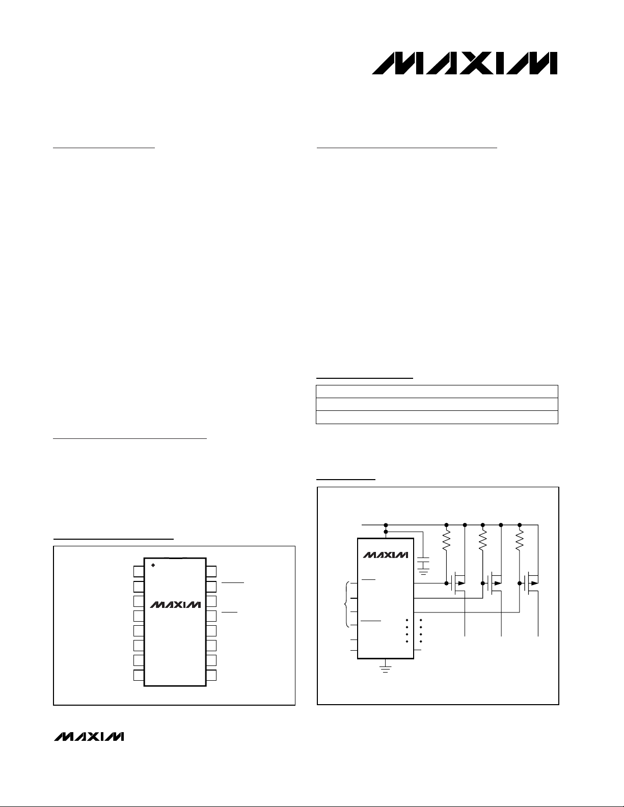
Typical Operating Circuits
Typical Operating Circuits continued at end of data sheet.
16
15
14
13
12
11
10
9
1
2
3
4
5
6
7
8
IO0 V+
SMBSUS
SMBCLK
ALERT
SMBDATA
ADD1
ADD0
GND
TOP VIEW
MAX1608
MAX1609
QSOP
IO1
IO2
IO5
IO3
IO4
IO6
IO7
Pin Configuration
SMBus is a trademark of Intel Corp.
For free samples and the latest literature, visit www.maxim-ic.com or phone 1-800-998-8800.
For small orders, phone 1-800-835-8769.
+2.7V TO +5.5V
V+
MAX1609
100k
0.1µF
100k 100k
P-CH
GND
IO1
IO2
IO3
LOAD1 LOAD2 LOAD3
IO7
TO/
ALERT
SMBDATA
SMBCLK
SMBSUS
ADD1
ADD
SMBUS
FROM
HOST
MAX1608/MAX1609
Octal SMBus-to-Parallel I/O Expanders
2 _______________________________________________________________________________________
ABSOLUTE MAXIMUM RATINGS
ELECTRICAL CHARACTERISTICS
(V+ = +2.7V to +5.5V, TA= -40°C to +85°C, unless otherwise noted. Typical values are at TA= +25°C.) (Note 1)
Stresses beyond those listed under “Absolute Maximum Ratings” may cause permanent damage to the device. These are stress ratings only, and functional
operation of the device at these or any other conditions beyond those indicated in the operational sections of the specifications is not implied. Exposure to
absolute maximum rating conditions for extended periods may affect device reliability.
V+ to GND ................................................................-0.3V to +6V
IO_ to GND .............................................................-0.3V to +30V
IO_ Sink Current..................................................-1mA to +50mA
SMBCLK, SMBDATA, SMBSUS
and ALERT to GND .............................................-0.3V to +6V
ADD_ to GND ...............................................-0.3V to (V+ + 0.3V)
SMBDATA and ALERT Sink Current...................-1mA to +50mA
Continuous Power Dissipation (T
A
= +70°C)
16-Pin QSOP (derate 8.3mW/°C above +70°C)...........667mW
Operating Temperature Range ...........................-40°C to +85°C
Storage Temperature Range .............................-65°C to +150°C
Lead Temperature (soldering, 10s) .................................+300°C
10°C typical hysteresis
ALERT forced to 5.5V
Static, all IOs low or pulled to 0
ALERT forced to 0.4V
SMBDATA forced to 0.6V
Static, outputs in any combination of on or off
states up to 28V
IO_, SMBSUS, SMBCLK, SMBDATA
IO_, SMBSUS, SMBCLK, SMBDATA
SMBSUS, SMBCLK, SMBDATA (Note 2)
(Note 3)
IO_ forced to 28V
10% or 90% of I/O to 10% of SMBCLK (Note 3)
IO_ to ALERT
IO_, V+ = 4.5V
IO_ forced to 1.0V, V+ = 4.5V
SMBus interface operating,
clock frequency = 100kHz
Falling edge of V+
SMBSUS to IO_
IO_ forced to 0.4V
SMBCLK to IO_
CONDITIONS
°C
140
Thermal Shutdown
µA
1
ALERT Output High Leakage Current
mA
1
ALERT Output Low Sink Current
mA
6
SMBus Output Low Sink Current
V
0.8
Logic Input Low Voltage
V
2.1
Logic Input High Voltage
V
0 5.5
SMBus Logic Input Voltage Range
µs
3
IO_ Data Hold Time
µs
10
IO_ Data Set-Up Time
10
1
µs
2.5
Propagation Delay
3.5 9
µA
718
V
2.7 5.5
Supply Voltage Range
Supply Current (Note 2)
µA
0.5 2
I/O Leakage Current
mA
15 25 50
I/O Current Limit
813
7
V
1.2 1.8 2.5
POR Threshold Voltage
mA
2
I/O Sink Current
UNITSMIN TYP MAXPARAMETER
SMBCLK, SMBDATA
SMBDATA, SMBCLK, SMBUS, ADD_
ADD_ during address sampling (POR, SPOR,
and RAP) to V+ and GND (Note 4)
pF
5
SMBus Input Capacitance
µA
-1 1
Logic Input Current
kΩ
20
Sample Address Input Impedance
MAX1608/MAX1609
Octal SMBus-to-Parallel I/O Expanders
_______________________________________________________________________________________ 3
TIMING CHARACTERISTICS
(V+ = +2.7V to +5.5V, TA= -40°C to +85°C, unless otherwise noted. Typical values are at TA= +25°C.) (Note 1)
Note 1: Specifications from 0°C to -40°C are guaranteed by design, not production tested.
Note 2: For supply current, SMBus logic inputs driven to 0 or V+.
Note 3: Data hold and set-up times measured from falling edge of 9th clock.
Note 4: Must be driven to GND, V+, or floating. See SMBus Addressing section.
Note 5: The SMBus logic block is a static design and will work with clock frequencies down to DC. While slow operation is possible,
it violates the 10kHz minimum clock frequency and SMBus specifications and may use excessive space on the bus.
90% to 90% points
10% to 10% points
(Note 5)
10% or 90% of SMBDATA to 10% of SMBCLK
90% of SMBCLK to 10% of SMBDATA
10% of SMBDATA to 90% of SMBCLK
SMBCLK, SMBDATA; 10% to 90% points
SMBCLK, SMBDATA; 90% to 10% points
90% to 90% points
Master clocking in data
CONDITIONS
µs
3
SMBCLK Falling Edge to
SMBDATA Valid Time
µs
4
t
HIGH
SMBCLK Clock High Time
µs
4.7
t
LOW
kHz
DC 100
SMBus Clock Frequency
SMBCLK Clock Low Time
ns
300
t
HD:DAT
SMBus Data Hold Time
ns
250
t
SU:DAT
SMBus Data Valid to SMBCLK
Rising Edge Time
µs
4
t
SU:STO
SMBus Stop-Condition Setup
Time
µs
4
t
HD:STA
SMBus Start-Condition Hold
Time
µs
1
SMBus Rise Time
ns
300
SMBus Fall Time
µs
4.7
SMBus Start-Condition
Setup Time
ns
500
t
SU:STA
SMBus Repeated StartCondition Setup Time
UNITSMIN TYP MAXSYMBOLPARAMETER
0
5.0
2.5
10.0
7.5
12.5
15.0
2.5 3.5 4.03.0 4.5 5.0 5.5
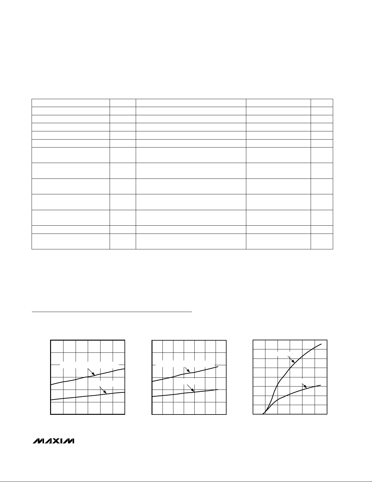
SUPPLY CURRENT vs. SUPPLY VOLTAGE
MAX1608/9 tTOC01
SUPPLY VOLTAGE (V)
SUPPLY CURRENT (µA)
IOs = 1111 1111 PULLED UP TO +28V
IOs = 0000 0000
0
5.0
2.5
10.0
7.5
12.5
15.0
-40 20 40-20 0 60 80 100
SUPPLY CURRENT vs. TEMPERATURE
MAX1608/9 TOC02
TEMPERATURE (°C)
SUPPLY CURRENT (µA)
IOs = 1111 1111 PULLED UP TO +28V
IOs = 0000 0000
0
2
4
6
8
10
12
14
16
021 3456
IO_ SINK CURRENT
vs. SUPPLY VOLTAGE
MAX1608/9 TOC03
SUPPLY VOLTAGE (V)
SINK CURRENT (mA)
V
IO_
= 1.0V
V
IO_
= 0.4V
Typical Operating Characteristics
(V+ = +5V, TA= +25°C, unless otherwise noted.)
MAX1608/MAX1609
Octal SMBus-to-Parallel I/O Expanders
4 _______________________________________________________________________________________
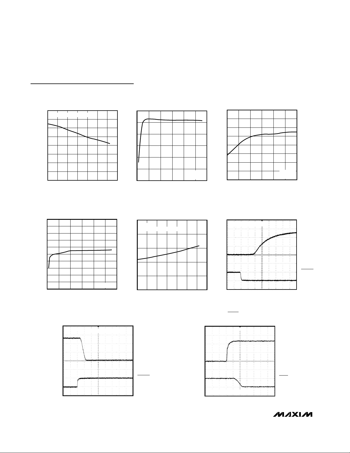
Typical Operating Characteristics (continued)
(V+ = +5V, TA= +25°C, unless otherwise noted.)
IO_
2V/div
ALERT
5V/div
MAX1608/9 TOC011
40ns/div
IO_ DRIVEN EXTERNALLY
ALERT DELAY
(IO_ RISING)
0
10
5
20
15
35
30
25
40
-40 0-20 20 40 60 80 100
IO_ CURRENT LIMIT vs. TEMPERATURE
MAX1608/9 TOC04
TEMPERATURE (°C)
IO_ CURRENT LIMIT (mA)
IO_ = 0 PULLED UP TO +28V
0
10
5
20
15
25
30
010155 202530
IO_ CURRENT LIMIT vs. IO_ VOLTAGE
MAX1608/9 TOC05
V
IO_
(V)
IO_ CURRENT LIMIT (mA)
V+ = 4.5V
IO_ = 0
0
5
10
15
20
25
30
35
40
2.5 3.53.0 4.0 4.5 5.0 5.5
IO_ CURRENT LIMIT vs. SUPPLY VOLTAGE
MAX1608/9 TOC06
SUPPLY VOLTAGE (V)
IO_ CURRENT LIMIT (mA)
V
IO_
= 15V
IO_ = 0
0
0.3
0.2
0.1
0.4
0.5
0.6
0.7
0.8
0.9
1.0
0105 15202530
IO_ BIAS CURRENT vs. IO_ VOLTAGE
MAX1608/9 TOC07
V
IO_
(V)
IO_ BIAS CURRENT (µA)
IO_ = 1
0
0.2
0.6
0.4
0.8
1.0
-40 0-20 20 40 60 80 100
IO_ BIAS CURRENT vs. TEMPERATURE
MAX1608/9 TOC08
TEMPERATURE (°C)
IO_ BIAS CURRENT (µA)
V+ = 5V
IO_ = 1 PULLED UP TO 28V
IO_
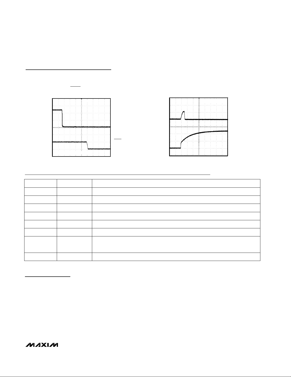
10V/div
SMBSUS
5V/div
SUSPEND-STATE DELAY
(IO_ RISING)
MAX1608/9 TOC09
100ns/div
PULL-UP = 10kΩ to 28V
IO_
10V/div
SMBSUS
5V/div
MAX1608/9 TOC010
100ns/div
SUSPEND-STATE DELAY
(IO_ FALLING)
PULL-UP = 10kΩ to 28V
MAX1608/MAX1609
Octal SMBus-to-Parallel I/O Expanders
_______________________________________________________________________________________ 5
Typical Operating Characteristics (continued)
(V+ = +5V, TA= +25°C, unless otherwise noted.)
IO_
2V/div
ALERT
5V/div
MAX1608/9 TOC012
200ns/div
IO_ DRIVEN EXTERNALLY
ALERT DELAY
(IO_ FALLING)
NAME FUNCTION
1–8 IO0 –IO7 Combined Input/Output. Open-drain output. Can withstand +28V.
9 GND Ground
PIN
10, 11 ADD0, ADD1 SMBus Address Select. See Table 1.
12 SMBDATA SMBus Serial-Data Input/Output. Open-drain output. Requires external pull-up resistor.
16 V+ Supply Voltage Input, +2.7V to +5.5V. Bypass to GND with a 0.1µF capacitor.
15
SMBSUS
SMBus Suspend-Mode Control Input. The device will enter the state previously stored in
the suspend-mode registers if low, or enter the state previously stored in the normal-mode
registers if high.
14 SMBCLK SMBus Serial Clock Input
13
ALERT
Active-Low Interrupt Output. Open-drain output. Requires external pull-up resistor.
Pin Description
Detailed Description
The MAX1608/MAX1609 convert 2-wire SMBus serial
data into eight latched parallel outputs (IO0–IO7). These
devices are intended for general-purpose remote I/O
expansion. Each device has eight high-voltage opendrain outputs that double as TTL-level logic inputs.
Typical applications range from high-side MOSFET loadswitch drivers in power-management systems, to pushbutton switch monitors, to general-purpose digital I/Os.
The MAX1608/MAX1609 include two complete sets of
registers, each consisting of one output data register to
set the output states and two interrupt mask registers.
The SMBSUS line selects which set of registers control
the device state. The input register is used to perform
readback of the actual IO states.
The MAX1608/MAX1609 operate from a single +2.7V
to +5.5V supply with a typical quiescent current of
2.5µA, making them ideal for portable applications.
Additionally, the devices include an ALERT function to
alert the master of change of condition (Figure 1).
IO_ POWER-UP RESPONSE
MAX1608
PULL-UP = 10kΩ to V+
MAX1608/9 TOC013
V
IO_
500mV/div
V+
2V/div

MAX1608/MAX1609
Octal SMBus-to-Parallel I/O Expanders
6 _______________________________________________________________________________________
Figure 1. Functional Diagram
SMBCLK
SMBDATA
ADD0
ADD1
ALERT
SMB
8
ADDRESS
DECODER
7
ALERT
RESPONSE
REGISTER
R
FAULT
LATCH
S
8
COMMAND
DECODER
INPUT
REGISTER
NORMAL RISING
INTERRUPT
MASK REGISTER
SUSPEND RISING
INTERRUPT
MASK REGISTER
NORMAL FALLING
INTERRUPT
MASK REGISTER
SUSPEND FALLING
INTERRUPT
MASK REGISTER
NORMAL
OUTPUT
REGISTER
8
8
8
TRANSITION
DETECTORS
8
IO1
IO2
IO7
1
1
THERMAL
SHUTDOWN
SUSPEND
OUTPUT
REGISTER
8
SMBSUS
1

MAX1608/MAX1609
Octal SMBus-to-Parallel I/O Expanders
_______________________________________________________________________________________ 7
SMBus Interface Operation
The SMBus serial interface is a 2-wire interface with
multi-mastering capability. The MAX1608/MAX1609 are
2-wire slave-only devices and employ standard SMBus
write-byte, send-byte, read-byte, and receive-byte
protocols (Figure 2) as documented in “System
Management Bus Specification v1.08” (available at
www.sbs-forum.org). SMBDATA and SMBCLK are
Schmitt-triggered inputs that can accommodate slower
edges; however, the rising and falling edges should still
be faster than 1µs and 300ns, respectively.
Communication starts with the master signaling the
beginning of a transmission with a START condition,
which is a high-to-low transition on SMBDATA while
SMBCLK is high. When the master has finished communicating with the slave, it issues a STOP condition,
which is a low-to-high transition on SMBDATA while
SMBCLK is high (Figures 3 and 4). The bus is then free
for another transmission from any master on the bus.
The address byte, command byte, and data byte are
transmitted between the START and STOP conditions.
Figures 3 and 4 show the timing diagrams for signals
on the 2-wire interface. The SMBDATA state is allowed
to change only while SMBCLK is low, except for the
START and STOP conditions. Data is transmitted in 8bit words and is sampled on the rising edge of SMBCLK. Nine clock cycles are required to transfer each
byte in or out of the MAX1608/MAX1609 (Figure 2),
since either the master or the slave acknowledges
receipt of the correct byte during the ninth clock. The
IC responds to the address selected by the ADD0 and
ADD1 pins (Table 1).
If the MAX1608/MAX1609 receive the correct slave
address followed by RW = 0, the selected device
expects to receive one or two bytes of information. If
the device detects a START or STOP condition prior to
clocking in a full additional byte of data, it considers
this an error condition and disregards all of the data. If
no error occurs, the registers are updated immediately
after the falling edge of the acknowledge clock pulse
(Figure 5). If the MAX1608/MAX1609 receive the correct slave address followed by RW = 1, the selected
device expects to clock out the contents of the previously accessed register during the next byte transfer.
A third interface line (SMBSUS) is used to execute commands asynchronously from previously stored registers
(see
SMBSUS
(Suspend-Mode) Input section).
SMBus Addressing
After the START condition, the master transmits a 7-bit
address followed by the RW bit (Figure 2). If the
MAX1608/MAX1609 recognizes its own address, it
sends an acknowledgment pulse by pulling SMBDATA
low.
Each slave responds to only two addresses: its own
unique address (set by ADD1 and ADD0, Table 1), and
the alert response address (0x19). The device’s unique
address is determined at power-up, with a software
sample-address-pin command (SAP), or a software
power-on-reset command (SPOR). The MAX1608/
MAX1609 address pins (ADD1–ADD0) are high impedance except when ADD1–ADD0 are sampled, which
occurs during power-up and when requested (SPOR,
RAP). During sampling, the equivalent input circuit can
be described as a resistor-divider from V+ to GND
(20kΩ each), which momentarily bias the pins to midsupply if they are left floating. To set the ADD_ pins
high or low, connect or drive the pins to the rails (V+ or
GND) to guarantee a correct level detection. During
sampling, the pins draw a momentary input bias current (V+ / 20kΩ). Also, stray capacitance in excess of
50pF on the ADD_ pins when floating may cause
address recognition problems.
SMBus Commands
The 8-bit command byte (Table 2) is the master index
that points to the registers within the MAX1608/MAX1609.
The devices include ten registers: the data registers
(NDR1–NDR3, SDR1–SDR3) are accessed through
both the read-byte and write-byte protocols (Figure 2),
the RSB and MDIF registers are accessed with the
read-byte protocols, and the RAP and SPOR registers
GND 0010 100
GND V+ 0010 110
High-Z GND 1100 100
GND
High-Z High-Z 1100 101
High-Z V+ 1100 110
V+ V+ 0111 010
ADD1
ADDRESS (A6–A0)
ADD0
V+ High-Z 0111 001
V+ GND 0111 000
High-Z 0010 101GND
MAX1608 MAX1609
0110 010
0100 100
0100 110
1101 100
1101 101
1101 110
0110 001
0110 000
0100 101
Table 1. Slave Addresses

MAX1608/MAX1609
use the send-byte protocol. The shorter receive-byte
protocol can be used instead of the read-byte protocol,
provided the correct data register was previously
selected by a read-byte or write-byte instruction. Use
caution with the shorter protocols in multimaster systems, since a second master could overwrite the command byte without informing the first master. The
register selected at POR is 0b0000 0000 so that a
receive-byte transmission that occurs immediately after
initial power-up returns the setting of NDR1. SPOR
does not reset the register pointer.
Data Registers
The MAX1608/MAX1609 each have seven data registers, three normal registers, three suspend registers,
and one readback register. The SMBUS line determines which registers controls the output states and
the interrupt mask states (normal registers if SUSBUS =
1, suspend registers if SMBSUS = 0).
Registers 1 (NDR1 and SDR1) set the state of each of
the eight outputs to either low or high impedance.
When using an external pull-up, high impedance corresponds to an output high. To use the IO_ pins as TTL
inputs only, set the corresponding bit high. The
MAX1608 powers up with all IO_ pins set low; the
MAX1609 powers up with all IO_ pins set to high
impedance (Table 3).
Register 2 (NDR2 and SDR2) are used to mask risingedge triggered interrupts, while Register 3 are used to
mask falling-edge triggered interrupts. On power-up, all
interrupts are masked (Tables 4 and 5).
The IO_ Status Data Register (RSB, Table 6) reads the
actual TTL-logic level of the IO_ pins. The IO_ pins are
sampled on the falling edge of the third byte’s acknowledge (ACK) for a read-byte format, or on the falling
edge of the first byte’s ACK for a receive-byte protocol
(Figure 5). There is a 15µs data-setup time requirement, due to the slow level translators needed for highvoltage (28V) operation. Data-hold time is 300ns. Do
not write to the RSB register because writes to readonly registers are redirected to NDR1. SMBus sends
Octal SMBus-to-Parallel I/O Expanders
8 _______________________________________________________________________________________
1b
ACK
1b7 bits
ADDRESS ACK
1b
WR
8 bits
DATA
1b
ACK P
8 bits
S COMMAND
Write-Byte Format
Receive-Byte Format
Slave Address Command Byte: selects
which register you are
writing to
Data Byte: data goes into the register
set by the command byte
1b
ACK
1b7 bits
ADDRESS ACK
1b
WR S
1b
ACK
8 bits
DATA
7 bits
ADDRESS1bRD
1b8 bits
/// PS COMMAND
Slave Address
Slave Address
Command Byte: sends command
with no data; usually used for oneshot command
Command Byte: selects
which register you are
reading from
Slave Address: repeated
due to change in dataflow direction
Data Byte: reads from
the register set by the
command byte
1b
ACK
7 bits
ADDRESS1bRD
8 bits
DATA
1b
/// PS
Data Byte: reads data from
the register commanded
by the last read-byte or
write-byte transmission;
also used for SMBus Alert
Response return address
S = Start condition Shaded = Slave transmission WR = Write = 0
P = Stop condition Ack= Acknowledged = 0 RD = Read =1
/// = Not acknowledged = 1
Figure 2. SMBus Protocols
1b
ACK
7 bits
ADDRESS1bWR
8 bits
COMMAND1bACK PS
Send-Byte Format
Read-Byte Format

data MSB first; therefore, IO7, MASK7, and data 7 bit
correspond to the MSB (first bit of the data byte).
Other Registers
RAP uses the send-byte protocol to resample the
address pins. Do not use read- and write-byte protocols to RAP because data is redirected to NDR1
although the ADD_ pins will be sampled.
SPOR uses the send-byte protocol to resample the
address pins and reset the registers to the POR state.
Do not use read- and write-byte protocols to SPOR
because data is redirected to NDR1 although the function will be performed.
MFID uses the read-byte protocol to access the ID register. Do not use write-byte protocol to MFID because
data is redirected to NDR1.
SMBSUS
(Suspend-Mode) Input
The state of the SMBSUS input selects which register
contents (NDR1 or SDR1) are applied to the IO_ pins
and which set of registers are used to mask the interrupts (NDR2, NDR3 or NDR2, SDR3). Driving SMBSUS
low selects the suspend-mode registers, while driving
SMBSUS high selects the normal registers. This feature
allows the system to select between two different I/O
MAX1608/MAX1609
Octal SMBus-to-Parallel I/O Expanders
_______________________________________________________________________________________ 9
SMBCLK
Figure 3. SMBus Write Timing
Figure 4. SMBus Read Timing
SMBDATA
AB CDEFG HIJ
t
LOWtHIGH
t
t
SU:STA
HD:STA
t
SU:DAT
t
HD:DAT
t
HD:DAT
K
t
SU:STO
M
L
t
BUF
A = START CONDITION
B = MSB OF ADDRESS CLOCKED INTO SLAVE
C = LSB OF ADDRESS CLOCKED INTO SLAVE
D = R/W BIT CLOCKED INTO SLAVE
E = SLAVE PULLS SMBDATA LINE LOW
AB CDEFG H
t
LOW
SMBCLK
SMBDATA
t
SU:STAtHD:STA
A = START CONDITION
B = MSB OF ADDRESS CLOCKED INTO SLAVE
C = LSB OF ADDRESS CLOCKED INTO SLAVE
D = R/W BIT CLOCKED INTO SLAVE
t
HIGH
F = ACKNOWLEDGE BIT CLOCKED INTO MASTER
G = MSB OF DATA CLOCKED INTO SLAVE
H = LSB OF DATA CLOCKED INTO SLAVE
I = SLAVE PULLS SMBDATA LINE LOW
t
SU:DAT
E = SLAVE PULLS SMBDATA LINE LOW
F = ACKNOWLEDGE BIT CLOCKED INTO MASTER
G = MSB OF DATA CLOCKED INTO MASTER
H = LSB OF DATA CLOCKED INTO MASTER
t
HD:DAT
J = ACKNOWLEDGE CLOCKED INTO MASTER
K = ACKNOWLEDGE CLOCK PULSE
L = STOP CONDITION, DATA EXECUTED BY SLAVE
M = NEW START CONDITION
t
SU:STO
J
K
t
BUF
I
t
SU:DAT
I = ACKNOWLEDGE CLOCK PULSE
J = STOP CONDITION
K = NEW START CONDITION

MAX1608/MAX1609
configurations asynchronously, eliminating latencies
introduced by the serial bus.
ALERT
The MAX1608/MAX1609 can generate hardware interrupts whenever the logic states of the IO_ pins change
or when thermal shutdown occurs. Interrupts are signaled on the ALERT pin. The IO_ interrupts can be
masked individually through the mask registers.
Registers NDR2 and SDR2 mask the IO_ rising-edge
interrupts, while NDR3 and SDR3 mask the IO_ fallingedge interrupts. The power-on-reset state masks all
interrupts (Tables 4 and 5).
The thermal-shutdown protection also generates an
interrupt. This interrupt cannot be masked (see Thermal
Shutdown section). An interrupt can be cleared with a
SPOR or an Alert Response. However, after an interrupt
has occurred, masking will not clear it.
Alert Response Address (0b00011001)
The alert response (interrupt pointer) address provides
quick fault identification for simple slave devices that
cannot initiate communication as a bus master. When a
slave device generates an interrupt, the host (bus master) interrogates the bus slave devices through a special
receive-byte operation that includes the alert response
address (0x19). The offending slave device returns its
own address during this receive-byte operation.
The interrupt pointer address can activate several different slave devices simultaneously. If more than one
Octal SMBus-to-Parallel I/O Expanders
10 ______________________________________________________________________________________
Figure 5. Registers/IO_ Update Timing Diagram
NDR2 01h 1111 1111
NDR3 02h 1111 1111
SDR1 03h 0000 0000
SDR2 04h 1111 1111
RAP 07h —
COMMAND
POR STATE
REGISTER
RSB 06h —
SDR3 05h 1111 1111
00h 0000 0000NDR1
08h
MAX1608
—
MAX1609
—
1111 1111
1111 1111
1111 1111
1111 1111
SPOR
—
1111 1111
1111 1111
Sample the address pins.
Normal Data Register 2. Masks the L/H interrupt.
Normal Data Register 3. Masks the H/L interrupt.
Suspend Data Register 1. Sets the IO_ states.
Suspend Data Register 2. Masks the L/H interrupt.
IO_ Status Data Register. Read pin state.
Suspend Data Register 3. Masks the H/L interrupt.
Normal Data Register 1. Sets the IO_ states.
FUNCTION
FEh 4DhMFID
—
4Dh
Execute software POR and samples address pins.
Read manufacturer ID (ASCII code for "M"axim).
Table 2. Command-Byte/Register Assignment
LAST BIT
CLOCKED
INTO SLAVE**
SCL
SDA
IO_
*NDR#, SDR# ARE LOADED. RAP, SPOR ARE INITIATED. RSB IS SAMPLED.
**DURING A RECEIVE-BYTE PROTOCOL, CORRESPONDS TO THE R/W BIT. DURING A
READ/WRITE-BYTE PROTOCOL, CORRESPONDS TO LAST BIT OF DATA.
ACKNOWLEDGE
BIT CLOCKED
INTO MASTER
t
DH:DAT
SLAVE PULLING
SDA LOW
REGISTERS
UPDATED*
t
DH:DAT
t
SCL:IO
STOP
IO_TRANSITION

slave attempts to respond, bus arbitration rules apply,
with the lowest address code going first. The other
device(s) will not generate an acknowledge and will
continue to hold the ALERT pin low until it is allowed to
clear its own interrupt.
Clearing the interrupt has no effect on the state of the
status registers.
Input/Output Pins
Each IO_ pin is protected by an internal 20mA (typical)
current-limit circuit. Typical pull-down on-resistance at
V
CC
= +2.7V and +5.5V is 100Ω and 66Ω, respectively.
When the IO_ is high impedance, it actually has a
0.5µA pull-down current source included as part of the
read-back functionality.
External pull-up resistors and IO_ sink capability can
affect the outputs’ rise and fall times. When using the
MAX1608/MAX1609 to control an external MOSFET in
power-switching applications, pull-up and/or series resistance can be used together with the MOSFET’s gate
capacitance or additional external capacitance (Figure 6)
to control the transition time of the switched source.
The input logic levels are TTL compatible and are sampled during a readback SMBus transmission (see RSB
register in Data Registers section ).
Power-On Reset
The MAX1608/MAX1609’s power-on-reset circuit
ensures that the IO_ states are defined when V+ is first
applied or when the supply dips below the UVLO
MAX1608/MAX1609
Octal SMBus-to-Parallel I/O Expanders
______________________________________________________________________________________ 11
POR STATE
7 IO7 0
6 IO6 0
5 IO5 0
4 IO4 0
1 IO1 0
NAMEBIT
2 IO2 0
3 IO3 0
IO0
MAX16080MAX1609
1
1
1
1
1
0
1
1
Sets IO1 state. 0 = on (low state), 1 = off (high-impedance).
Sets IO7 state. 0 = on (low state), 1 = off (high-impedance).
Sets IO6 state. 0 = on (low state), 1 = off (high-impedance).
Sets IO5 state. 0 = on (low state), 1 = off (high-impedance).
Sets IO4 state. 0 = on (low state), 1 = off (high-impedance).
Sets IO2 state. 0 = on (low state), 1 = off (high-impedance).
Sets IO3 state. 0 = on (low state), 1 = off (high-impedance).
FUNCTION
1 Sets IO0 state. 0 = on (low state), 1 = off (high-impedance).
Table 3. Data Register 1 (NDR1 and SDR1) Bit Assignments (read or write)
POR STATE
7 MASKH7 1
6 MASKH6 1
5 MASKH5 1
4 MASKH4 1
1 MASKH1 1
NAMEBIT
2 MASKH2 1
3 MASKH3 1
MASKH0 10
Masks IO1 low-to-high interrupt. 0 = interrupts, 1 = masked.
Masks IO7 low-to-high interrupt. 0 = interrupts, 1 = masked.
Masks IO6 low-to-high interrupt. 0 = interrupts, 1 = masked.
Masks IO5 low-to-high interrupt. 0 = interrupts, 1 = masked.
Masks IO4 low-to-high interrupt. 0 = interrupts, 1 = masked.
Masks IO2 low-to-high interrupt. 0 = interrupts, 1 = masked.
Masks IO3 low-to-high interrupt. 0 = interrupts, 1 = masked.
FUNCTION
Masks IO0 low-to-high interrupt. 0 = interrupts, 1 = masked.
Table 4. Data Register 2 (NDR2 and SDR2) Bit Assignments (read or write)

threshold. The power-on states can also be reset with
the SPOR command through the SMBus.
The MAX1608’s outputs reset to a low state, while the
MAX1609’s outputs reset to a high-impedance state.
Below V+ = 0.8V (typical), the POR states can’t be
enforced, and the I/O pins of both devices exhibit
increasingly weak pull-down current capability, eventually becoming high impedance.
The MAX1608 is designed for applications that control
N-channel MOSFETs, while the MAX1609 is designed
to control P-channel MOSFETs. The power-on state
keeps the external MOSFETs off at power-up. Both
devices are suited for applications that use the parallel
input for serial functionality, although IO_s serving as
inputs must first be programmed to high impedance
when using the MAX1608.
Thermal Shutdown
These devices have internal thermal-shutdown circuitry
that sets all outputs to a high-impedance state (IO_
pins) when the junction temperature exceeds +140°C
typical. Thermal shutdown only occurs during an overload condition on the IO_ pins. The device cycles
between thermal shutdown and the overcurrent condition (with 10°C hysteresis) until the overload condition
is removed. The device asserts ALERT low while it is in
thermal shutdown, indicating this fault status. ALERT
will be reasserted immediately after it is cleared if the
device is still hot. ALERT can only be completely
cleared once the fault condition is removed and the
device has cooled. Alternatively, forcing the IO_ to high
impedance will allow the junction to cool down.
MAX1608/MAX1609
Octal SMBus-to-Parallel I/O Expanders
12 ______________________________________________________________________________________
POR STATE
7 MASKL7 1
6 MASKL6 1
5 MASKL5 1
4 MASKL4 1
1 MASKL1 1
NAMEBIT
2 MASKL2 1
3 MASKL3 1
MASKL0 10
Masks IO1 high-to-low interrupt. 0 = interrupts, 1 = masked.
Masks IO7 high-to-low interrupt. 0 = interrupts, 1 = masked.
Masks IO6 high-to-low interrupt. 0 = interrupts, 1 = masked.
Masks IO5 high-to-low interrupt. 0 = interrupts, 1 = masked.
Masks IO4 high-to-low interrupt. 0 = interrupts, 1 = masked.
Masks IO2 high-to-low interrupt. 0 = interrupts, 1 = masked.
Masks IO3 high-to-low interrupt. 0 = interrupts, 1 = masked.
FUNCTION
Masks IO0 high-to-low interrupt. 0 = interrupts, 1 = masked.
Table 5. IO_ Status Data Register (RSB) Bit Assignments (read only)
Table 6. Data Register 3 (NDR3 and SDR3) Bit Assignments (read or write)
7 DATA7
6 DATA6
5 DATA5
4 DATA4
1 DATA1
NAMEBIT
2 DATA2
3 DATA3
DATA00
Indicates the current state of IO1. 1 = high, 0 = low.
Indicates the current state of IO7. 1 = high, 0 = low.
Indicates the current state of IO6. 1 = high, 0 = low.
Indicates the current state of IO5. 1 = high, 0 = low.
Indicates the current state of IO4. 1 = high, 0 = low.
Indicates the current state of IO2. 1 = high, 0 = low.
Indicates the current state of IO3. 1 = high, 0 = low.
FUNCTION
Indicates the current state of IO0. 1 = high, 0 = low.

Application Examples
P-Channel/N-Channel High-Side Load
Switch with Controlled Turn-On
In load-switching applications, when a controlled voltage ramp or inrush current limiting is required, add a
series resistor to slow the switch turn-on and turn-off
times. The external MOSFET gate has a typical capacitance of 150pF to 2000pF, but an optional external
capacitance can be added to further slow the switching
time (Figure 6). If a slow turn-on time is required, simply
use an N-channel MOSFET with a high-value pull-up
resistor and no series resistor. Similarly, if a fast turn-on
and a slow turn-off are desired, use a P-channel MOSFET with a high-value pull-up resistor and no series
resistor.
Battery Switch with
Back-to-Back MOSFETs
Many battery-operated applications use back-to-back
MOSFETs to prevent reverse currents from the load to
the supply (Figure 7). This protects the battery from
potential damage and isolates the load from the power
source.
LED Driver
A MAX1608/MAX1609 can be used as programmable
LED drivers (Figure 8). With their low quiescent current,
these devices are ideal for use as indicator light drivers
on the front panel of a notebook computer.
MAX1608/MAX1609
Octal SMBus-to-Parallel I/O Expanders
______________________________________________________________________________________ 13
Figure 6. Load Switch with Controlled Turn-On
+5V
TO/FROM
HOST
+5V
TO/FROM
HOST
10k
10k
10k
10k
10k
10k
0.1µF
MAX1609
ALERT
SMBDATA
SMBCLK
SMBSUS
ADD0
ADD1
V+
GND
ALERT
SMBDATA
SMBCLK
SMBSUS
ADD0
ADD1
IO0
IO1
IO2
IO7
V+
MAX1608
GND
IO0
IO1
IO2
IO7
10k
0.1µF
0.01µF* 0.01µF*
200k 200k 200k
10k
200k 200k 200k
10k 10k
IRF7406
LOAD1 LOAD2 LOAD3
10k 10k
IRF7413
0.01µF*0.01µF* 0.01µF*
LOAD1 LOAD2 LOAD3
IRF7406
IRF7413
0.01µF*
IRF7406
+12V
IRF7413
*OPTIONAL

MAX1608/MAX1609
Mechanical Switch Monitor
The MAX1608/MAX1609’s ability to perform IO_ logicstate readback makes them suitable for checking system status. They can be used as an “open-lid indicator,”
sensing a change in the IO_ and sending an interrupt
to the master to indicate a change in status (Figure 9).
The same can be done to detect a chassis intrusion, a
reset switch, or a card insertion.
Simple High-Voltage Switch
For applications requiring a higher voltage, use a simple resistive divider to protect the gate from breakdown
yet allow the MOSFETs to handle higher voltage applications (Figure 10).
Octal SMBus-to-Parallel I/O Expanders
14 ______________________________________________________________________________________
Figure 7. Battery Switch with Back-to-Back MOSFETs
Figure 8. LED Driver
___________________Chip Information
TRANSISTOR COUNT: 5762
+5V +3.3V TO +28V
100k
10k 10k 10k
TO/FROM
HOST
NOTE: OTHER OUTPUTS CAN BE CONFIGURED SIMILARLY.
*75kΩ RESISTOR FOR VOLTAGES GREATER THAN +12V.
MAX1609
ALERT
SMBDATA
SMBCLK
SMBSUS
ADD0
ADD1
V+
GND
IO0
IO7
75k*
0.1µF
IRF7406
1M
IRF7406
LOAD
+5V
P
P
10k
10k
MAX1608
MAX1609
ALERT
TO/FROM
HOST
SMBDATA
SMBCLK
SMBSUS
ADD0
ADD1
GND
1k 1k
1k
V+
IO0
IO1
IO2
IO7
0.1µF

MAX1608/MAX1609
Octal SMBus-to-Parallel I/O Expanders
______________________________________________________________________________________ 15
Figure 9. Mechanical Switch Monitor
MAX1609
IO1
TO/FROM
HOST
+5V
V
CC
IO3
IO2
GND
LOAD
ALERT
0.1µF
0.01µF*
IRF7406
V
IN
= 10V TO 28V
200k
IO4
IO7
SMBCLK
SMBDATA
SMBSUS
ADD0
ADD1
10k 10k 10k
200k
Figure 10. Simple High-Voltage Switch
+5V
10k 10k 10k
TO/FROM
HOST
ALERT
SMBDATA
SMBCLK
SMBSUS
ADD0
ADD1
V+
MAX1608
MAX1609
GND
0.1µF
I/O0
I/O1
I/O2
IO7
100k
100k 100k

MAX1608/MAX1609
Octal SMBus-to-Parallel I/O Expanders
Maxim cannot assume responsibility for use of any circuitry other than circuitry entirely embodied in a Maxim product. No circuit patent licenses are
implied. Maxim reserves the right to change the circuitry and specifications without notice at any time.
16 ____________________Maxim Integrated Products, 120 San Gabriel Drive, Sunnyvale, CA 94086 408-737-7600
© 2000 Maxim Integrated Products Printed USA is a registered trademark of Maxim Integrated Products.
Note: MAX1608/MAX1609 do not have a heat slug.
Package Information
Typical Operating Circuits (continued)
+2.7V TO +5.5V
TO/
ALERT
SMBDATA
SMBCLK
SMBSUS
ADD0
ADD1
SMBUS
FROM
HOST
V+
MAX1608
GND
100k
0.1µF
I00
I01
I02
I07
100k 100k
LOAD1 LOAD2 LOAD3
+12V
N-CH
QSOP.EPS
 Loading...