

Page 1
General Description
The MAX16060/MAX16061/MAX16062 are 1% accurate,
quad-/hex-/octal-voltage µP supervisors in a small thin
QFN package. These devices provide supervisory functions for complex multivoltage systems. The MAX16060
monitors four voltages, the MAX16061 monitors six voltages, and the MAX16062 monitors eight voltages.
These devices offer independent outputs for each monitored voltage along with a reset output that asserts
whenever any of the monitored voltages fall below their
respective thresholds (down to 0.4V) or the manual
reset input is asserted. The reset output remains asserted for the reset timeout after all voltages are above their
respective thresholds and the manual reset input is
deasserted. The minimum reset timeout is internally set
to 140ms or can be adjusted with an external capacitor.
All open-drain outputs have internal 30µA pullups that
eliminate the need for external pullup resistors.
However, each output can be driven with an external
voltage up to 5.5V. Other features offered include a
manual reset input, a tolerance pin for selecting 5% or
10% input thresholds, and a margin enable function for
deasserting the outputs during margin testing.
An additional feature is a watchdog timer that asserts
RESET when the watchdog timeout period (1.6s typ) is
exceeded. The watchdog timer can be disabled by
leaving WDI unconnected.
These devices are offered in 16-, 20-, and 24-pin thin
QFN packages (4mm x 4mm) and are fully specified
from -40°C to +125°C.
Features
o Fixed Thresholds for 3.3V, 2.5V, and 1.8V Systems
o Adjustable Thresholds Monitor Low Voltages
(Down to 0.4V)
o 1% Accurate over Temperature
o Open-Drain Outputs with Internal Pullups Reduce
the Number of External Components
o Fixed 140ms (min) or Capacitor-Adjustable Reset
Timeout
o Manual Reset, Margin Enable, and Tolerance
Select Inputs
o Watchdog Timer
1.6s (typ) Timeout Period
54s Startup Delay After Reset
o Monitors Four (MAX16060), Six (MAX16061), or
Eight (MAX16062) Voltages
o RESET Output Indicates All Voltages Present
o Independent Voltage Monitors
o Guaranteed to Remain Asserted Down to V
CC
= 1V
o Small (4mm x 4mm) Thin QFN Package
MAX16060/MAX16061/MAX16062
1% Accurate, Quad-/Hex-/Octal-Voltage
µP Supervisors
________________________________________________________________________________________________________________________________
Maxim Integrated Products
1
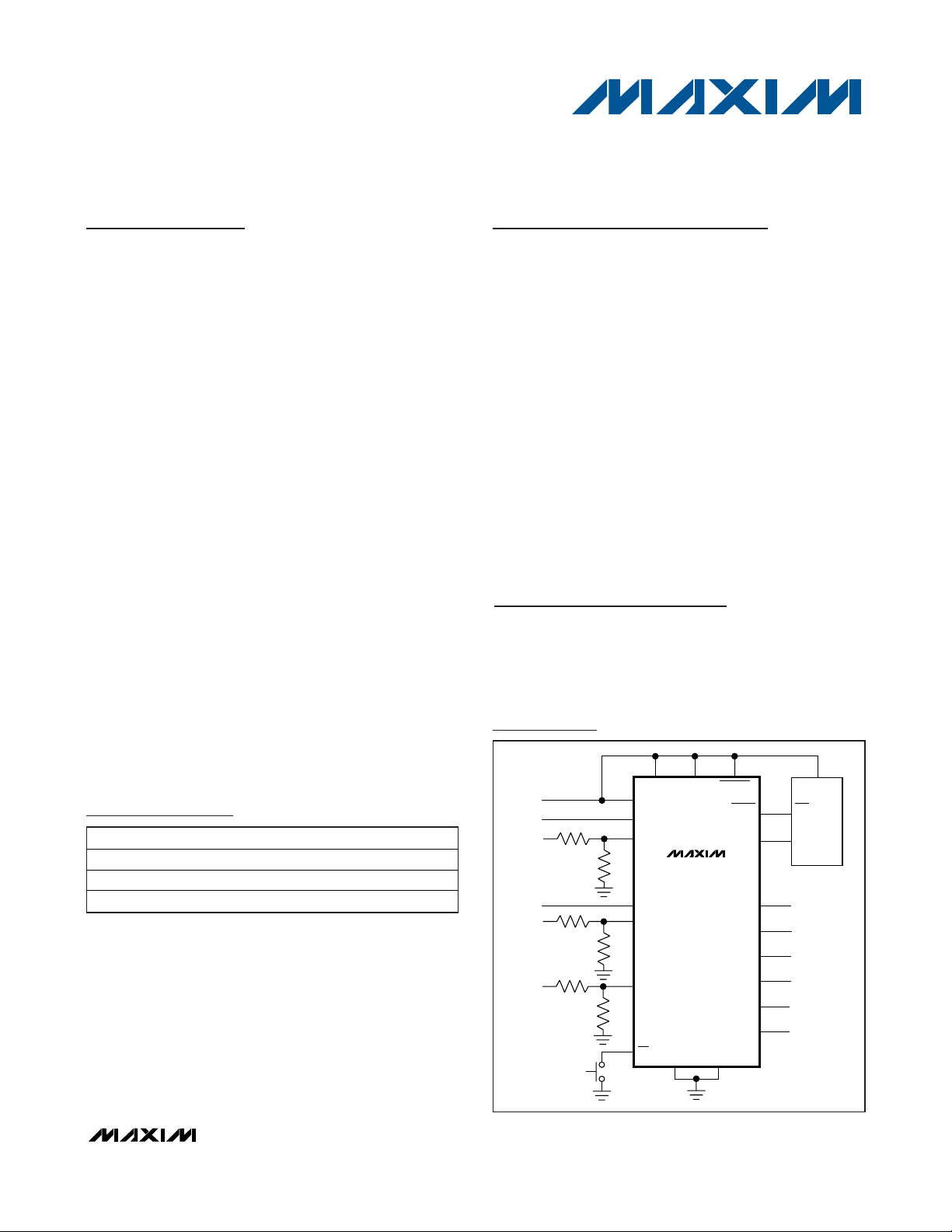
Ordering Information
Typical Operating Circuit
19-4099; Rev 0; 4/08
For pricing, delivery, and ordering information, please contact Maxim Direct at 1-888-629-4642,
or visit Maxim’s website at www.maxim-ic.com.
Note: The “_” is a placeholder for the input voltage threshold.
See Table 1. The MAX16060/MAX16061/MAX16062 are available in factory-preset thresholds/configuration combinations.
Choose the desired combination and complete part number
from Table 1.
+
Denotes a lead-free package.
For tape-and-reel, add a “T” after the “+.” Tape-and-reel are
offered in 2.5k increments.
*
EP = Exposed pad.
Storage Equipment
Servers
Networking/Telecommunication Equipment
Multivoltage ASICs
Automotive
Applications
V
SRT
MAX16061A
MARGIN
RESET
OUT1
OUT2
OUT3
OUT4
OUT5
OUT6
WDI
RST
I/O
PART TEMP RANGE PIN-PACKAGE
MAX16060_TE+ -40°C to +125°C 16 TQFN-EP*
MAX16061_TP+ -40°C to +125°C 20 TQFN-EP*
MAX16062_TG+ -40°C to +125°C 24 TQFN-EP*
CC
V
IN1
V
IN2
V
IN3
V
IN4
V
IN5
V
IN6
IN1
IN2
IN3
IN4
IN5
IN6
MR
GNDμPTOL
Page 2
MAX16060/MAX16061/MAX16062
1% Accurate, Quad-/Hex-/Octal-Voltage
µP Supervisors
2
______________________________________________________________________________________________________________________________________________________________________________
ABSOLUTE MAXIMUM RATINGS
ELECTRICAL CHARACTERISTICS
(VCC= 2.0V to 5.5V, TA= -40°C to +125°C, unless otherwise specified. Typical values are at VCC= 3.3V, TA= +25°C.) (Note 1)
Stresses beyond those listed under “Absolute Maximum Ratings” may cause permanent damage to the device. These are stress ratings only, and functional
operation of the device at these or any other conditions beyond those indicated in the operational sections of the specifications is not implied. Exposure to
absolute maximum rating conditions for extended periods may affect device reliability.
VCC, OUT_, IN_, RESET to GND ..............................-0.3V to +6V
TOL, MARGIN, MR, SRT, WDI to GND ...........-0.3V to V
CC
+ 0.3
Input/Output Current (RESET, MARGIN,
SRT, MR, TOL, OUT_, WDI).........................................±20mA
Continuous Power Dissipation (T
A
= +70°C)
16-Pin TQFN (derate 16.9mW/°C above +70°C) ......1349mW
20-Pin TQFN (derate 16.9mW/°C above +70°C) ......1355mW
24-Pin TQFN (derate 16.9mW/°C above +70°C) ......1666mW
Operating Temperature Range .........................-40°C to +125°C
Junction Temperature .....................................................+150°C
Storage Temperature Range .............................-65°C to +150°C
Lead Temperature (soldering, 10s) .................................+300°C
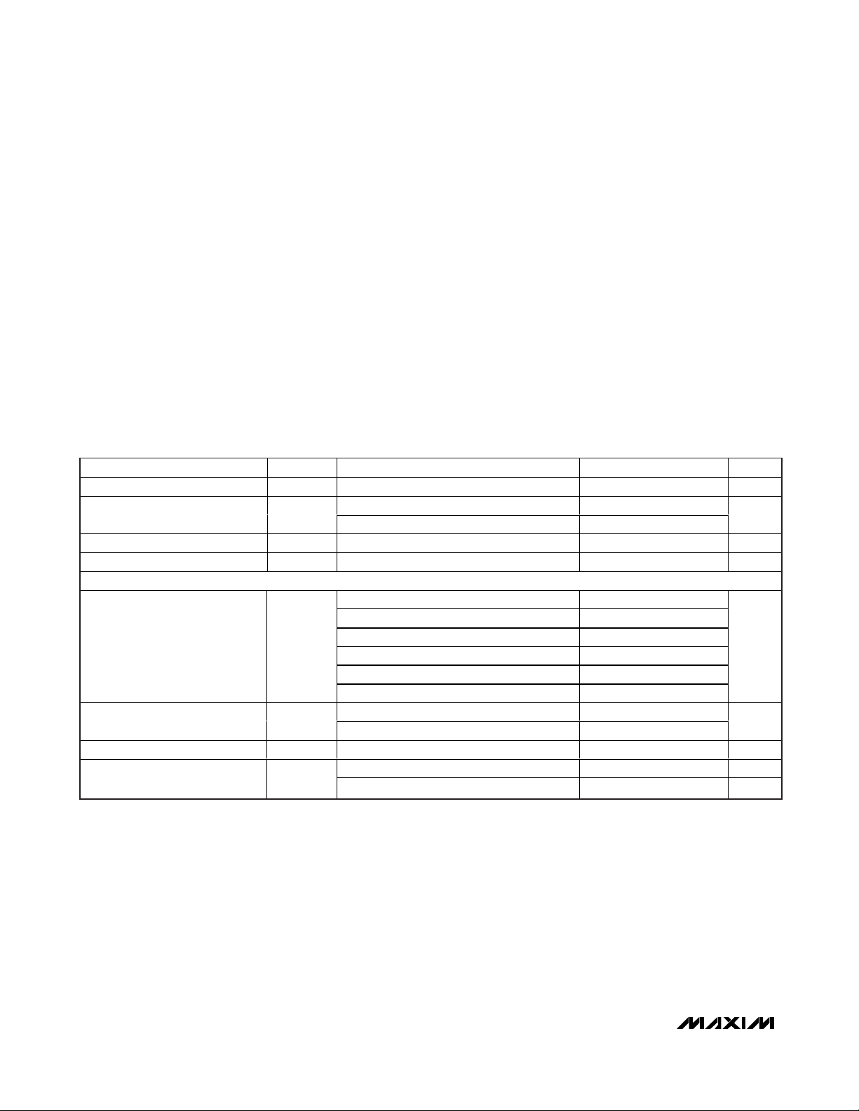
Operating Voltage Range V
Supply Current (Note 3) I
UVLO (Undervoltage Lockout) V
UVLO Hysteresis V
IN_ (See Table 1)
Threshold Voltages (IN_ Falling) V
Adjustable Threshold
(IN_ Falling)
IN_ Hysteresis VTH_
IN_ Input Current
PARAMETER SYMBOL CONDITIONS MIN TYP MAX UNITS
CC
CC
UVLO
UVLO_HYS
TH
V
TH
(Note 2) 1.0 5.5 V
VCC = 3.3V, OUT_, RESET not asserted 45 65
VCC = 5V, OUT_, RESET not asserted 50 70
V
rising 1.62 1.80 1.98 V
CC
3.3V threshold, TOL = GND 3.069 3.102 3.135
3.3V threshold, TOL = V
2.5V threshold, TOL = GND 2.325 2.350 2.375
2.5V threshold, TOL = V
1.8V threshold, TOL = GND 1.674 1.692 1.710
1.8V threshold, TOL = V
TOL = GND 0.390 0.394 0.398
TOL = V
IN_ rising 0.5 % V
HYS
Fixed thresholds 3 16 µA
Adjustable thresholds -100 +100 nA
CC
65 mV
CC
CC
CC
2.904 2.937 2.970
2.200 2.225 2.250
1.584 1.602 1.620
0.369 0.373 0.377
µA
V
V
TH
Page 3
MAX16060/MAX16061/MAX16062
1% Accurate, Quad-/Hex-/Octal-Voltage
µP Supervisors
______________________________________________________________________________________________________________________________________________________________________________
3
ELECTRICAL CHARACTERISTICS (continued)
(VCC= 2.0V to 5.5V, TA= -40°C to +125°C, unless otherwise specified. Typical values are at VCC= 3.3V, TA= +25°C.) (Note 1)
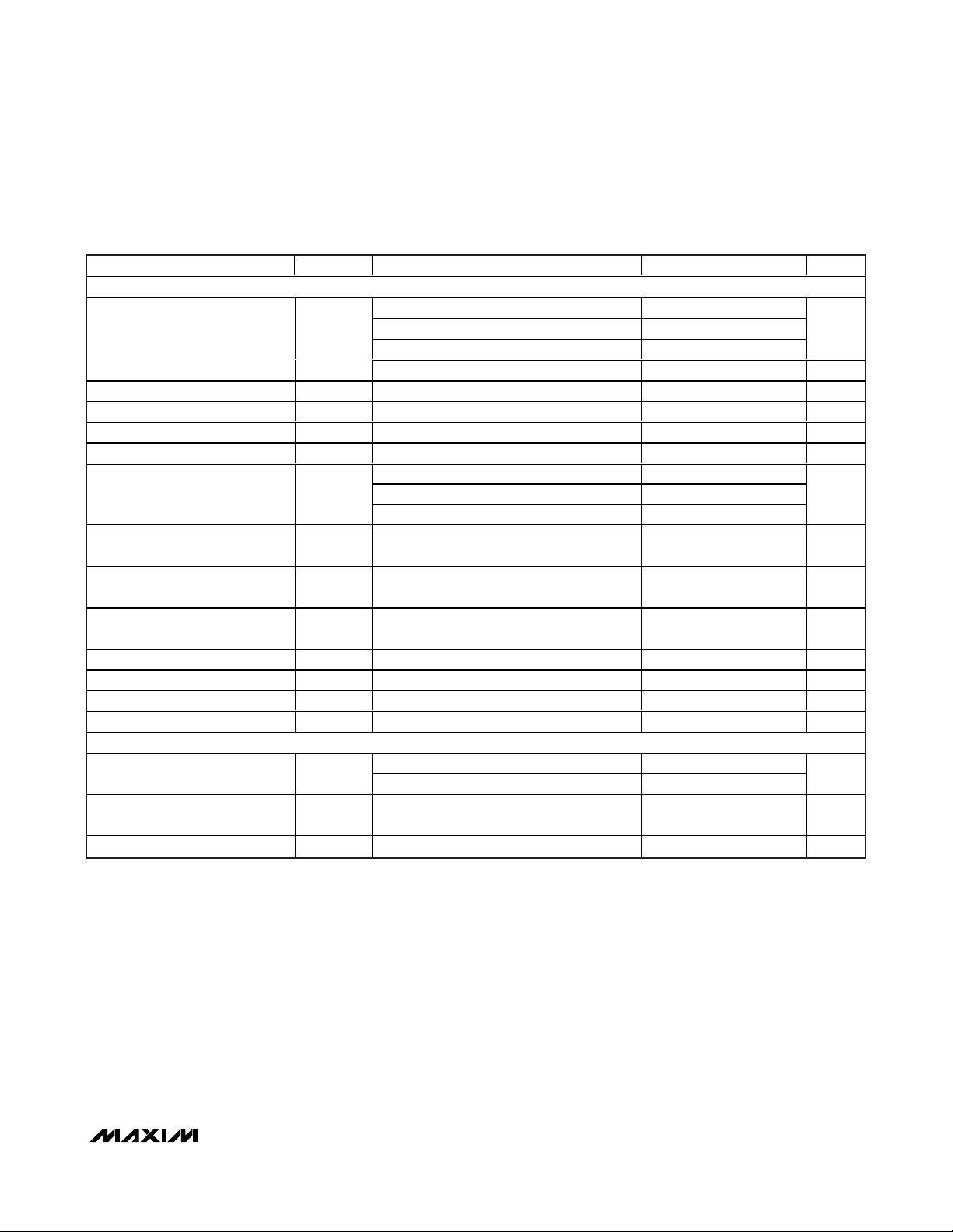
RESET
Reset Timeout t
SRT Ramp Current I
SRT Threshold 1.173 1.235 1.293 V
SRT Hysteresis 100 mV
IN_ to Reset Delay t
RESET Output-Voltage High V
MR Input-Voltage Low V
MR Input-Voltage High V
MR Minimum Pulse Width 1µs
MR Glitch Rejection 100 ns
MR to Reset Delay 200 ns
MR Pullup Resistance Pulled up to V
OUTPUTS (OUT_ )
OUT_ Output-Voltage Low V
OUT_ Output-Voltage High V
IN_ to OUT_ Propagation Delay t
PARAMETER SYMBOL CONDITIONS MIN TYP MAX UNITS
RP
SRT
RD
OL
OH
OL
OH
D
SRT = V
C
C
C
V
IN_ falling 20 µs
V
VCC = 2.5V, I
VCC = 1.2V, I
V
deasserted
IL
IH
VCC = 3.3V, I
VCC = 2.5V, I
V
(VTH + 100mV) to (VTH - 100mV) 20 µs
CC
= 1500pF (Note 4) 2.43 3.09 3.92
SRT
= 100pF 0.206
SRT
= open 50 µs
SRT
= 0V 460 600 740 nA
SRT
= 3.3V , I
C C
≥ 2.0V, I
CC
≥ 2.0V, I
CC
= 10m A, RESET asser ted 0.3
S IN K
= 6mA, RESET asser ted 0.3RESET Output-Voltage Low V
SINK
= 50µA, RESET asser ted 0.3
SINK
= 6µA, RESET
SOURCE
CC
= 2mA 0.3
SINK
= 1.2mA 0.3
SINK
= 6µA
SOURCE
140 200 280
0.8 x
V
CC
0.3 x
V
CC
0.7 x
V
CC
12 20 28 kΩ
0.8 x
V
CC
ms
V
V
V
V
V
V
Page 4
MAX16060/MAX16061/MAX16062
1% Accurate, Quad-/Hex-/Octal-Voltage
µP Supervisors
4
______________________________________________________________________________________________________________________________________________________________________________
ELECTRICAL CHARACTERISTICS (continued)
(VCC= 2.0V to 5.5V, TA= -40°C to +125°C, unless otherwise specified. Typical values are at VCC= 3.3V, TA= +25°C). (Note 1)
Note 1: Devices are tested at T
A
= +25°C and guaranteed by design for TA= T
MIN
to T
MAX
.
Note 2: The outputs are guaranteed to remain asserted down to V
CC
= 1V.
Note 3: Measured with WDI, MARGIN, and MR unconnected.
Note 4: The minimum and maximum specifications for this parameter are guaranteed by using the worst case of the SRT ramp cur-
rent and SRT threshold specifications.
Note 5: Guaranteed by design and not production tested.
Note 6: Amount of time required for logic to lock/unlock outputs from margin testing.
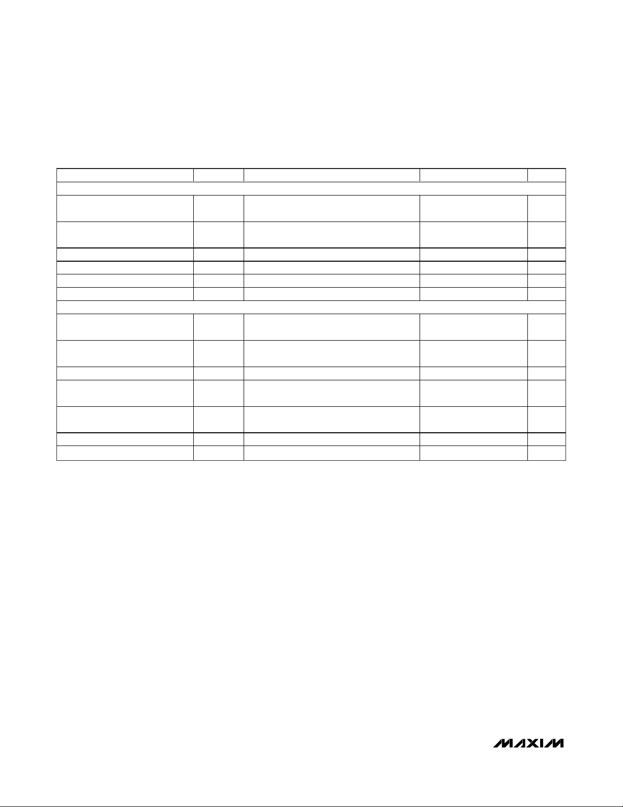
WATCHDOG TIMER
WDI Input-Voltage Low V
WDI Input-Voltage High V
WDI Pulse Width (Note 5) 50 ns
Watchdog Timeout Period t
Watchdog Startup Period 35 54 72 s
Watchdog Input Current V
DIGITAL LOGIC
TOL Input-Voltage Low V
TOL Input-Voltage High V
TOL Input Current TOL = V
MARGIN Input-Voltage Low V
MARGIN Input-Voltage High V
MARGIN Pullup Resistance Pulled up to V
MARGIN Delay Time t
PARAMETER SYMBOL CONDITIONS MIN TYP MAX UNITS
IL
IH
WDI
IL
IH
IL
IH
MD
0.7 x
V
CC
1.12 1.60 2.40 s
= 0 to VCC (Note 5) -1 +1 µA
WDI
0.7 x
V
CC
CC
0.7 x
V
CC
CC
Rising or falling (Note 6) 50 µs
12 20 28 kΩ
0.3 x
V
CC
0.3 x
V
CC
100 nA
0.3 x
V
CC
V
V
V
V
V
V
Page 5
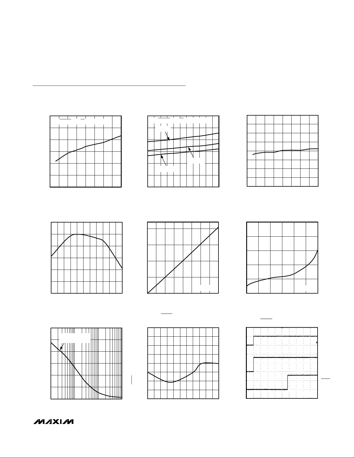
Typical Operating Characteristics
(VCC= 3.3V, TA = +25°C, unless otherwise noted.)
SUPPLY CURRENT vs. SUPPLY VOLTAGE
SUPPLY VOLTAGE (V)
SUPPLY CURRENT (μA)
MAX16060/1/2 toc01
1.5 2.0 2.5 3.0 3.5 4.0 4.5 5.0 5.5
30
35
40
45
50
55
60
WDI, MARGIN, AND MR UNCONNECTED
SUPPLY CURRENT vs. TEMPERATURE
TEMPERATURE (°C)
SUPPLY CURRENT (μA)
MAX16060/1/2 toc02
-40 -25 -10 5 20 35 50 65 80 95 110 125
30
35
40
45
50
55
60
WDI, MARGIN, AND MR UNCONNECTED
VCC = 2.5V
VCC = 3.3V
VCC = 5V
NORMALIZED THRESHOLD
vs. SUPPLY VOLTAGE
SUPPLY VOLTAGE (V)
NORMALIZED THRESHOLD
MAX16060/1/2 toc03
1.5 2.0 2.5 3.0 3.5 4.0 4.5 5.0 5.5
0.9900
0.9925
0.9950
0.9975
1.0000
1.0025
1.0050
1.0075
1.0100
NORMALIZED THRESHOLD
vs. TEMPERATURE
TEMPERATURE (°C)
NORMALIZED THRESHOLD
MAX16060/1/2 toc04
-40 -25 -10 5 20 35 50 65 80 95 110 125
0.995
0.996
0.997
0.998
0.999
1.000
1.001
OUTPUT VOLTAGE vs. SINK CURRENT
SINK CURRENT (mA)
V
OUT
_ (mV)
MAX16060/1/2 toc05
012345678
0
25
50
75
100
OUT_ LOW
OUTPUT VOLTAGE vs. SOURCE CURRENT
SOURCE CURRENT (μA)
V
CC
- V
OUT_
(mV)
MAX16060/1/2 toc06
0 5 10 15 20 25 30
0
200
400
600
800
1000
OUT_ HIGH
RESET TIMEOUT PERIOD
vs. TEMPERATURE
TEMPERATURE (°C)
RESET TIMEOUT PERIOD (ms)
MAX16060/1/2 toc08
-40 -25 -10 5 20 35 50 65 80 95 110 125
190
191
192
193
194
195
196
197
198
1 10 100 1000
MAXIMUM TRANSIENT DURATION
vs. INPUT OVERDRIVE
MAX16060/1/2 toc07
INPUT OVERDRIVE (mV)
MAXIMUM TRANSIENT DURATION (μs)
600
0
100
200
300
400
500
OUTPUT GOES LOW
ABOVE THIS LINE
RESET TIMEOUT DELAY
MAX16060/1/2 toc09
OUT1
2V/div
IN1
5V/div
40ms/div
RESET
2V/div
SRT = V
CC
MAX16060/MAX16061/MAX16062
1% Accurate, Quad-/Hex-/Octal-Voltage
µP Supervisors
_______________________________________________________________________________________
5
Page 6
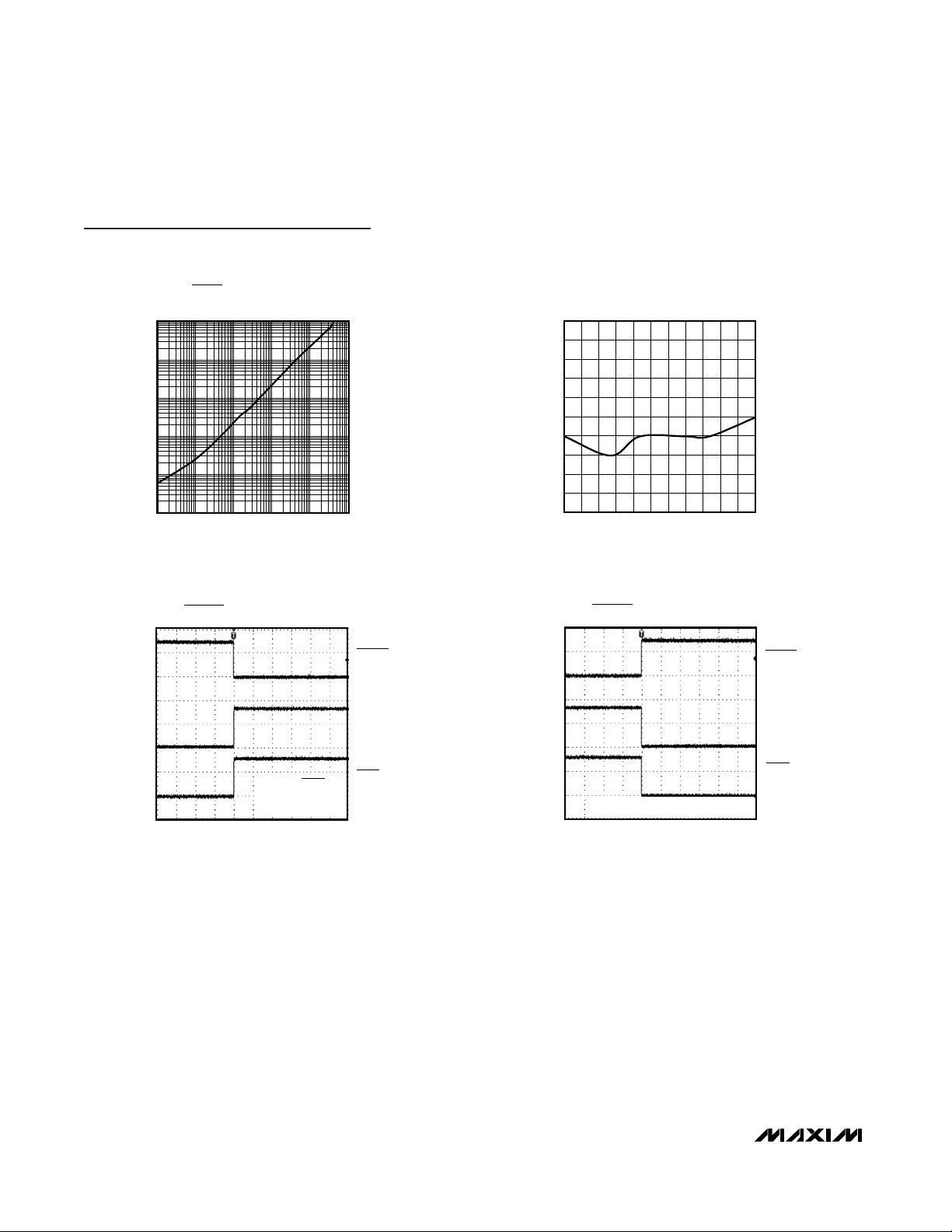
Typical Operating Characteristics (continued)
(VCC= 3.3V, TA = +25°C, unless otherwise noted.)
MARGIN DISABLE FUNCTION
MAX16060/1/2 toc13
OUT_
2V/div
MARGIN
2V/div
100μs/div
RESET
2V/div
OUT_ AND RESET ARE BELOW RESPECTIVE
THRESHOLDS
WATCHDOG TIMEOUT PERIOD
vs. TEMPERATURE
TEMPERATURE (°C)
WATCHDOG TIMEOUT PERIOD (s)
MAX16060/1/2 toc11
-40 -25 -10 5 20 35 50 65 80 95 110 125
1.50
1.51
1.52
1.53
1.54
1.55
1.56
1.57
1.58
1.59
1.60
MARGIN ENABLE FUNCTION
MAX16060/1/2 toc12
OUT_
2V/div
MARGIN
2V/div
100μs/div
RESET
2V/div
OUT_ AND RESET ARE
BELOW RESPECTIVE
THRESHOLDS
1000
0.01 0.1 1 10 100 1000
100
10
1
0.1
0.01
RESET TIMEOUT PERIOD
vs. C
SRT
MAX16060/1/2 toc10
C
SRT
(nF)
t
RP
(ms)
MAX16060/MAX16061/MAX16062
1% Accurate, Quad-/Hex-/Octal-Voltage
µP Supervisors
6
______________________________________________________________________________________________________________________________________________________________________________
Page 7

MAX16060/MAX16061/MAX16062
1% Accurate, Quad-/Hex-/Octal-Voltage
µP Supervisors
______________________________________________________________________________________________________________________________________________________________________________
7
Pin Description (MAX16060)
PIN NAME FUNCTION
1 IN3 Monitored Input Voltage 3. See Table 1 for the input voltage threshold.
2 IN4 Monitored Input Voltage 4. See Table 1 for the input voltage threshold.
Watchdog Timer Input. If WDI remains low or high for longer than the watchdog timeout period, RESET
is asserted. The timer clears whenever a reset is asserted or a rising or falling edge on WDI is detected.
3 WDI
4 GND Ground
5VCCUnmonitored Power-Supply Input
6 OUT3
7 OUT4
8 MR
9 SRT
10 MARGIN
11 OUT2
12 OUT1
13 RESET
14 IN1 Monitored Input Voltage 1. See Table 1 for the input voltage threshold.
15 IN2 Monitored Input Voltage 2. See Table 1 for the input voltage threshold.
16 TOL
—EP
The watchdog timer enters a startup period that allows 54s for the first transition to occur before a reset.
Leave WDI unconnected to disable the watchdog timer. The WDI unconnected-state detector uses a
small 400nA current. Therefore, do not connect WDI to anything that will source or sink more than
200nA. Note that the leakage current specification for most three-state drivers exceeds 200nA.
O utp ut 3. When the vol tag e at IN 3 fal l s b el ow i ts thr eshol d , OU T3 g oes l ow and stays l ow unti l the vol tag e at
IN 3 exceed s i ts thr eshol d . The op en- d r ai n outp ut has a 30µA i nter nal p ul l up to V
O utp ut 4. When the vol tag e at IN 4 fal l s b el ow i ts thr eshol d , OU T4 g oes l ow and stays l ow unti l the vol tag e at
IN 4 exceed s i ts thr eshol d . The op en- d r ai n outp ut has a 30µA i nter nal p ul l up to V
Active-Low Manual Reset Input. Pull MR low to assert RESET low. RESET remains low for the reset
timeout period after MR is deasserted. MR is pulled up to V
Set Reset Timeout Input. Connect a capacitor from SRT to GND to set the reset timeout period. The reset
timeout period can be calculated as follows:
Reset Timeout (s) = 2.06 x 10
SRT to V
Active-Low Manual Deassert Input. Pull MARGIN low to deassert all outputs (go into high state),
regardless of the voltage at any monitored input.
O utp ut 2. When the vol tag e at IN 2 fal l s b el ow i ts thr eshol d , OU T2 g oes l ow and stays l ow unti l the vol tag e at
IN 2 exceed s i ts thr eshol d . The op en- d r ai n outp ut has a 30µA i nter nal p ul l up to V
O utp ut 1. When the vol tag e at IN 1 fal l s b el ow i ts thr eshol d , OU T1 g oes l ow and stays l ow unti l the vol tag e at
IN 1 exceed s i ts thr eshol d . The op en- d r ai n outp ut has a 30µA i nter nal p ul l up to V
Active-Low Reset Output. RESET asserts low when any of the monitored voltages falls below its
respective threshold or MR is asserted. RESET remains asserted for the reset timeout period after all
monitored voltages exceed their respective thresholds and MR is deasserted. This open-drain output
has a 30µA internal pullup.
Threshold Tolerance Input. Connect TOL to GND to select 5% threshold tolerance. Connect TOL to V
to select 10% threshold tolerance.
Exposed Pad. EP is internally connected to GND. Connect EP to the ground plane to provide a low
thermal resistance path from the IC junction to the PCB. Do not use as the electrical connection to GND.
CC
.
6
(Ω) x C
(F). For the internal timeout period of 140ms (min), connect
SRT
through a 20kΩ resistor.
CC
C C
C C
C C
C C
.
.
.
.
CC
Page 8

MAX16060/MAX16061/MAX16062
1% Accurate, Quad-/Hex-/Octal-Voltage
µP Supervisors
8
______________________________________________________________________________________________________________________________________________________________________________
Pin Description (MAX16061)
PIN NAME FUNCTION
1 IN4 Monitored Input Voltage 4. See Table 1 for the input voltage threshold.
2 IN5 Monitored Input Voltage 5. See Table 1 for the input voltage threshold.
3 IN6 Monitored Input Voltage 6. See Table 1 for the input voltage threshold.
Watchdog Timer Input. If WDI remains low or high for longer than the watchdog timeout period, RESET is
asserted and the timer is cleared. The timer also clears whenever a reset is asserted or a rising or falling
edge on WDI is detected. The watchdog timer enters a startup period that allows 54s for the first transition to
4 WDI
5 GND Ground
6VCCUnmonitored Power-Supply Input
7 OUT4
8 OUT5
9 OUT6
10 MR
11 SRT
12 MARGIN
13 OUT3
14 OUT2
15 OUT1
16 RESET
17 IN1 Monitored Input Voltage 1. See Table 1 for the input voltage threshold.
18 IN2 Monitored Input Voltage 2. See Table 1 for the input voltage threshold.
19 IN3 Monitored Input Voltage 3. See Table 1 for the input voltage threshold.
20 TOL
—EP
occur before a reset. Leave WDI unconnected to disable the watchdog timer.
The WDI unconnected-state detector uses a small 400nA current. Therefore, do not connect WDI to anything
that will source or sink more than 200nA. Note that the leakage current specification for most three-state
drivers exceeds 200nA.
Output 4. When the voltage at IN4 falls below its threshold, OUT4 goes low and stays low until the voltage at
IN4 exceeds its threshold. The open-drain output has a 30µA internal pullup to V
Output 5. When the voltage at IN5 falls below its threshold, OUT5 goes low and stays low until the voltage at
IN5 exceeds its threshold. The open-drain output has a 30µA internal pullup to V
Output 6. When the voltage at IN6 falls below its threshold, OUT6 goes low and stays low until the voltage at
IN6 exceeds its threshold. The open-drain output has a 30µA internal pullup to V
Active-Low Manual Reset Input. Pull MR low to assert RESET low. RESET remains low for the reset timeout
period after MR is deasserted. MR is pulled up to V
Set Reset Timeout Input. Connect a capacitor from SRT to GND to set the reset timeout period. The reset
timeout period can be calculated as follows:
Reset Timeout (s) = 2.06 x 10
.
V
CC
Manual Deassert Input. Pull MARGIN low to deassert all outputs (go into high state), regardless of the voltage
at any monitored input.
Output 3. When the voltage at IN3 falls below its threshold, OUT3 goes low and stays low until the voltage at
IN3 exceeds its threshold. The open-drain output has a 30µA internal pullup to V
Output 2. When the voltage at IN2 falls below its threshold, OUT2 goes low and stays low until the voltage at
IN2 exceeds its threshold. The open-drain output has a 30µA internal pullup to V
Output 1. When the voltage at IN1 falls below its threshold, OUT1 goes low and stays low until the voltage at
IN1 exceeds its threshold. The open-drain output has a 30µA internal pullup to V
Active-Low Reset Output. RESET asserts low when any of the monitored voltages falls below its respective
threshold or MR is asserted. RESET remains asserted for the reset timeout period after all monitored voltages
exceed their respective thresholds and MR is deasserted. This open-drain output has a 30µA internal pullup.
Threshold Tolerance Input. Connect TOL to GND to select 5% threshold tolerance. Connect TOL to V
select 10% threshold tolerance.
Exposed Pad. EP is internally connected to GND. Connect EP to the ground plane to provide a low thermal
resistance path from the IC junction to the PCB. Do not use as the electrical connection to GND.
6
(Ω) x C
(F). For the internal timeout period of 140ms (min), connect SRT to
SRT
through a 20kΩ resistor.
CC
CC
CC
CC
CC
CC
CC
.
.
.
.
.
.
to
CC
Page 9

MAX16060/MAX16061/MAX16062
1% Accurate, Quad-/Hex-/Octal-Voltage
µP Supervisors
______________________________________________________________________________________________________________________________________________________________________________
9
Pin Description (MAX16062)
PIN NAME FUNCTION
1 IN5 Monitored Input Voltage 5. See Table 1 for the input voltage threshold.
2 IN6 Monitored Input Voltage 6. See Table 1 for the input voltage threshold.
3 IN7 Monitored Input Voltage 7. See Table 1 for the input voltage threshold.
4 IN8 Monitored Input Voltage 8. See Table 1 for the input voltage threshold.
Watchdog Timer Input. If WDI remains low or high for longer than the watchdog timeout period, RESET is
asserted and the timer is cleared. The timer also clears whenever a reset is asserted or a rising or falling edge on
5 WDI
6 GND Ground
7VCCUnmonitored Power-Supply Input
8 OUT5
9 OUT6
10 OUT7
11 OUT8
12 MR
13 SRT
14 MARGIN
15 OUT4
16 OUT3
17 OUT2
18 OUT1
19 RESET
20 IN1 Monitored Input Voltage 1. See Table 1 for the input voltage threshold.
21 IN2 Monitored Input Voltage 2. See Table 1 for the input voltage threshold.
22 IN3 Monitored Input Voltage 3. See Table 1 for the input voltage threshold.
23 IN4 Monitored Input Voltage 4. See Table 1 for the input voltage threshold.
24 TOL
—EP
WDI is detected. The watchdog timer enters a startup period that allows 54s for the first transition to occur before
a reset. Leave WDI unconnected to disable the watchdog timer. The WDI unconnected state detector uses a
small 400nA current. Therefore, do not connect WDI to anything that will source or sink more than 200nA. Note
that the leakage current specification for most three-state drivers exceeds 200nA.
Output 5. When the voltage at IN5 falls below its threshold, OUT5 goes low and stays low until the voltage at IN5
exceeds its threshold. The open-drain output has a 30µA internal pullup to V
Output 6. When the voltage at IN6 falls below its threshold, OUT6 goes low and stays low until the voltage at IN6
exceeds its threshold. The open-drain output has a 30µA internal pullup to V
Output 7. When the voltage at IN7 falls below its threshold, OUT7 goes low and stays low until the voltage at IN7
exceeds its threshold. The open-drain output has a 30µA internal pullup to V
Output 8. When the voltage at IN8 falls below its threshold, OUT8 goes low and stays low until the voltage at IN8
exceeds its threshold. The open-drain output has a 30µA internal pullup to V
Active-Low Manual Reset Input. Pull MR low to assert RESET low. RESET remains low for the reset timeout period
after MR is deasserted. MR is pulled up to V
Set Reset Timeout Input. Connect a capacitor from SRT to GND to set the reset timeout period. The reset timeout
period can be calculated as follows:
Reset Ti m eout ( s) = 2.06 x 10
Margin Disable Input. Pull MARGIN low to deassert all outputs (go into high state), regardless of the voltage at
any monitored input.
Output 4. When the voltage at IN4 falls below its threshold, OUT4 goes low and stays low until the voltage at IN4
exceeds its threshold. The open-drain output has a 30µA internal pullup to V
Output 3. When the voltage at IN3 falls below its threshold, OUT3 goes low and stays low until the voltage at IN3
exceeds its threshold. The open-drain output has a 30µA internal pullup to V
Output 2. When the voltage at IN2 falls below its threshold, OUT2 goes low and stays low until the voltage at IN2
exceeds its threshold. The open-drain output has a 30µA internal pullup to V
Output 1. When the voltage at IN1 falls below its threshold, OUT1 goes low and stays low until the voltage at IN1
exceeds its threshold. The open-drain output has a 30µA internal pullup to V
Active-Low Reset Output. RESET asserts low when any of the monitored voltages falls below its respective
threshold or MR is asserted. RESET remains asserted for the reset timeout period after all monitored voltages
exceed their respective thresholds and MR is deasserted. This open-drain output has a 30µA internal pullup.
Threshold Tolerance Input. Connect TOL to GND to select 5% threshold tolerance. Connect TOL to V
10% threshold tolerance.
E xp osed P ad . E P i s i nter nal l y connected to GN D . C onnect E P to the g r ound p l ane to p r ovi d e a l ow ther m al r esi stance
p ath fr om the IC j uncti on to the P C B. D o not use as the el ectr i cal connecti on to GN D .
6
( Ω) x C
S RT
through a 20kΩ resistor.
CC
( F) . For the i nter nal ti m eout p er i od of 140m s ( m i n) , connect S RT to V
CC
CC
CC
CC
CC
CC
CC
CC
.
.
.
.
.
C C
.
.
.
.
to select
CC
Page 10
MAX16060/MAX16061/MAX16062
1% Accurate, Quad-/Hex-/Octal-Voltage
µP Supervisors
10
____________________________________________________________________________________________________________________________________________________________________________
Table 1. Input-Voltage-Threshold Selector
Note: Other fixed thresholds may be available. Contact factory for availability.
PART IN1 IN2 IN3 IN4 IN5 IN6 IN7 IN8
MAX16060A 3.3 2.5 ADJ 1.8 — — — —
MAX16060B 3.3 ADJ ADJ 1.8 — — — —
MAX16060C ADJ 2.5 ADJ 1.8 — — — —
MAX16060D 3.3 2.5 ADJ ADJ — — — —
MAX16060E ADJ ADJ ADJ ADJ — — — —
MAX16061A 3.3 2.5 ADJ 1.8 ADJ ADJ — —
MAX16061B 3.3 ADJ ADJ 1.8 ADJ ADJ — —
MAX16061C 3.3 2.5 ADJ ADJ ADJ ADJ — —
MAX16061D ADJ 2.5 ADJ 1.8 ADJ ADJ — —
MAX16061E ADJ ADJ ADJ ADJ ADJ ADJ — —
MAX16062A 3.3 2.5 ADJ 1.8 ADJ ADJ ADJ ADJ
MAX16062B 3.3 ADJ ADJ 1.8 ADJ ADJ ADJ ADJ
MAX16062C 3.3 2.5 ADJ ADJ ADJ ADJ ADJ ADJ
MAX16062D ADJ 2.5 ADJ 1.8 ADJ ADJ ADJ ADJ
MAX16062E ADJ ADJ ADJ ADJ ADJ ADJ ADJ ADJ
Page 11

MAX16060/MAX16061/MAX16062
IN1
Figure 1. MAX16060D Functional Diagram
Functional Diagrams
1% Accurate, Quad-/Hex-/Octal-Voltage
µP Supervisors
____________________________________________________________________________________________________________________________________________________________________________
11
IN2
IN3
MR SRTWDI
V
CC
V
CC
WATCHDOG
TIMER CIRCUIT
TIMING
RESET CIRCUIT
RESET
OUT1
OUT2
OUTPUT
DRIVER
OUT3
IN4
TOL
V
CC
REFERENCE
V
UNDERVOLTAGE LOCKOUT
EN
CC
V
CC
MARGIN
MAX16060D
OUT4
Page 12

MAX16060/MAX16061/MAX16062
1% Accurate, Quad-/Hex-/Octal-Voltage
µP Supervisors
12
____________________________________________________________________________________________________________________________________________________________________________
Figure 2. MAX16061C Functional Diagram
Functional Diagrams (continued)
MR SRTWDI
V
CC
V
CC
IN1
IN2
IN3
WATCHDOG
TIMER CIRCUIT
TIMING
RESET CIRCUIT
RESET
OUT1
OUT2
OUTPUT
DRIVER
IN4
IN5
IN6
TOL
V
CC
REFERENCE
V
CC
UNDERVOLTAGE LOCKOUT
V
CC
EN
MARGIN
OUT3
OUT4
OUT5
OUT6
MAX16061C
Page 13

MAX16060/MAX16061/MAX16062
Figure 3. MAX16062C Functional Diagram
Functional Diagrams (continued)
1% Accurate, Quad-/Hex-/Octal-Voltage
µP Supervisors
____________________________________________________________________________________________________________________________________________________________________________
13
MR SRTWDI
V
V
WATCHDOG
TIMER CIRCUIT
IN1
IN2
IN3
CC
TIMING
RESET CIRCUIT
CC
RESET
OUT1
OUT2
TOL
OUTPUT
DRIVER
IN4
IN5
IN6
IN7
IN8
V
CC
REFERENCE
V
CC
UNDERVOLTAGE LOCKOUT
V
CC
EN
MAX16062C
OUT3
OUT4
OUT5
OUT6
OUT7
OUT8
MARGIN
Page 14

MAX16060/MAX16061/MAX16062
1% Accurate, Quad-/Hex-/Octal-Voltage
µP Supervisors
14
____________________________________________________________________________________________________________________________________________________________________________
Detailed Description
The MAX16060/MAX16061/MAX16062 are 1% accurate
low-voltage, quad-/hex-/octal-voltage µP supervisors in
a small thin QFN package. These devices provide
supervisory functions for complex multivoltage systems.
The MAX16060 monitors four voltages; the MAX16061
monitors six voltages; and the MAX16062 monitors eight
voltages.
These supervisors offer independent outputs for each
monitored voltage along with a reset output that asserts
whenever any of the monitored voltages fall below their
respective thresholds or the manual reset input is
asserted. The reset output remains asserted for the
reset timeout after all voltages are above their respective thresholds and the manual reset input is deasserted. The minimum reset timeout is internally set to
140ms or can be adjusted with an external capacitor.
All open-drain outputs have internal 30µA pullups that
eliminate the need for external pullup resistors.
However, each output can be driven with an external
voltage up to 5.5V. Other features offered include a
manual reset input, a tolerance pin for selecting 5% or
10% input thresholds, and a margin enable function for
deasserting the outputs during margin testing.
An additional feature is a watchdog timer that asserts
RESET when the watchdog timeout period (1.6s typ) is
exceeded. The watchdog timer can be disabled by
leaving WDI unconnected.
Applications Information
Undervoltage-Detection Circuit
The open-drain outputs of the MAX16060/
MAX16061/MAX16062 can be configured to detect an
undervoltage condition. Figure 4 shows a configuration
where an LED turns on when the comparator output is
low, indicating an undervoltage condition. These
devices can also be used in applications such as system supervisory monitoring, multivoltage level detection,
and VCCbar-graph monitoring (Figure 5).
Tolerance (TOL)
The MAX16060/MAX16061/MAX16062 feature a pinselectable threshold tolerance. Connect TOL to GND to
select 5% threshold tolerance. Connect TOL to VCCto
select 10% threshold tolerance.
Window Detection
A window detector circuit uses two inputs in the configuration shown in Figure 6. External resistors set the two
threshold voltages of the window detector circuit.
External logic gates create the OUT signal. The window
detection width is the difference between the threshold
voltages (Figure 7).
Figure 4. Quad Undervoltage Detector with LED Indicators
Figure 5. VCCBar-Graph Monitoring
5V
V
IN1V1
V2
IN2
V3
IN3
V4
IN4
CC
MAX16060
GND
OUT1
OUT2
OUT3
OUT4
5V
D1
V
(5V)
IN
IN1
IN2
IN3
IN4
V
CC
MAX16060
GND
OUT1
OUT2
OUT3
OUT4
D2
D3
D4
Page 15

MAX16060/MAX16061/MAX16062
1% Accurate, Quad-/Hex-/Octal-Voltage
µP Supervisors
____________________________________________________________________________________________________________________________________________________________________________
15
Adjustable Input
These devices offer several monitor options with
adjustable input thresholds (see Table 1). The threshold
voltage at each adjustable IN_ input is typically 0.394V
(TOL = GND) or 0.373V (TOL = VCC). To monitor a voltage V
INTH
, connect a resistive-divider network to the cir-
cuit as shown in Figure 8.
V
INTH
= VTH((R1/R2) + 1)
R1 = R2 ((V
INTH/VTH
) - 1)
Large resistors can be used to minimize current through
the external resistors. For greater accuracy, use lowervalue resistors.
Unused Inputs
Connect any unused IN_ inputs to a voltage above its
threshold.
OUT_
Outputs
The OUT_ outputs go low when their respective IN_
inputs drop below their specified thresholds. The output
is open drain with a 30µA internal pullup to VCC. For
many applications, no external pullup resistor is required
to interface with other logic devices. An external pullup
resistor to any voltage from 0 to 5.5V overrides the internal pullup if interfacing to different logic supply voltages.
Internal circuitry prevents reverse current flow from the
external pullup voltage to V
CC
(Figure 9).
V
Figure 6. Window Detection
Figure 8. Setting the Adjustable Input
Figure 7. Output Response of Window Detector Circuit
INPUT
TH1 =
(1 + R1) (V
R2
R1
R2
+ V
TH
TH_HYS
IN1
IN2
)
5V
V
CC
MAX16060E
OUT1
OUT2
OUT
V
INTH
R1
R2
V
TH4 =
R3
R4
(1 + R3) V
R4
IN3
IN4
TH
OUT3
OUT4
GND
OUT1
OUT4
OUT
V
TH1
V
TH4
ΔV
TH
V
TH
R1 =
R2(
V
INTH
- 1
)
V
TH
Page 16

MAX16060/MAX16061/MAX16062
1% Accurate, Quad-/Hex-/Octal-Voltage
µP Supervisors
16
____________________________________________________________________________________________________________________________________________________________________________
RESET
Output
RESET asserts low when any of the monitored voltages
fall below their respective thresholds or MR is asserted.
RESET remains asserted for the reset timeout period
after all monitored voltages exceed their respective
thresholds and MR is deasserted (see Figure 10). This
open-drain output has a 30µA internal pullup. An external
pullup resistor to any voltage from 0 to 5.5V overrides the
internal pullup if interfacing to different logic supply voltages. Internal circuitry prevents reverse current flow from
the external pullup voltage to VCC(Figure 9).
Reset Timeout Capacitor
The reset timeout period can be adjusted to accommodate a variety of µP applications. Adjust the reset timeout period (tRP) by connecting a capacitor (C
SRT
)
between SRT and GND. Calculate the reset timeout
capacitor as follows:
Connect SRT to VCCfor a factory-programmed reset
timeout of 140ms (min).
Manual Reset Input (MR)
Many µP-based products require manual reset capability, allowing the operator, a test technician, or external
logic circuitry to initiate a reset. A logic-low on MR
asserts RESET low. RESET remains asserted while MR
is low, and during the reset timeout period (140ms min)
after MR returns high. The MR input has an internal
20kΩ pullup resistor to VCC, so it can be left unconnected if not used. MR can be driven with TTL or
CMOS-logic levels, or with open-drain/collector outputs.
Connect a normally open momentary switch from MR to
GND to create a manual reset function. External
debounce circuitry is not required. If MR is driven from
long cables or if the device is used in a noisy environment, connecting a 0.1µF capacitor from MR to GND
provides additional noise immunity.
CF
tsxI
V
SRT
RP
SRT
TH SRT
()
()
_
=
Figure 9. Interfacing to a Different Logic Supply Voltage
Figure 10. Output Timing Diagram
VCC = 3.3V
100kΩ
V
CC
OUT_
MAX16060
MAX16061
MAX16062
GND
RESET
5V
V
CC
GND
IN_
V
TH_
RESET
OUT_
V
TH_
90%
10%
t
RD
10%
t
D
t
RP
90%
t
D
Page 17

MAX16060/MAX16061/MAX16062
1% Accurate, Quad-/Hex-/Octal-Voltage
µP Supervisors
____________________________________________________________________________________________________________________________________________________________________________
17
Margin Output Disable (
MARGIN
)
MARGIN allows system-level testing while power supplies are adjusted from their nominal voltages. Drive
MARGIN low to force RESET and OUT_ high, regardless of the voltage at any monitored input. The state of
each output does not change while MARGIN = GND.
The watchdog timer continues to run when
MARGIN is low, and if a timeout occurs, RESET will
assert t
MD
after MARGIN is deasserted.
The MARGIN input is internally pulled up to VCC. Leave
MARGIN unconnected or connect to VCCif unused.
Undervoltage Lockout (UVLO)
The MAX16060/MAX16061/MAX16062 feature a V
CC
undervoltage lockout (UVLO) that preserves a reset
status even if V
CC
falls as low as 1V. The undervoltage
lockout circuitry monitors the voltage at VCC. If V
CC
falls below the UVLO falling threshold (typically
1.735V), RESET is asserted and all OUT_ are asserted
low. This eliminates an incorrect RESET or OUT_ output
state as V
CC
drops below the normal VCCoperational
voltage range of 1.98V to 5.5V.
During power-up as VCCrises above 1V, RESET is
asserted and all OUT_ are asserted low until V
CC
exceeds the UVLO threshold. As VCCexceeds the UVLO
threshold, all inputs are monitored and the correct output
state appears at all the outputs. This also ensures that
RESET and all OUT_ are in the correct state once V
CC
reaches the normal VCCoperational range.
Power-Supply Bypassing
In noisy applications, bypass VCCto ground with a
0.1µF capacitor as close to the device as possible. The
additional capacitor improves transient immunity. For
fast-rising VCCtransients, additional capacitance may
be required.
Page 18

MAX16060/MAX16061/MAX16062
1% Accurate, Quad-/Hex-/Octal-Voltage
µP Supervisors
Maxim cannot assume responsibility for use of any circuitry other than circuitry entirely embodied in a Maxim product. No circuit patent licenses are
implied. Maxim reserves the right to change the circuitry and specifications without notice at any time.
18
____________________Maxim Integrated Products, 120 San Gabriel Drive, Sunnyvale, CA 94086 408-737-7600
© 2008 Maxim Integrated Products is a registered trademark of Maxim Integrated Products, Inc.
Pin Configurations
Chip Information
PROCESS: BiCMOS
Package Information
For the latest package outline information, go to
www.maxim-ic.com/packages
.
PACKAGE TYPE PACKAGE CODE DOCUMENT NO.
16 TQFN T1644-4
21-0139
20 TQFN T2044-3
21-0139
24 TQFN T2444-4
21-0139
TOP VIEW
RESET
IN1
IN2
TOL
12 11 9
13
14
15
16
+
12
OUT2
OUT1
10
MAX16060
3
IN4
IN3
WDI MARGIN
THIN QFN
(4mm x 4mm)
SRT
4
GND
TOP VIEW
RESET
IN1
IN2
IN3
TOP VIEW
OUT2
OUT1
15 14 12 11
RESET
IN1
IN2
IN3
TOL
16
17
18
19
20
MAX16061
+
12
IN5
IN4
MR
8
7
OUT4
OUT3
6
V
5
CC
13
3
OUT3
IN6
MARGIN
SRT
45
WDI
GND
MR
10
OUT6
9
8
OUT5
OUT4
7
V
6
CC
THIN QFN
(4mm x 4mm)
MARGIN
OUT2
OUT1
19
20
21
22
OUT3
OUT4
1718 16 14 13
15
MAX16062
SRT
12
MR
OUT8
11
OUT7
10
9
OUT6
IN4
23
TOL
24
+
12
IN6
IN5
456
3
IN8
IN7
WDI
GND
OUT5
8
V
7
CC
THIN QFN
(4mm x 4mm)
 Loading...