

General Description
The MAX16050 monitors up to 5 voltages and
sequences up to 4 voltages, while the MAX16051 monitors up to 6 voltages and sequences up to 5 voltages.
These devices provide an adjustable delay as each supply is turned on and they monitor each power-supply
voltage. When all of the voltages reach their final values
and the reset delay timer expires, a power-on-reset
(POR) output deasserts allowing the microcontroller (µC)
to operate. If any voltage falls below its threshold, the
reset output asserts and all voltage supplies are turned
off. The MAX16050/MAX16051 can be daisy-chained to
control a higher number of voltages in a system.
During a power-down event, the MAX16050/MAX16051
can reverse sequence the outputs. In this situation, each
voltage is turned off sequentially until it reaches a 250mV
level, at which point, the next supply is turned off. The
MAX16050/MAX16051 also provide internal pulldown circuitry that turns on during power-down, to help discharge large output capacitors.
The MAX16050/MAX16051 feature a charge-pump supply output that can be used as a pullup voltage for driving external n-channel MOSFETs and an overvoltage
output that indicates when any of the monitored voltages
exceeds its overvoltage threshold. The MAX16050 also
provides three sequence control inputs for changing the
sequence order, while the MAX16051 has a fixed
sequence order.
The MAX16050/MAX16051 are available in a 28-pin
(4mm x 4mm) thin QFN package and are fully specified
over the -40°C to +85°C extended operating temperature range.
Applications
Features
♦ Monitor Up to 6 Voltages/Sequence Up to 5
Voltages
♦ Pin-Selectable Sequencing Order (MAX16050 Only)
♦ Reverse-Sequencing Capability on Shutdown
♦ Overvoltage Monitoring with Independent Output
♦ ±1.5% Threshold Accuracy
♦ 2.7V to 13.2V Operating Voltage Range
♦ Charge Pump to Fully Enhance External
n-Channel FETs
♦ Capacitor-Adjustable Sequencing Delay
♦ Fixed or Capacitor-Adjustable Reset Timeout
♦ Internal 85mA Pulldowns for Discharging
Capacitive Loads Quickly
♦ Daisy-Chaining Capability to Communicate
Across Multiple Devices
♦ Small 4mm x 4mm, 28-Pin TQFN Package
MAX16050/MAX16051
Voltage Monitors/Sequencer Circuits with
Reverse-Sequencing Capability
________________________________________________________________
Maxim Integrated Products
1
Ordering Information
26
27
25
24
10
+
9
11
GND
EN
SET4
OUT4
DISC4
12
V
CC
RESET
SET1
OUT1
FAULT
DISC1
REM
1
*EP = EXPOSED PAD
2
SEQ1
4567
2021 19 17 16 15
SEQ2
SEQ3
OUT2
SET2
DISC3
OUT3
MAX16050
ABP
OV_OUT
3
18
*EP
28
8
CP_OUT
SET3
TIMEOUT
23
13
DISC2
DELAY
22
14
EN_HOLD
SHDN
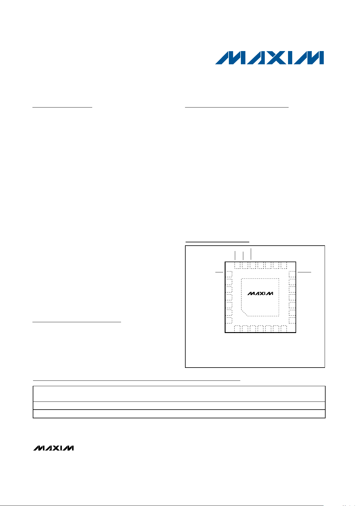
THIN QFN
(4mm x 4mm)
TOP VIEW
Pin Configurations
19-1013; Rev 0; 11/07
For pricing, delivery, and ordering information, please contact Maxim Direct at 1-888-629-4642,
or visit Maxim’s website at www.maxim-ic.com.
Pin Configurations continued at end of data sheet.
PART
MONITORED
VOLTAGES
VOLTAGES
SEQUENCED
PIN-PACKAGE PACKAGE CODE
MAX16050ETI+ 5 4 28 TQFN-EP* T2844-1
MAX16051ETI+ 6 5 28 TQFN-EP* T2844-1
Note: All devices are specified over the -40°C to +85°C operating temperature range.
+
Denotes lead-free package.
*
EP = Exposed pad.
Typical Operating Circuit appears at end of data sheet.
Servers
Workstations
Networking Systems
Telecom Equipment
Storage Systems
MAX16050/MAX16051
Voltage Monitors/Sequencer Circuits with
Reverse-Sequencing Capability
2 _______________________________________________________________________________________
ABSOLUTE MAXIMUM RATINGS
ELECTRICAL CHARACTERISTICS
(V
CC
= 2.7V to 13.2V, VEN= V
ABP
, TA= TJ= -40°C to +85°C, unless otherwise noted. Typical values are at TA= +25°C.) (Note 1)
Stresses beyond those listed under “Absolute Maximum Ratings” may cause permanent damage to the device. These are stress ratings only, and functional
operation of the device at these or any other conditions beyond those indicated in the operational sections of the specifications is not implied. Exposure to
absolute maximum rating conditions for extended periods may affect device reliability.
(All voltages referenced to GND.)
V
CC
.........................................................................-0.3V to +30V
REM, OUT_, DISC_.................................................-0.3V to +30V
RESET, SHDN, SET_, FAULT, EN_HOLD, EN, DELAY,
OV_OUT, ABP, TIMEOUT, SEQ_...........................-0.3V to +6V
CP_OUT.........................................................-0.3V to (V
CC
+ 6V)
RESET Current ....................................................................50mA
DISC_ Current ...................................................................180mA
Input/Output Current (all other pins) ...................................20mA
Continuous Power Dissipation (T
A
= +70°C)
28-Pin (4mm x 4mm) Thin QFN (derate 28.6mW/°C
above +70°C) ............................................................2285mW*
Operating Temperature Range ...........................-40°C to +85°C
Junction Temperature .....................................................+150°C
Storage Temperature Range .............................-65°C to +150°C
Lead Temperature (soldering, 10s) .................................+300°C
*
As per JEDEC51 Standard (Multilayer Board).
PARAMETER SYMBOL CONDITIONS MIN TYP MAX UNITS
Operating Voltage Range
(Note 2)
V
CC
Voltage on VCC to ensure the device is fully
operational
2.7 13.2 V
Operating Voltage V
CCR
V
DISC_
= V
OUT_
= V
RESET
= low, voltage on
V
CC
rising
1.8 V
Regulated Supply Voltage V
ABP
I
ABP
= 1mA (external sourcing current from
ABP)
2.45 2.90 V
Undervoltage Lockout V
UVLO
Minimum voltage on ABP, ABP rising 2.1 2.3 V
Undervoltage Lockout Hysteresis V
UVLO_HYS
ABP falling 100 mV
Supply Current I
CC
VCC = 3.3V, all OUT_ = high, no load 0.7 1.1 mA
MONITORED ANALOG INPUTS
SET_ Threshold V
TH
SET_ falling 0.492 0.5 0.508 V
SET_ Threshold Hysteresis V
TH_HYS
SET_ rising 0.5 %V
TH
SET1–SET4 Input Current I
SET
V
SET_
= 0.5V -100 +100 nA
SET5 Input Current I
SET5
V
SET5
= 0.5V (MAX16051 only) -30 +30 µA
SET_ Threshold Tempco ΔV
TH/_TC
30 ppm/°C
Overvoltage Threshold V
TH_OV
SET_ falling 0.541 0.55 0.558 V
Overvoltage Threshold Hysteresis SET_ rising 0.5 %V
TH_OV
EN Threshold V
TH_EN
EN_ falling 0.492 0.5 0.508 V
EN Threshold Hysteresis V
EN_HYS
EN_ rising 0.5 %V
TH_EN
EN Input Current I
EN
VEN = 0.5V -100 +100 nA
SEQUENCING, CAPACITOR DISCHARGE, AND SEQUENCE TIMING OUTPUTS
VCC = 3.3V, I
SINK
= 3.2mA 0.3
OUT_ Output Low Voltage V
OL_OUT
VCC = 1.8V, I
SINK
= 100µA 0.3
V
OUT_ Leakage Current I
LKG_OUT
V
OUT_
= 12V, OUT_ asserted 1 µA
DISC_ Output Pulldown Current I
OL_DISC
Pulldown current during fault condition or
power-down mode, V
DISC_
= 1V
85 mA
DISC_ Output Leakage Current I
LKG_DISCVDISC_
= 3.3V, not in power-down mode 1 µA
DISC_ Power Low Threshold V
TH_PL
DISC_ falling 200 250 300 mV
MAX16050/MAX16051
Voltage Monitors/Sequencer Circuits with
Reverse-Sequencing Capability
_______________________________________________________________________________________ 3
ELECTRICAL CHARACTERISTICS (continued)
(V
CC
= 2.7V to 13.2V, VEN= V
ABP
, TA= TJ= -40°C to +85°C, unless otherwise noted. Typical values are at TA= +25°C.) (Note 1)
Note 1: Specifications are guaranteed for the stated global conditions, unless otherwise noted. 100% production tested at T
A
=
+25°C and T
A
= +85°C. Specifications at TA= -40°C are guaranteed by design.
Note 2: When the voltage is below the V
UVLO
and above V
CCR
, OUT_ and RESET are asserted low.
Note 3: SEQ1–SEQ3 are inputs with three logic levels: high, low, and high-impedance.
PARAMETER SYMBOL CONDITIONS MIN TYP MAX UNITS
DELAY, TIMEOUT Output Source
Current
I
DT
V
DELAY
= V
TIMEOUT
= 0V 1.7 2.5 3.0 µA
DELAY, TIMEOUT Threshold
Voltage
V
TH_DT
1.218 1.250 1.281 V
DIGITAL INPUTS/OUTPUTS
SHDN, FAULT, EN_HOLD Input-
Logic Low Voltage
V
IL
0.4 V
SHDN, FAULT, EN_HOLD Input-
Logic High Voltage
V
IH
2V
EN_HOLD Input Current I
I
1µA
EN_HOLD to OUT Delay t
EN_OUT
3µs
FAULT, SHDN to ABP Pullup
Resistance
R
P
60 100 160 kΩ
SHDN to OUT_ Delay t
OUT
12 µs
VCC = 3.3V, I
SINK
= 3.2mA 0.3
RESET Output Low Voltage V
OL
VCC = 1.8V, I
SINK
= 100µA 0.3
V
REM, FAULT Output Low Voltage V
OL_RFVCC
= 3.3V, I
SINK
= 3.2mA 0.3 V
FAULT Pulse Width t
FAULT_PW
1.9 µs
SET_ to FAULT Delay Time t
SET_FAULT
SET_ falling below respective threshold 2.5 µs
SEQ1–SEQ3 Logic-High Level V
IH_SEQ
MAX16050 only
V
ABP
-
0.35
V
SEQ1–SEQ3 Logic HighImpedance (No Connect) Level
V
IX_SEQ
MAX16050 only 0.92 1.45 V
SEQ1–SEQ3 Logic-Low Level V
IL_SEQ
MAX16050 only 0.33 V
SEQ1–SEQ3 High-Impedance
State Tolerance Current
I
IX
MAX16050 (Note 3) -6 +6 µA
RESET CIRCUIT
RESET, REM, OV_OUT Output
Leakage
I
LKG
V
RESET
= V
REM
= V
OV_OUT
= 5V 1 µA
RESET Timeout Period t
RP
TIMEOUT = ABP 50 128 300 ms
OUT_, FAULT, SHDN to RESET
Delay
t
RST
TIMEOUT = unconnected 3 µs
CHARGE-PUMP OUTPUT
CP_OUT Voltage V
CP_OUTICP_OUT
= 0.5µA
V
CC
+
4.6
VCC +5VCC +
5.8
V
CP_OUT Source Current I
CP_OUTVCP_OUT
= VCC + 2V 17 25 30 µA
MAX16050/MAX16051
Voltage Monitors/Sequencer Circuits with
Reverse-Sequencing Capability
4 _______________________________________________________________________________________
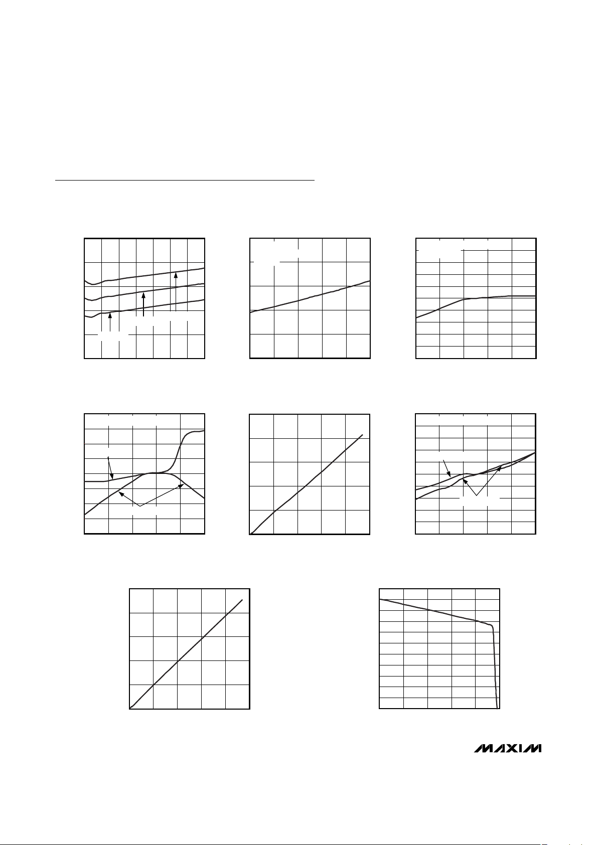
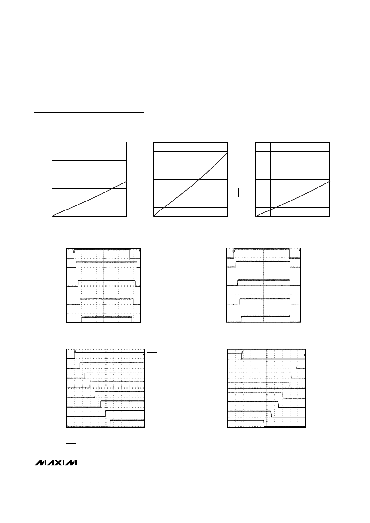
Typical Operating Characteristics
(V
CC
= 5V; VEN= V
ABP
, TA= +25°C, unless otherwise noted.)
SUPPLY CURRENT
vs. SUPPLY VOLTAGE
MAX16050/51 toc01
SUPPLY VOLTAGE (V)
SUPPLY CURRENT (μA)
11.710.28.77.25.74.2
550
600
650
700
750
500
2.7 13.2
TA = -40°C
TA = +85°C
TA = +25°C
SUPPLY CURRENT
vs. TEMPERATURE
MAX16050/51 toc02
TEMPERATURE (°C)
SUPPLY CURRENT (μA)
603510-15
550
600
650
700
750
500
-40 85
VCC = 5V
ALL OUT_ = HIGH
NO LOAD
NORMALIZED SET_ THRESHOLD VOLTAGE
vs. TEMPERATURE
MAX16050/51 toc03
TEMPERATURE (°C)
NORMALIZED SET_ THRESHOLD VOLTAGE
603510-15
0.996
0.997
0.998
0.999
1.000
1.001
1.002
1.003
1.004
1.005
0.995
-40 85
NORMALIZED AT TA = +25°C
V
SET_
FALLING
NORMALIZED SEQUENCE DELAY
vs. TEMPERATURE
MAX16050/51 toc04
TEMPERATURE (°C)
NORMALIZED SEQUENCE DELAY
6035-15 10
0.85
0.90
0.95
1.00
1.10
1.05
1.15
1.20
0.80
-40 85
NORMALIZED AT TA = +25°C
C
DELAY
= OPEN
C
DELAY
= 0.1μF
SEQUENCE DELAY vs. C
DELAY
MAX16050/51 toc05
C
DELAY
(nF)
SEQUENCE DELAY (ms)
400300200100
50
100
150
200
250
0
0 500
NORMALIZED RESET TIMEOUT PERIOD
vs. TEMPERATURE
MAX16050/51 toc06
TEMPERATURE (°C)
NORMALIZED RESET TIMEOUT PERIOD
603510-15
0.92
0.94
0.96
0.98
1.00
1.02
1.04
1.06
1.08
1.10
0.90
-40 85
NORMALIZED AT TA = +25°C
TIMEOUT = OPEN
TIMEOUT = ABP
RESET TIMEOUT PERIOD
vs. C
TIMEOUT
MAX16050/51 toc07
C
TIMEOUT
(nF)
RESET TIMEOUT PERIOD (ms)
400300200100
50
100
150
200
250
0
0500
CP_OUT VOLTAGE
vs. CP_OUT CURRENT
MAX16050/51 toc08
CP_OUT CURRENT (μA)
CP_OUT VOLTAGE (V)
2015105
1
2
3
4
5
6
7
8
9
10
11
0
025
MAX16050/MAX16051
Voltage Monitors/Sequencer Circuits with
Reverse-Sequencing Capability
_______________________________________________________________________________________
5
Typical Operating Characteristics (continued)
(V
CC
= 5V; VEN= V
ABP
, TA= +25°C, unless otherwise noted.)
OV_OUT LOW VOLTAGE
vs. SINK CURRENT
MAX16050/51 toc09
SINK CURRENT (mA)
OV_OUT LOW VOLTAGE (V)
16124 8
0.1
0.2
0.3
0.4
0.6
0.5
0.7
0.8
0
020
OUT_ LOW VOLTAGE
vs. SINK CURRENT
MAX16050/51 toc10
SINK CURRENT (mA)
OUT_ LOW VOLTAGE (V)
16124 8
0.1
0.2
0.3
0.4
0.6
0.5
0.7
0.8
0
020
RESET LOW VOLTAGE
vs. SINK CURRENT
MAX16050/51 toc11
SINK CURRENT (mA)
RESET LOW VOLTAGE (V)
16124 8
0.1
0.2
0.3
0.4
0.6
0.5
0.7
0.8
0
020
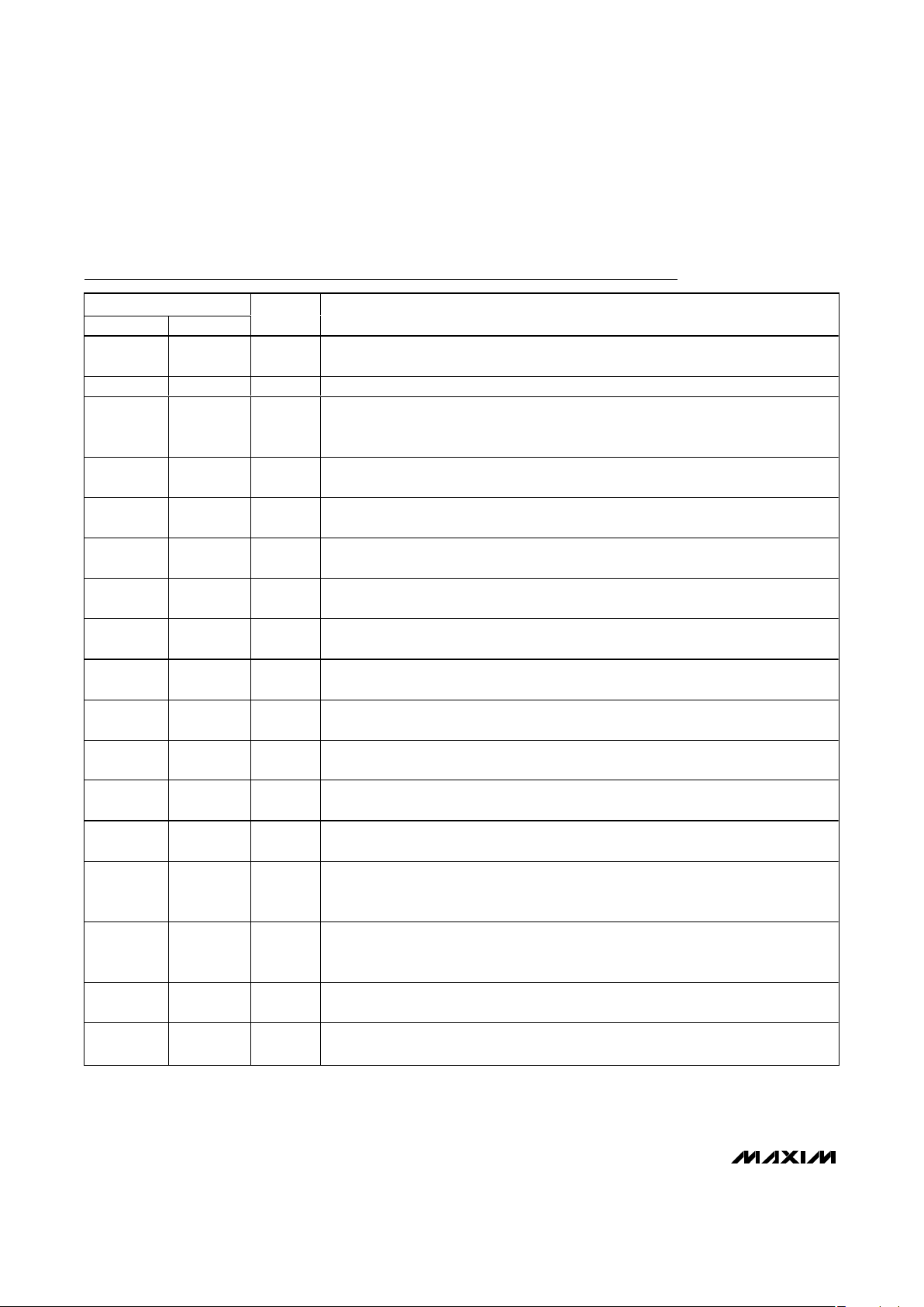
REVERSE SEQUENCE POWER-DOWN USING SHDN
(C
DELAY
= C
TIMEOUT
= OPEN)
MAX1650/51 toc12
40μs/div
SHDN
5V/div
V1
5V/div
V2
5V/div
V3
5V/div
V4
5V/div
SIMULTANEOUS POWER-DOWN USING EN
(C
DELAY
= C
TIMEOUT
= OPEN)
MAX1650/51 toc13
40μs/div
EN
5V/div
V1
5V/div
V2
5V/div
V3
5V/div
V4
5V/div
DAISY-CHAINING TWO DEVICES
WITH SHDN RISING (FIGURE 7)
MAX1650/51 toc14a
100μs/div
C
DELAY
(U1) = C
DELAY
(U2) = 100pF
SHDN = 5V/div
V1–V7 = 5V/div
SHDN
V1
V2
V3
V7
V6
V5
V4
DAISY-CHAINING TWO DEVICES
WITH SHDN FALLING (FIGURE 7)
MAX1650/51 toc14b
10μs/div
C
DELAY
(U1) = C
DELAY
(U2) = 100pF
SHDN = 5V/div
V1–V7 = 5V/div
SHDN
V1
V2
V3
V7
V6
V5
V4
MAX16050/MAX16051
Voltage Monitors/Sequencer Circuits with
Reverse-Sequencing Capability
6 _______________________________________________________________________________________
Pin Description
PIN
MAX16050 MAX16051
NAME FUNCTION
11V
CC
Device Power-Supply Input. Connect to 2.7V to 13.2V. Bypass VCC to GND with a 0.1µF
capacitor.
2 2 GND Ground
3 3 ABP
Internal Supply Bypass Input. Connect a 1µF capacitor from ABP to GND. ABP is an
internally generated voltage and must not be used to supply more than 1mA to external
circuitry.
44EN
Analog Enable Input. Connect a resistive divider at EN to monitor a voltage. The EN
threshold is 0.5V.
5 5 SET4
Set Monitored Threshold 4 Input. Monitor a voltage by setting the threshold with an
external resistive divider. The SET4 threshold is 0.5V.
6 6 OUT4
Open-Drain Output 4. When the voltage at SET3* is above 0.5V, OUT4 goes high
impedance. OUT4 requires an external pullup resistor and can be pulled up to 13.2V.
7 7 DISC4
Discharge Pulldown Input 4. During normal operation, DISC4 is high impedance. During a
fault condition or power-down, DISC4 provides an 85mA sink current.
8 8 SET3
Set Monitored Threshold 3 Input. Monitor a voltage by setting the threshold with an
external resistive divider. The SET3 threshold is 0.5V.
9 9 OUT3
Open-Drain Output 3. When the voltage at SET2* is above 0.5V, OUT3 goes high
impedance. OUT3 requires an external pullup resistor and can be pulled up to 13.2V.
10 10 DISC3
Discharge Pulldown Input 3. During normal operation, DISC3 is high impedance. During a
fault condition or power-down, DISC3 provides an 85mA sink current.
11 11 SET2
Set Monitored Threshold 2 Input. Monitor a voltage by setting the threshold with an
external resistive divider. The SET2 threshold is 0.5V.
12 12 OUT2
Open-Drain Output 2. When the voltage at SET1* is above 0.5V, OUT2 goes high
impedance. OUT2 requires an external pullup resistor and can be pulled up to 13.2V.
13 13 DISC2
Discharge Pulldown Input 2. During normal operation, DISC2 is high impedance. During a
fault condition or power-down, DISC2 provides an 85mA sink current.
14 14 EN_HOLD
Enable Hold Input. When EN_HOLD is low, the device does not start the reversesequencing process regardless of the status of the SHDN input. Reverse sequencing is
allowed when this input is pulled high. Connect to ABP if unused.
15 15 REM
Open-Drain Bus Removal Output. REM goes high impedance when all DISC_ inputs are
below the DISC_ power low threshold (V
TH_PL
). REM goes low when any DISC_ input goes
above V
TH_PL
. REM requires an external pullup resistor and can be pulled up to 13.2V.
16 16 DISC1
Discharge Pulldown Input 1. During normal operation, DISC1 is high impedance. During a
fault condition or power-down, DISC1 provides an 85mA sink current.
17 17 OUT1
Open-Drain Output 1. When the voltage at EN* is above 0.5V, OUT1 goes high
impedance. OUT1 requires an external pullup resistor and can be pulled up to 13.2V.
*
This applies to the MAX16051. For the MAX16050, see Table 1 for the output sequence order.
MAX16050/MAX16051
Voltage Monitors/Sequencer Circuits with
Reverse-Sequencing Capability
_______________________________________________________________________________________ 7
Pin Description (continued)
PIN
MAX16050 MAX16051
NAME FUNCTION
18 18 SET1
Set Monitored Threshold 1 Input. Monitor a voltage by setting the threshold with an
external resistive divider. The SET1 threshold is 0.5V.
19 19 OV_OUT
Open-Drain Overvoltage Output. When any of the SET_ voltages exceed their 0.55V
overvoltage threshold, OV_OUT goes low. When all of the SET_ voltages are below their
overvoltage threshold, OV_OUT goes high impedance after a short propagation delay.
20 20 RESET
Open-Drain Reset Output. When any of the monitored voltages (including EN) falls below
its threshold, SHDN is pulled low, or FAULT is pulled low, RESET asserts and stays
asserted for at least the minimum reset timeout period after all of these conditions are
removed. The reset timeout is 128ms (typ) when TIMEOUT is connected to ABP or can be
adjusted by connecting a capacitor from TIMEOUT to GND.
21 21 FAULT
FAULT Synchronization Input/Output. While EN = SHDN = high, FAULT is pulled low when
any of the SET_ voltages falls below their respective threshold. Pull FAULT low manually to
assert a simultaneous power-down. FAULT is internally pulled up to ABP by a 100kΩ
resistor.
22 22 SHDN
Active-Low Shutdown Input. When SHDN is pulled low, the device will reverse sequence
for power-down operation. SHDN is internally pulled up to ABP by a 100kΩ resistor.
23 23 DELAY
Adjustable Sequence Delay Timing Input. Connect a capacitor from DELAY to GND to set
the sequence delay between each OUT_. Leave DELAY unconnected for a 10µs (typ)
delay.
24 24 TIMEOUT
Adjustable Reset Timeout Input. Connect a capacitor from TIMEOUT to GND to set the
reset timeout period. Connect TIMEOUT to ABP for the fixed timeout of 128ms (typ). Leave
TIMEOUT unconnected for a 10µs (typ) delay.
25 — SEQ1
26 — SEQ2
27 — SEQ3
Sequence Order Select Inputs. SEQ1, SEQ2, and SEQ3 allow the order of sequencing for
each supply to be programmable (Table 1).
28 28 CP_OUT
Charge-Pump Output. An internal charge pump boosts CP_OUT to (V
CC
+ 5V ) to provide
a pullup voltage that can be used to drive external n-channel MOSFETs. CP_OUT sources
up to 25µA.
— 25 DISC5
Discharge Pulldown Input 5. During normal operation, DISC5 is high impedance. During a
fault condition or power-down, DISC5 provides an 85mA sink current.
— 26 OUT5
Open-Drain Output 5. When the voltage at SET4 is above 0.5V, OUT5 goes high
impedance. OUT5 requires an external pullup resistor and can be pulled up to 13.2V.
— 27 SET5
External Set Monitored Threshold 5. Monitor a voltage by setting the threshold with an
external resistive divider. The SET5 threshold is 0.5V.
——EP
Exposed Pad. EP is internally connected to GND. Connect EP to the GND plane for
improved heat dissipation. Do not use EP as the only ground connection.

MAX16050/MAX16051
Voltage Monitors/Sequencer Circuits with
Reverse-Sequencing Capability
8 _______________________________________________________________________________________
Functional Diagram
MAX16050
MAX16051
RESET
ABP
OUT1–OUT4
(OUT1–OUT5)
DISC1–DISC4
(DISC1–DISC5)
INTERNAL
V
CC
/UVLO
V
CC
CONTROL
LOGIC
CHARGE
PUMP
CP_OUT
SET1–SET4
(SET1–SET5)
EN
GND
DELAY
TIMEOUT
COMP
V
REF
COMP
COMP
EN_HOLD
( ) ARE FOR MAX16051 ONLY.
SEQ1–SEQ3
(MAX16050 ONLY)
250mV
85mA
OV_OUT
REM
ABP
FAULT
ABP

MAX16050/MAX16051
t
DELAY
t
DELAY
t
DELAY
t
DELAY
V1
V3
V2
V4
V
TH_EN
V
TH
V
TH
V
TH
V
TH
EN
REM
t
RP
V
TH_PL
SHDN
RESET
Figure 1. Sequencing Timing Diagram with Reverse Order Power-Down Using SHDN
Voltage Monitors/Sequencer Circuits with
Reverse-Sequencing Capability
_______________________________________________________________________________________ 9

MAX16050/MAX16051
Voltage Monitors/Sequencer Circuits with
Reverse-Sequencing Capability
10 ______________________________________________________________________________________
t
DELAY
t
DELAY
V
TH_EN
V
TH_EN
V
TH
t
RP
V
TH_PL
SHDN
RESET
V
TH
V
TH
V
TH
t
DELAY
t
DELAY
V1
V3
V2
V4
EN
REM
Figure 2. Sequencing Timing Diagram with Simultaneous Order Power-Down Using EN

MAX16050/MAX16051
V
TH_PL
RESET
t
DELAY
V
TH_PL
V1
V3
V2
V4
REM
FAULT
t
FAULT-PW
Figure 3. Sequencing Timing Diagram During a System Fault
Voltage Monitors/Sequencer Circuits with
Reverse-Sequencing Capability
______________________________________________________________________________________ 11

MAX16050/MAX16051
Voltage Monitors/Sequencer Circuits with
Reverse-Sequencing Capability
12 ______________________________________________________________________________________
V1
V3
V2
EN
V4
PART DOES NOT RESPOND TO EN FALLING...
...
UNTIL EN_HOLD GOES HIGH
CONNECTED TO REM OF THE SECOND IC
EN_HOLD
Figure 4. Power-Down Characteristics when REM of the Second IC is Connected to EN_HOLD of the First IC

MAX16050/MAX16051
Detailed Description
The MAX16050 monitors up to 5 voltages (Figure 5) with
the ability to sequence up to 4 voltages, while the
MAX16051 monitors up to 6 voltages with the ability to
sequence up to 5 voltages. These devices control system power-up and power-down in a particular
sequence order. The MAX16050/MAX16051 turn off all
supplies and assert a reset to the processor when any
of the voltages falls below its respective threshold. The
MAX16050/MAX16051 offer an 85mA pulldown feature
that helps discharge the output capacitance of DC-DC
converters to ensure timely power-down. In addition, the
MAX16050/MAX16051 also reverse sequence, monitoring each power-supply output voltage present at the
associated DISC_ input and ensuring that the voltage
falls below 250mV before turning off the next supply.
The MAX16050 provides three sequence logic inputs,
which select the sequence order from 24 possible
combinations (Table 1). In the default mode (SEQ1 =
SEQ2 = SEQ3 = High Impedance), the power-up
sequence is OUT1→OUT2→OUT3→OUT4. The
MAX16051 features an additional channel and the
sequence order is fixed at OUT1→OUT2→OUT3
→OUT4→OUT5. For complex systems with a large
number of power supplies, the MAX16050/MAX16051
can be used in a daisy-chain configuration. Reverse
sequencing in the daisy-chained configuration is still
possible.
The MAX16050/MAX16051 keep all OUT_ low (all of the
supplies in the off-state) until four conditions are met.
1) The voltage at ABP exceeds the undervoltage lockout threshold.
2) The voltage at the analog enable input (EN) is
above its threshold.
3) The shutdown input, SHDN, is not asserted.
4) All DISC_ voltages must be below 250mV.
OUT1
GND
ON
OFF
SHDN
MAX16050
SET1
DISC1
OUT2
SET2
DISC2
OUT3
SET3
DISC3
OUT4
SET4
DISC4
V
BUS
V
PU
V1
RESET
OV_OUT
FAULT
REM
EN
V
CC
EN_HOLD
ABP
SEQ1
CP_OUT
SEQ2
SEQ3
TIMEOUT
DELAY
V2
V3
DC-DC
EN
DC-DC
EN
DC-DC
EN
DC-DC
EN
V4
Figure 5. Typical Connection for Sequencing Four DC-DC Converters
Voltage Monitors/Sequencer Circuits with
Reverse-Sequencing Capability
______________________________________________________________________________________ 13

MAX16050/MAX16051
Voltage Monitors/Sequencer Circuits with
Reverse-Sequencing Capability
14 ______________________________________________________________________________________
When all of these conditions are met, the device starts
the power-sequencing process by turning on
OUT1–OUT_ in the sequence order. The sequence
delay between each OUT_ is the time required for the
power-supply voltage to exceed the undervoltage
threshold plus the additional time delay set by the
external delay capacitor; if no capacitor is connected to
the sequence delay timing input (DELAY), only a short
propagation delay (10µs) occurs. As each voltage
meets its respective threshold, the next OUT_ in the
sequence goes high impedance (open-drain output),
allowing the next power supply to turn on, which is then
monitored by the next input stage. When all of the voltages exceed their respective thresholds, the reset output (RESET) deasserts after a reset timeout period to
allow the system controller to start operating.
After sequencing is complete, if any SET_ input drops
below its threshold, a fault is detected. All power supplies are simultaneously turned off by the OUT_ outputs
asserting low, the RESET output asserting, the DISC_
current pulldown turning on, and the FAULT output
pulling low for at least 1.9µs. The MAX16050/MAX16051
will then be ready to power on again. Sequencing
begins as soon as the four startup conditions are met.
Sequencing
The MAX16050 features three three-state sequence
logic inputs that select one of the 24 possible
sequence orders (Table 1). These inputs allow the
sequence order to be changed even after the board
layout is finalized. The MAX16051 offers five channels
and the device powers up in a fixed order from OUT1
to OUT5.
SEQUENCE ORDER
SEQ1 SEQ2 SEQ3
FIRST SUPPLY
SECOND SUPPLY THIRD SUPPY
FOURTH SUPPLY
High-Z High-Z High-Z OUT1 OUT2 OUT3 OUT4
High-Z High-Z Low OUT1 OUT2 OUT4 OUT3
High-Z High-Z High OUT1 OUT3 OUT2 OUT4
High-Z Low High-Z OUT1 OUT3 OUT4 OUT2
High-Z Low Low OUT1 OUT4 OUT2 OUT3
High-Z Low High OUT1 OUT4 OUT3 OUT2
High-Z High High-Z OUT2 OUT1 OUT3 OUT4
High-Z High Low OUT2 OUT1 OUT4 OUT3
High-Z High High OUT2 OUT3 OUT1 OUT4
Low High-Z High-Z OUT2 OUT3 OUT4 OUT1
Low High-Z Low OUT2 OUT4 OUT1 OUT3
Low High-Z High OUT2 OUT4 OUT3 OUT1
Low Low High-Z OUT3 OUT1 OUT2 OUT4
Low Low Low OUT3 OUT1 OUT4 OUT2
Low Low High OUT3 OUT2 OUT1 OUT4
Low High High-Z OUT3 OUT2 OUT4 OUT1
Low High Low OUT3 OUT4 OUT1 OUT2
Low High High OUT3 OUT4 OUT2 OUT1
High High-Z High-Z OUT4 OUT1 OUT2 OUT3
High High-Z Low OUT4 OUT1 OUT3 OUT2
High High-Z High OUT4 OUT2 OUT1 OUT3
High Low High-Z OUT4 OUT2 OUT3 OUT1
High Low Low OUT4 OUT3 OUT1 OUT2
High Low High OUT4 OUT3 OUT2 OUT1
Table 1. MAX16050 Sequencing Table Logic

MAX16050/MAX16051
Charge-Pump Output (CP_OUT)
The MAX16050/MAX16051 feature an on-chip charge
pump that drives its output voltage to 5V above V
CC
,
and it can be used as a pullup voltage to drive one or
more external n-channel MOSFETs (see the
Typical
Operating Circuit
). The charge-pump output can be
modeled as a 25µA current source with a compliance
voltage of (VCC+ 5V); the slew rate can be controlled
by connecting a capacitor from the gate of the MOSFET
to ground. When using CP_OUT to provide the pullup
voltage for multiple MOSFETs, ensure that the voltage
is enough to enhance a MOSFET despite the load of
the other pullup resistors (which may be connected to
outputs that are deasserted low).
Disabling Channels
If any channel is not used, connect the associated SET_
input to another SET_ input that is previous to the disabled channel in the sequence order. Connect DISC_ of
the disabled channel to GND or leave it unconnected.
The channel exclusion feature adds more flexibility to
the device in a variety of different applications.
SHDN
and EN Inputs
The shutdown input (SHDN) initiates a reverse
sequencing event. When SHDN is brought low, the
device will sequentially power down in reverse order.
During this period, all DISC_ inputs are monitored to
make sure the voltage of each supply falls below
250mV before allowing the next supply to shut down.
The next OUT_ goes low as soon as the previous DISC_
input drops below 250mV without any capacitor-adjusted delay. This continues until all supplies are turned off.
SHDN is internally pulled up to ABP.
When EN falls below its threshold, the device performs
a simultaneous power-down and does not reverse
sequence. When either SHDN or EN initializes the
power-down event, the reset output (RESET) immediately asserts. At the end of the power-down event,
when all DISC_ voltages are below 250mV, the bus
removal output (REM) goes high impedance.
Reset Output (
RESET
)
The MAX16050/MAX16051 include a reset output.
RESET is an open-drain output and requires an external
pullup resistor.
When any of the monitored voltages falls below its
threshold, SHDN is pulled low, EN falls below its threshold, or FAULT is pulled low, RESET asserts and stays
asserted for at least the minimum reset timeout period
after all of these conditions are removed. Connect a
capacitor from TIMEOUT to GND to adjust the reset
timeout period. Connect TIMEOUT to ABP for the fixed
timeout of 128ms (typ). Leave TIMEOUT unconnected
for a 10µs (typ) timeout period.
FAULT
Input/Output
The FAULT input/output asserts to signal a fault if any of
the SET_ monitored voltages falls below its threshold
while EN = SHDN = high. FAULT is internally pulled up
to ABP by a 100kΩ resistor. FAULT also can be used as
an input. Pull FAULT low to simultaneously shut down
the OUT_ outputs .
For multichip solutions, all of the FAULT input/outputs
can be connected together. In case of a fault condition,
all outputs on every device are turned off and the internal pulldown circuitry is activated simultaneously.
Overvoltage Fault Output (
OV_OUT
)
The MAX16050/MAX16051 include an overvoltage fault
output. OV_OUT is an open-drain output and requires
an external pullup resistor. When any of the SET_ voltages exceed their 0.55V overvoltage threshold,
OV_OUT goes low. When all of the SET_ voltages are
below their overvoltage threshold, OV_OUT goes high
impedance after a short propagation delay.
Discharge Inputs (DISC_)
The discharge inputs (DISC_) discharge power-supply
capacitors during a power-down or fault event and monitor power-supply output voltages during reverse
sequencing. When an OUT_ output goes low, the associated DISC_ activates an 85mA pulldown current to discharge any output capacitors. This helps the
power-supply output drop below the 250mV level so the
next power supply can be turned off. During normal
operation, DISC_ is high impedance and will not load
the circuit.
Bus Removal Output (REM)
The MAX16050/MAX16051 include an open-drain bus
removal output (REM) that indicates when it is safe to
disconnect the input power after a controlled powerdown operation. REM monitors DISC_ voltages and
goes low when any DISC_ input voltage goes above the
DISC_ power low threshold (V
TH_PL
). REM goes high
when all DISC_ inputs are below the DISC_ power low
threshold (V
TH_PL
). For a visual signal of when it is
unsafe to remove a powered board from the bus, connect an LED to REM.
Voltage Monitors/Sequencer Circuits with
Reverse-Sequencing Capability
______________________________________________________________________________________ 15

Enable Hold Input (
EN_HOLD
)
When EN_HOLD is low, a high-to-low transition on
SHDN or on EN is ignored. EN_HOLD must be high for
SHDN or EN to disable the device. This feature is used
when multiple MAX16050/MAX16051s are daisychained (see Figure 7). Connect EN_HOLD to ABP if
not used.
Delay Time Input (DELAY)
Connect a capacitor (C
DELAY
) between DELAY and
GND to adjust the sequencing delay period (t
DELAY
)
that occurs between sequenced channels. Use the following formula to estimate the delay:
t
DELAY
= 10µs + (500kΩ x C
DELAY
)
where t
DELAY
is in seconds and C
DELAY
is in Farads.
Leave DELAY unconnected for the default 10µs (typ)
delay.
Reset Timeout Input (TIMEOUT)
Connect a capacitor (C
TIMEOUT
) from TIMEOUT to
GND to set the reset timeout period. After all SET_
inputs exceed their thresholds (VTH), RESET remains
low for the programmed timeout period, tRP, before
deasserting (see Figure 1). Use the following formula to
estimate the reset timeout period:
tRP= 10µs + (500kΩ x C
TIMEOUT
)
where tRPis in seconds and C
TIMEOUT
is in Farads.
Leave TIMEOUT unconnected for the default 10µs (typ)
timeout delay or connect TIMEOUT to ABP to enable a
fixed 128ms (typ) timeout.
Applications Information
Resistor Value Selection
The MAX16050/MAX16051 feature four and five SET_
inputs, respectively, and the threshold voltage (VTH) at
each SET_ input is 0.5V (typ). To monitor a voltage
V
1TH
, connect a resistive divider network to the circuit
as shown in Figure 6, and use the following equation to
calculate the monitored threshold voltage:
Balance accuracy and power dissipation when choosing the external resistors. The input to the voltage monitor is a high-impedance input with a small 100nA
leakage current. This leakage current contributes to the
overall error of the threshold voltage, and this error is
proportional to the value of the resistors used to set the
threshold. Small-valued resistors reduce the error but
increase the power consumption. Use the following
equation to estimate the value of the resistors based on
the amount of acceptable error:
where e
A
is the fraction of the maximum acceptable
absolute resistive divider error attributable to the input
leakage current (use 0.01 for ±1%), V
1TH
is the powergood threshold for the power supply being monitored,
and I
SET
is the worst-case SET_ input leakage current
(see the
Electrical Characteristics
table). Calculate R2
as follows:
Pullup Resistor Values
The exact value of the pullup resistors for the opendrain outputs is not critical, but some consideration
should be made to ensure the proper logic levels when
the device is sinking current. For example, if VCC=
3.3V and the pullup voltage is 5V, keep the sink current
less than 3.2mA as shown in the
Electrical
Characteristics
table. As a result, the pullup resistor
should be greater than 1.6kΩ. For a 13.2V pullup, the
resistor should be larger than 4.1kΩ.
Extra care must be taken when using CP_OUT as the
pullup voltage. If multiple pullup resistors are connected to CP_OUT and one or more of the connected OUT_
outputs are asserted, the current drawn can drop the
CP_OUT voltage enough to prevent an enabled
MOSFET from turning on completely.
R
VR
VV
2
TH 1
1TH TH
=
×
−
R
eV
I
1
A 1TH
SET
=
×
VV1
R1
R2
1TH TH
=×+
⎛
⎝
⎜
⎞
⎠
⎟
MAX16050
MAX16051
SET_
V
CC
GND
V
BUS
RESET
V
1TH
R1
R2
Figure 6. Setting the SET_ Input
MAX16050/MAX16051
Voltage Monitors/Sequencer Circuits with
Reverse-Sequencing Capability
16 ______________________________________________________________________________________

MAX16050/MAX16051
Daisy-Chaining the MAX16050/MAX16051
The MAX16050/MAX16051 can be daisy-chained to
sequence and monitor a large number of voltages
(Figure 7). When a fault occurs on any of the monitored
inputs, FAULT goes low, signaling a fast power-down.
Connect all FAULT pins of the MAX16050/MAX16051
together to ensure that all power supplies are turned off
during a fault.
In Figure 7, SHDN is pulled low to initiate the powerdown sequence. When all of the supply voltages monitored by U2 are off, the bus removal output (REM) goes
high, thereby allowing U1 to start sequencing down.
REM normally is at a logic-low state when all voltages
are good. Connect U2’s REM to U1’s EN_HOLD to
force U1 to stay on even if EN and SHDN are pulled
low. This enable-and-hold circuitry allows the system to
power down correctly.
MOSFET Selection
The external pass MOSFET connects in series with the
sequenced power-supply source. Since the load current and the MOSFET drain-to-source impedance
(R
DSON
) determine the voltage drop, the on-characteristics of the MOSFET affect the load supply accuracy.
For highest supply accuracy and lowest voltage drop,
select a MOSFET with an appropriate drain-to-source
on-resistance with a gate-to-source bias of 4.5V to 6.0V
(see Table 2).
Layout and Bypassing
For better noise immunity, bypass VCCto GND with a
0.1µF capacitor installed as close to the device as possible. Bypass ABP to GND with a 1µF capacitor
installed as close to the device as possible; ABP is an
internally generated voltage and must not be used to
supply more than 1mA to external circuitry. Connect the
exposed pad (EP) to the ground plane for improved
heat dissipation. Do not use EP as the only ground connection for the device.
Voltage Monitors/Sequencer Circuits with
Reverse-Sequencing Capability
______________________________________________________________________________________ 17
MANUFACTURER PART
V
DS
(V)
V
GSth
(V)
R
DSON
AT V
GS
= 4.5V
(mΩ)
I
MAX
AT 50mV
VOLTAGE DROP (A)
Qg (nC)
(TYP)
FOOTPRINT
FDC633N 30 0.67 42 1.19 11
Super
SOT
TM
-6
FDP8030L
FDB8030L
30 1.5 4.5 11.11 120
TO-220
TO-263AB
FDD6672A 30 1.2 9.5 5.26 33 TO-252
Fairchild
FDS8876 30
2.5
(max)
17 2.94 15 SO-8
Si7136DP 20 3 4.5 11.11 24.5 SO-8
Si4872DY 30 1 10 5 27 SO-8
SUD50N02-09P 20 3 17 2.94 10.5 TO-252
Vishay
Si1488DH 20 0.95 49 1.02 6
SOT-363
SC70-6
IRL3716 20 3 4.8 10.4 53
TO220AB
D2PAK
TO-262
IRL3402 20 0.7 10 5 78 (max) TO-220AB
IRL3715Z 20 2.1 15.5 3.22 7
TO220AB
D2PAK
TO-262
International
Rectifier
IRLML2502 20 1.2 45 1.11 8
SOT23-3
Micro3
TM
Table 2. Recommended MOSFETs

MAX16050/MAX16051
Voltage Monitors/Sequencer Circuits with
Reverse-Sequencing Capability
18 ______________________________________________________________________________________
OUT1
GND
ABP
PULL SHDN LOW TO
INITIATE A REVERSE
ORDER SHUTDOWN
OF ALL 8 SUPPLIES
EN_HOLD
SHDN
CP_OUT
MAX16050
U1
SET1
DISC1
OUT2
SET2
DISC2
OUT3
SET3
DISC3
OUT4
SET4
DISC4
V
BUS
V1
V2
RESET
OV_OUT
FAULT
EN
V
CC
REM
SEQ1
SEQ2
SEQ3
TIMEOUT
DELAY
DC-DC
EN
V3
V4
DC-DC
EN
DC-DC
EN
DC-DC
EN
OUT1
GND
ABP
EN_HOLD
SHDN
CP_OUT
V
PU
MAX16050
U2
SET1
DISC1
OUT2
SET2
DISC2
OUT3
SET3
DISC3
OUT4
SET4
DISC4
V
BUS
V5
V6
RESET
OV_OUT
FAULT
EN
V
CC
REM
SEQ1
SEQ2
SEQ3
TIMEOUT
DELAY
DC-DC
EN
V7
V8
DC-DC
EN
DC-DC
EN
DC-DC
EN
Figure 7. Daisy-Chaining Two Devices to Sequence Up to 8 Voltages

MAX16050/MAX16051
OUT1
GND
ON
OFF
SHDN
CP_OUT
MAX16050
SET1
DISC1
OUT2
SET2
DISC2
OUT3
SET3
DISC3
OUT4
SET4
DISC4
V
BUS
V
PU
V4
V1
RESET
OV_OUT
FAULT
REM
EN
V
CC
EN_HOLD
ABP
SEQ1
SEQ2
SEQ3
TIMEOUT
DELAY
V2
V3
DC-DC
EN
DC-DC
EN
DC-DC
EN
Typical Operating Circuit
Voltage Monitors/Sequencer Circuits with
Reverse-Sequencing Capability
______________________________________________________________________________________ 19

MAX16050/MAX16051
Voltage Monitors/Sequencer Circuits with
Reverse-Sequencing Capability
20 ______________________________________________________________________________________
Chip Information
PROCESS: BiCMOS
TOP VIEW
26
27
25
24
10
+
9
11
GND
EN
SET4
OUT4
DISC4
12
V
CC
RESET
SET1
OUT1
FAULT
DISC1
REM
1
*EP = EXPOSED PAD
2
DISC5
4567
2021 19 17 16 15
OUT5
SET5
OUT2
SET2
DISC3
OUT3
MAX16051
ABP
OV_OUT
3
18
28
8
CP_OUT
SET3
TIMEOUT
23
13
DISC2
DELAY
22
14
EN_HOLD
SHDN
THIN QFN
(4mm x 4mm)
*EP
Pin Configurations (continued)

MAX16050/MAX16051
Voltage Monitors/Sequencer Circuits with
Reverse-Sequencing Capability
______________________________________________________________________________________ 21
Package Information
(The package drawing(s) in this data sheet may not reflect the most current specifications. For the latest package outline information
go to www.maxim-ic.com/packages
.)
24L QFN THIN.EPS

MAX16050/MAX16051
Voltage Monitors/Sequencer Circuits with
Reverse-Sequencing Capability
Maxim cannot assume responsibility for use of any circuitry other than circuitry entirely embodied in a Maxim product. No circuit patent licenses are
implied. Maxim reserves the right to change the circuitry and specifications without notice at any time.
22
____________________Maxim Integrated Products, 120 San Gabriel Drive, Sunnyvale, CA 94086 408-737-7600
© 2007 Maxim Integrated Products is a registered trademark of Maxim Integrated Products, Inc.
Package Information (continued)
(The package drawing(s) in this data sheet may not reflect the most current specifications. For the latest package outline information
go to www.maxim-ic.com/packages
.)
Maxim cannot assume responsibility for use of any circuitry other than circuitry entirely embodied in a Maxim product. No circuit patent licenses are
implied. Maxim reserves the right to change the circuitry and specifications without notice at any time.
22
____________________Maxim Integrated Products, 120 San Gabriel Drive, Sunnyvale, CA 94086 408-737-7600
© 2007 Maxim Integrated Products is a registered trademark of Maxim Integrated Products, Inc.
 Loading...