

19-1085; Rev 1; 10/96
Dual-Channel CardBus and PCMCIA
Power Switches with SMBus™ Serial Interface
________________General Description
The MAX1601/MAX1604 DC power-switching ICs contain a network of low-resistance MOSFET switches that
deliver selectable VCC and VPP voltages to two
CardBus or PC Card host sockets. Key features include
ultra-low-resistance switches, small packaging, softswitching action, and compliance with PCMCIA specifications for 3V/5V switching. 3.3V-only power switching
for fast, 32-bit CardBus applications is supported in two
ways: stiff, low-resistance 3.3V switches allow high 3.3V
load currents (up to 1A); and completely independent
internal charge pumps let the 3.3V switch operate normally, even if the +5V and +12V supplies are disconnected or turned off to conserve power. The internal
charge pumps are regulating types that draw reduced
input current when the VCC switches are static. Also,
power consumption is automatically reduced to 10µA
max when the switches are programmed to high-Z or
GND states over the serial interface, unlike other solutions that may require a separate shutdown-control
input.
Other key features include guaranteed specifications for
output current limit level, and guaranteed specifications
for output rise/fall times (in compliance with PCMCIA
specifications). Reliability is enhanced by thermal-overload protection, accurate current limiting, an overcurrent-fault flag output, undervoltage lockout, and extra
ESD protection at the VCC/VPP outputs. The SMBus serial interface is flexible, and can tolerate logic input levels
in excess of the positive supply rail.
The MAX1604 and MAX1601 are identical, except
for the MAX1604’s VY switch, which has roughly threetimes the on-resistance (typically 140mΩ).The
MAX1601/MAX1604 fit two complete CardBus/PCMCIA
switches into a space-saving, narrow (0.2in. or 5mm
wide) SSOP package.
________________________Applications
Desktop Computers Data Loggers
Notebook Computers Digital Cameras
Docking Stations Printers
Handy-Terminals PCMCIA Read/Write Drives
____________________________Features
♦ Supports Two CardBus Sockets
♦ 1A, 0.08Ω Max VY VCC Switch (MAX1601 only)
1A, 0.14Ω Max VX VCC Switch
♦ Soft Switching for Low Inrush Surge Current
♦ Overcurrent Protection
♦ Overcurrent/Thermal-Fault Flag Output
♦ Thermal Shutdown at T
= +150°C
j
♦ Independent Internal Charge Pumps
♦ Break-Before-Make Switching Action
♦ 10µA Max Standby Supply Current
♦ 5V and 12V Not Required for Low-R
DS(ON)
3.3V
Switching
♦ Complies with PCMCIA 3V/5V Switching
Specifications
♦ Super-Small, 28-Pin SSOP Package
(0.2in. or 5mm wide)
♦ System Management Bus (SMBus) Serial
Interface
_______________Ordering Information
PART
MAX1601EAI
MAX1604EAI
TEMP. RANGE PIN-PACKAGE
-40°C to +85°C
-40°C to +85°C
28 SSOP
28 SSOP
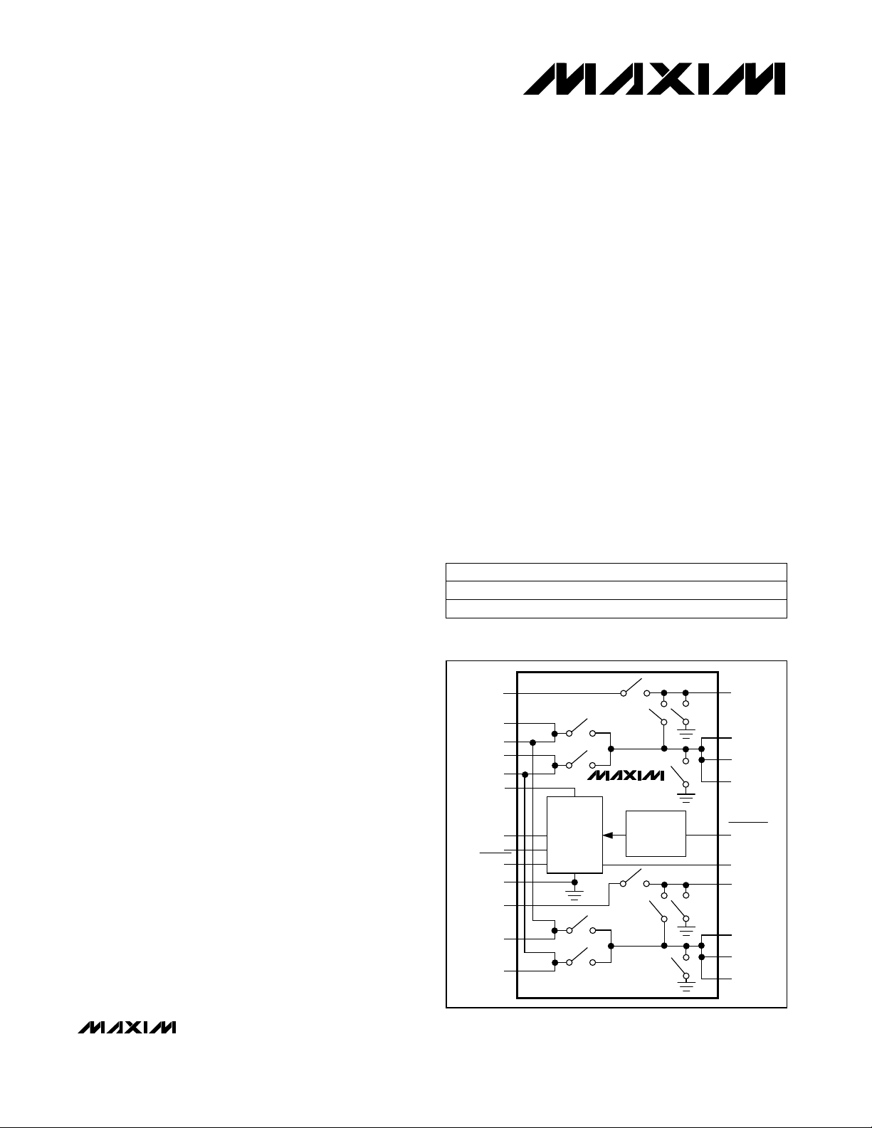
__________Simplified Block Diagram
12IN
SMBCLK
SMBDATA
SMBSUS
GND
12IN
VY
VY
VX
VX
VL
MAX1601/MAX1604
VDD
DECODE
LOGIC
ADDRESS
SELECT
OVERCURRENT
AND
THERMAL
SHUTDOWN
VPPA
VCCA
VCCA
VCCA
SMBALERT
ADR
VPPB
MAX1601/MAX1604
Pin Configuration appears on last page.
SMBus is a trademark of Intel Corp.
________________________________________________________________
VY
VX
Maxim Integrated Products
VCCB
VCCB
VCCB
1
For free samples & the latest literature: http://www.maxim-ic.com, or phone 1-800-998-8800
Dual-Channel CardBus and PCMCIA
Power Switches with SMBus™ Serial Interface
ABSOLUTE MAXIMUM RATINGS
Inputs/Outputs to GND
(VL, VX, VY, VCCA, VCCB) (Note 1)........................-0.3V, +6V
VPP Inputs/Outputs to GND
(12INA, 12INB, VPPA, VPPB) (Note 1)..................-0.3V, +15V
Inputs and Outputs to GND (SMBCLK, SMBDATA,
SMBSUS, SMBALERT) (Note 1)..............................-0.3V, +6V
ADR Input to GND ...........................................-0.3V, (VL + 0.3V)
VCCA, VCCB Output Current (Note 2).....................................4A
VPPA, VPPB Output Current (Note 2)...............................250mA
Note 1: There are no parasitic diodes between any of these pins, so there are no power-up sequencing restrictions (for example,
logic input signals can be applied even if all of the supply voltage inputs are grounded).
Note 2: VCC and VPP outputs are internally current-limited to safe values. See the
Stresses beyond those listed under “Absolute Maximum Ratings” may cause permanent damage to the device. These are stress ratings only, and functional
operation of the device at these or any other conditions beyond those indicated in the operational sections of the specifications is not implied. Exposure to
absolute maximum rating conditions for extended periods may affect device reliability.
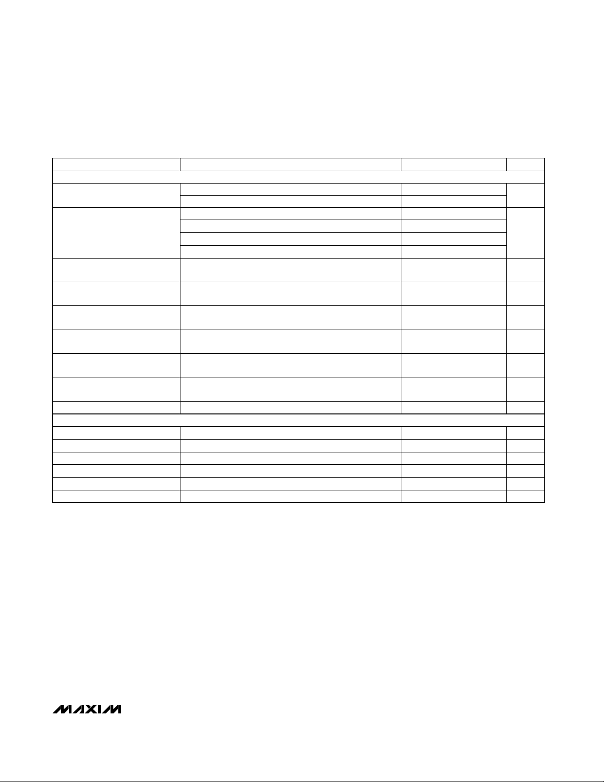
ELECTRICAL CHARACTERISTICS
MAX1601/MAX1604
(VL = VY = 3.3V, VX = 5V, 12INA = 12INB = 12V, TA= 0°C to +85°C, unless otherwise noted. Typical values are at TA= +25°C.)
CONDITIONS
POWER-SUPPLY SECTION
Input Voltage Range
Undervoltage Lockout Threshold
VCC SWITCHES
On-Resistance, VY Switches
VX, VY or VL
12INA, 12INB
VL falling edge
12IN falling edge
12IN rising edge
VX, VY falling edge
VX or VY, all switches 0V or high-Z,
control inputs = 0V or VL, TA= +25°C
Any combination of VY switches on,
control inputs = 0V or VL, no VCC loads
Any combination of VX switches on,
control inputs = 0V or high-Z, no VCC loads
12INA tied to 12INB, all switches 0V or high-Z,
control inputs = 0V or VL, TA= +25°C
12INA tied to 12INB, VPPA and VPPB 12V switches on,
control inputs = 0V or VL, no VPP loads
All switches 0V or high-Z, control inputs = 0V or VL,
TA= +25°C
Any combination of switches on
When using VL as shutdown pin (Note 3)
VCCA or VCCB, VX = VY = 3V to 5.5V
12INA = 12INB = 0V to 13V,
VY = 3V, VX = 0V to 5.5V,
I
12INA = 12INB = 0V to 13V, VX = 4.5V, VY = 0V to 5.5V,
I
SWITCH
SWITCH
= 1A, TA= +25°C
= 1A, TA= +25°C
VCCA, VCCB Short Circuit to GND............................Continuous
VPPA, VPPB Short Circuit to GND..............................Continuous
Continuous Power Dissipation (T
SSOP (derate 9.52mW/°C above +70°C) ....................762mW
Operating Temperature Range
MAX1601EAI/MAX1604EAI .............................-40°C to +85°C
Storage Temperature Range.............................-65°C to +160°C
Lead Temperature (soldering, 10sec).............................+300°C
Electrical Characteristics
MAX1601
MAX1604
= +70°C)
A
table.
3.0 5.5
11 13
2.4 2.5 2.8
1.8 3.0
5810
1.4 2.5 2.8
1 µA12IN_ Standby Supply Current
0.06 0.08
0.14 0.24
UNITSMIN TYP MAXPARAMETER
V
V
µA1Standby Supply Current
µA20 100VY Quiescent Supply Current
µA20 100VX Quiescent Supply Current
µA15 10012IN_ Quiescent Supply Current
µA410VL Standby Supply Current
µA25 150VL Quiescent Supply Current
V/µs0.05VL Fall Rate
A01Operating Output Current Range
Ω
Ω0.10 0.14On-Resistance, VX Switches
2 _______________________________________________________________________________________
Dual-Channel CardBus and PCMCIA
Power Switches with SMBus™ Serial Interface
ELECTRICAL CHARACTERISTICS (continued)
(VL = VY = 3.3V, VX = 5V, 12INA = 12INB = 12V, TA= 0°C to +85°C, unless otherwise noted. Typical values are at TA= +25°C.)
Output Propagation Delay
Plus Rise Time
Output Propagation Delay
Plus Fall Time
VPP SWITCHES
Output Propagation Delay
Plus Rise Time
Output Propagation Delay
Plus Fall Time
INTERFACE AND LOGIC SECTION
SMBALERT Signal Propagation
Delay
SMBALERT Output Low Voltage
SMBALERT Output Leakage Current
CONDITIONS
VCCA or VCCB A1.2 4.0Output Current Limit
VCCA or VCCB < 0.4V, programmed to 0V state mA20Output Sink Current
VCCA or VCCB forced to 0V, high-Z state,
TA= +25°C
VCCA or VCCB, 0V to VX or VY, CL= 30µF,
RL= 25Ω, 50% of input to 90% of output, TA= +25°C
VCCA or VCCB, 0V to VX or VY, CL= 1µF,
RL= open circuit, 10% to 90% points, TA= +25°C
VCCA or VCCB, VX or VY to 0V, CL= 30µF,
RL= open circuit, 50% of input to 10% of output,
TA= +25°C
VCCA or VCCB, VX or VY to 0V, CL= 1µF,
RL= 25Ω, 90% to 10% points
VPPA or VPPB
12IN = 11.6V, I
Programmed to VX (5V) or VY (3.3V), TA= +25°C
VPPA or VPPB, programmed to 12V
VPPA or VPPB < 0.4V, programmed to 0V state
VPPA or VPPB forced to 0V, high-Z state,
TA= +25°C
VPPA or VPPB, 0V to 12IN_, CL= 0.1µF,
50% of input to 90% of output, TA= +25°C
VPPA or VPPB, 0V to 12IN_, CL= 0.1µF,
10% to 90% points, TA= +25°C
VPPA or VPPB, 12IN_ to 0V, CL= 0.1µF,
50% of input to 10% of output, TA= +25°C
VPPA or VPPB, 12IN_ to 0V, CL= 0.1µF,
90% to 10% points
VCC_ or VPP_, load step to SMBALERT output,
50% point to 50% point (Note 3)
I
= 1mA, low state
SINK
V
SMBALERT
Hysteresis = +20°C (Note 4)
SMBSUS, SMBCLK, SMBDATA
SMBSUS, SMBCLK, SMBDATA
SMBDATA, I
= 5.5V, high state
SINK
= 100mA, TA= +25°C
SWITCH
= 4mA
100 800Output Rise Time
2.2
UNITSMIN TYP MAXPARAMETER
MAX1601/MAX1604
µA10Output Leakage Current
ms210
µs100 1200Output Rise Time
ms60 100
ms6Output Fall Time
mA0 120Operating Output Current Range
Ω0.70 1On-Resistance, 12V Switches
Ω13On-Resistance, VPP = VCC Switches
mA130 200 260Output Current Limit
mA10Output Sink Current
µA10Output Leakage Current
ms1.2 30
µs
ms960
ms1Output Fall Time
µs3
V0.4
µA-0.1 0.1
°C150Thermal Shutdown Threshold
V0.8Logic Input Low Voltage
VLogic Input High Voltage
V0.4Logic Output Low Voltage
_______________________________________________________________________________________ 3
Dual-Channel CardBus and PCMCIA
Power Switches with SMBus™ Serial Interface
ELECTRICAL CHARACTERISTICS (continued)
(VL = VY = 3.3V, VX = 5V, 12INA = 12INB = 12V, TA= 0°C to +85°C, unless otherwise noted. Typical values are at TA= +25°C.)
PARAMETER MIN TYP MAX UNITS
SMB Input Capacitance 5 pF
SMBCLK Clock Frequency DC 100 kHz
SMBCLK Clock Low Time 4.7 µs
SMBCLK Clock High Time 4 µst
SMB Repeated Start-Condition
Setup Time
SMB Start-Condition Hold Time 4 µs
SMB Stop-Condition Setup Time 4 µs
SMB Data Valid to SMBCLK RisingEdge Time
SMB Data Hold Time 0
Bus Free Time 4.7 µs
MAX1601/MAX1604
ADR Input Low Voltage 0.6 V
ADR Input High Voltage 1.5 V
Logic Input Bias Current -1 1 µA
SCL Fall to SDA Valid
(Master Clocking-In Data)
Start-Condition Setup
SMBSUS, SMBCLK, SMBDATA
SMBus spec = 10kHz min
t
10% to 10% points
LOW
90% to 90% points
HIGH
t
90% to 90% points
SU:STA
t
t
t
10% of SMBCLK
t
t
ADR, SMBSUS, SMBCLK, SMBDATA
10% of SMBDATA to 90% of SMBCLK
HD:STA
90% of SMBCLK to 10% of SMBDATA
SU:STO
10% or 90% of SMBDATA to
SU:DAT
(Note 5)
HD:DAT
between start and stop conditions
BUF
CONDITIONS
250 ns
500 ns
100 1000 ns
4.7 µs
ns
Note 3: Not production tested.
Note 4: Thermal limit not active in standby state (all switches programmed to GND or high-Z state).
Note 5: A transition must internally provide at least a hold time in order to bridge the undefined region (300ns max) of the falling
edge of SMBCLK.
4 _______________________________________________________________________________________
Dual-Channel CardBus and PCMCIA
Power Switches with SMBus™ Serial Interface
ELECTRICAL CHARACTERISTICS
(VL = VY = 3.3V, VX = 5V, 12INA = 12INB = 12V, TA= -40°C to +85°C, unless otherwise noted.)
CONDITIONS
POWER-SUPPLY SECTION
Input Voltage Range
Undervoltage Lockout Threshold
VX Quiescent Supply Current
INTERFACE AND LOGIC SECTION
SMBALERT Output Low Voltage
Logic Input High Voltage
Logic Output Low Voltage
ADR Input Low Voltage
ADR Input High Voltage
VX, VY or VL
12INA, 12INB
VL falling edge, hysteresis = 1%
12IN falling edge
12IN rising edge
VX, VY falling edge
VX or VY, all switches 0V or high-Z,
control inputs = 0V or VL
Any combination of VY switches on,
control inputs = 0V or VL, no VCC loads
Any combination of VX switches on,
control inputs = 0V or high-Z, no VCC loads
12INA tied to 12INB, all switches 0V or high-Z,
control inputs = 0V or VL
12INA tied to 12INB, VPPA and VPPB 12V switches on,
control inputs = 0V or VL, no VPP loads
All switches 0V or high-Z, control inputs = 0V or VL
Any combination of switches on
I
= 1mA, low state
SINK
SMBCLK, SMBDATA, SMBSUS
SMBCLK, SMBDATA, SMBSUS
SMBDATA, I
SINK
= 4mA
UNITSMIN TYP MAXPARAMETER
3.0 5.5
11 13
2.3 2.9
1.8
510
1.4 2.9
15
2.2
0.4
0.6
1.5
V
V
µA15Standby Supply Current
µA100VY Quiescent Supply Current
µA100
µA12IN_ Standby Supply Current
µA10012IN_ Quiescent Supply Current
µA15VL Standby Supply Current
µA150VL Quiescent Supply Current
V0.4
V0.8Logic Input Low Voltage
V
V
V
V
MAX1601/MAX1604
_______________________________________________________________________________________ 5

Dual-Channel CardBus and PCMCIA
Power Switches with SMBus™ Serial Interface
__________________________________________Typical Operating Characteristics
(VL = VY = 3.3V, VX = 5V, 12IN, TA = +25°C, unless otherwise noted.)
VCC_ SWITCHING (RISE)
6
4
VCC_
(V)
2
0
INPUT
(V)
5
0
200µs/div
CL = 30µF, RL = 25Ω
CONTROL
MAX1601/MAX1604
VCC_ SWITCHING (FALL)
6
4
VCC_
(V)
2
0
INPUT
(V)
5
0
CONTROL
MAX1601/4 TOC-01
MAX1601/4 TOC-03
VCC_
(V)
CONTROL
INPUT
(V)
VCC_
(V)
CONTROL
INPUT
(V)
3
2
1
0
5
0
CL = 1µF, RL = ∞
6
4
2
0
5
0
VCC_ SWITCHING (RISE)
MAX1601/4 TOC-02
500µs/div
VCC_ SWITCHING (FALL)
MAX1601/4 TOC-04
VPP_
(V)
CONTROL
INPUT
(V)
CL = 33µF, RL = ∞
15
10
5
0
5
0
CL = 0.1µF, RL = ∞
10ms/div
VPP_ SWITCHING (RISE)
200µs/div
MAX1601/4 TOC-05
VPP_
(V)
CONTROL
INPUT
(V)
CL = 1µF, RL = 25Ω
15
10
5
0
5
0
CL = 0.1µF, RL = ∞
VPP_ SWITCHING (FALL)
10ms/div
2ms/div
6 _______________________________________________________________________________________
MAX1601/4 TOC-06

Dual-Channel CardBus and PCMCIA
Power Switches with SMBus™ Serial Interface
_____________________________Typical Operating Characteristics (continued)
(VL = VY = 3.3V, VX = 5V, 12IN, TA = +25°C, unless otherwise noted.)
INPUT CURRENT (VCC OUTPUT SHORTED)
2.0
1.5
1.0
0.5
0
1ms/div
INPUT CURRENT (VPP OUTPUT SHORTED)
10
5
0
300
200
100
0
MAX1601/4 TOC-09
MAX1601/4 TOC-11
VCC_
(V)
VPP_
(V)
VCC_ CURRENT LIMITING
4
2
0
CL = 1µF, RESISTIVE OVERLOAD, RL = 1Ω
VPP_ CURRENT LIMITING
10
5
0
2ms/div
MAX1601/4 TOC-08
MAX1601/4 TOC-10
I
VY
(A)
VPP_
(V)
I
12IN_
(mA)
MAX1601/MAX1604
CL = 1µF, RL = 50Ω
2ms/div
RL = 0.1Ω
100µs/div
VCC_ SHUTDOWN RESPONSE
4
VL
(V)
VCC_
(V)
2
0
4
2
0
100µs/div
CIRCUIT OF FIGURE 2
MAX1601/4 TOC-12
_______________________________________________________________________________________
7

Dual-Channel CardBus and PCMCIA
Power Switches with SMBus™ Serial Interface
_____________________________Typical Operating Characteristics (continued)
(VL = VY = 3.3V, VX = 5V, 12IN, TA = +25°C, unless otherwise noted.)
VX ON-RESISTANCE
vs. VCC_ LOAD CURRENT
110
105
100
95
90
(mΩ)
85
ON
80
VX R
75
70
65
MAX1601/MAX1604
60
200
0 1000
400 600 800
VCC_ LOAD CURRENT (mA)
TA = +85°C
TA = +25°C
TA = -40°C
MAX1601/4 TOC-13
(mΩ)
ON
VY R
12IN_ ON-RESISTANCE vs. CURRENT
725
720
715
710
(mΩ)
ON
705
700
12IN R
695
690
685
20 40 60 80
0 100 120 140
CURRENT (mA)
VY ON-RESISTANCE vs. CURRENT
MAX1601
80
75
70
65
60
55
50
45
40
35
30
200 400 600 800
0 1000
CURRENT (mA)
TA = +85°C
TA = +25°C
TA = -40°C
12IN_ ON-RESISTANCE vs. TEMPERATURE
950
VPPA
VPPB
MAX1601/4 TOC-15
900
850
800
(mΩ)
ON
750
700
12IN R
650
600
550
-40 60 80 100
165
160
MAX1601/4 TOC-14
155
150
145
(mΩ)
140
ON
135
VY R
130
125
120
115
-20 0 20 40
TEMPERATURE (°C)
VY ON-RESISTANCE vs. CURRENT
MAX1604
TA = +85°C
TA = +25°C
TA = -40°C
0 1000
200 400 600 800
CURRENT (mA)
MAX1601/4 TOC-16
MAX1600/3 TOC-20
VX, VY SUPPLY CURRENT
vs. INPUT VOLTAGE
0.9
0.8
0.7
0.6
0.5
0.4
0.3
0.2
VX, VY SUPPLY CURRENT (µA)
0.1
0
1234
056
INPUT VOLTAGE (V)
VX
VY
MAX1601/4 TOC-17
12IN SUPPLY CURRENT (µA)
7
6
5
4
3
2
1
0
12IN SUPPLY CURRENT
vs. INPUT VOLTAGE
70
60
MAX1601/4 TOC-18
50
40
30
20
VL SUPPLY CURRENT (µA)
10
0
01012
2468
INPUT VOLTAGE (V)
056
VL SUPPLY CURRENT
vs. VL INPUT VOLTAGE
VX = VY = 0V
12IN
1234
INPUT VOLTAGE (V)
8 _______________________________________________________________________________________
NORMAL
OPERATION
SHUTDOWN
MAX1601/4 TOC-19

Dual-Channel CardBus and PCMCIA
Power Switches with SMBus™ Serial Interface
______________________________________________________________Pin Description
PIN
1, 25 GND Ground
2, 3,
26, 27
4 12INA +12V Supply Voltage Input, internally connects to channel A VPP switch. Tie to VPPA if not used.
5 VPPA Channel A VPP Output
6, 8, 10 VX
7, 22, 24 VCCA Channel A VCC Outputs
9, 18, 20 VCCB Channel B VCC Outputs
11 VPPB Channel B VPP Output
12 12INB +12V Supply Voltage Input, internally connects to channel B VPP switch. Tie to VPPB if not used.
13 ADR Address Input, sets SMBus address location. See Table 1 for address selection.
14
15 SMBCLK SMBus Clock Input
16 SMBDATA SMBus Data Input/Output, open drain
17
19, 21, 23 VY
28 VL
NAME FUNCTION
N.C. No internal connection
VX Supply-Voltage Inputs. VX pins must be connected together. Input range is 3V to 5.5V. VX is
normally connected to 5V.
SMBus Suspend-Mode Control Input. The device will execute commands previously stored in
SMBSUS
SMBALERT
the normal-mode register if SMBSUS is high, or will execute commands previously stored in the
suspend-mode register if SMBSUS is low.
Fault-Detection Interrupt Output. SMBALERT goes low if either channel VCC or VPP switch is
current limiting or undervoltage lockout, or if the thermal protection circuit is activated.
SMBALERT is an open-drain output that requires an external pull-up resistor.
VY Supply-Voltage Inputs. VY pins must be connected together. Input range is 3V to 5.5V. VY is
normally connected to 3V.
Logic Supply-Voltage Inputs. Connect to the +3.3V or +5V host system supply. VL can be supplied via the output of a CMOS-logic gate to produce an overriding shutdown. When used as a
shutdown input, VL should have a 1kΩ series resistor with a 0.1µF capacitor to ground (Figure 2).
Note that VL must be greater than undervoltage lockout for any switches to be turned on.
MAX1601/MAX1604
_______________________________________________________________________________________ 9

Dual-Channel CardBus and PCMCIA
Power Switches with SMBus™ Serial Interface
VB12
12IN
VY
MAX1601/MAX1604
VY
VX
VX
CHARGE
PUMP
VB3
CHARGE
PUMP
VB5
CHARGE
PUMP
0.08Ω
0.14Ω
*
CURRENT
LIMIT
CURRENT
LIMIT
CURRENT
LIMIT
1/2 MAX1601/MAX1604
3Ω
VPPA
40Ω
VCCA
VCCA
VCCA
20Ω
SMBCLK
SMBDATA
SMBSUS
ADR
SMB
VDD
VL
SHDN
THERMAL
SHUTDOWN
*0.24Ω FOR THE MAX1604
Figure 1. Functional Diagram (one channel of two)
10 ______________________________________________________________________________________
SMBALERT
GND

Dual-Channel CardBus and PCMCIA
Power Switches with SMBus™ Serial Interface
_______________Detailed Description
The MAX1601/MAX1604 power-switching ICs contain a
network of low-resistance MOSFET switches that deliver
selectable VCC and VPP voltages to two Cardbus or
PC Card host sockets. The MAX1601/MAX1604 differ
only in the VY switch on-resistance. Figure 1 is the
detailed block diagram.
The power-input pins (VY, VX, 12IN_) are completely
independent. Low inrush current is guaranteed by controlled switch rise times. VCC’s 100µs minimum output
rise time is 100% tested with a 1µF capacitive load, and
VPP’s 1ms minimum rise time is guaranteed with a 0.1µF
load. These respective capacitive loads are chosen as
worst-case card-insertion parameters. The internal
switching control allows VCC and VPP rise times to be
controlled, and makes them nearly independent of resistive and capacitive loads (see rise-time photos in the
Typical Operating Characteristics
function of loading, and are compensated by internal
circuitry.
Power savings is automatic: internal charge pumps draw
very low current when the VCC switches are static.
Standby mode reduces switch supply current to 1µA.
Driving the VL pin low with an external logic gate (master
shutdown) reduces total supply current to1µA (Figure 2).
The MAX1601/MAX1604 have three operating modes:
normal, standby, and shutdown. Normal mode supplies
the selected outputs with their appropriate supply voltages. Standby mode places all switches at ground, high
impedance, or a combination of the two. Shutdown mode
turns all switches off, and puts the VCC and VPP outputs
into a high-impedance state. Pull VL low to enter shutdown
mode. To ensure a 0.05V/µs fall rate on VL, use a 1kΩ
series resistor and a 0.1µF capacitor to ground (Figure 2).
Overcurrent Protection
Peak detecting circuitry protects both the VCC and
VPP switches against overcurrent conditions. When
current through any switch exceeds the internal current
limit (4A for VCC switches and 200mA for VPP switches), the switch turns off briefly, then turns on again at
the controlled rise rate. If the overcurrent condition
lasts more than 2µs, the SMBALERT output latches
). Fall times are a
Operating Modes
3.3V
VY
MAX1601
MAX1604
VPPA
VCCA
TO
SOCKETS
A AND B
VPPB
VCCB
MASTER
SHUTDOWN
74HC04
Figure 2. Master Shutdown Circuit
1k
0.1µF
VL
low. A continuous short-circuit condition results in a
pulsed output current until thermal shutdown is
reached. SMBALERT is open-drain and requires an
external pull-up resistor.
Thermal Shutdown
If the IC junction temperature rises above +150°C, the
thermal shutdown circuitry opens all switches, including
the GND switches, and SMBALERT is pulled low. When
the temperature falls below +130°C, the switches turn
on again at the controlled rise rate. If the overcurrent
condition remains, the part cycles between thermal
shutdown and overcurrent.
Undervoltage Lockout
If the VX or VY switch input voltage drops below 1.5V,
the associated switch turns off and SMBALERT goes
low. For example, if VY is 3.3V and VX is 0V, and if the
interface controller selects VY, the VCCA output will be
3.3V. If VX is selected, VCCA changes to a high-impedance output and SMBALERT goes low.
When a voltage is initially applied to 12IN_, it must be
greater than 8V to allow the switch to operate.
Operation continues until the voltage falls below 2V (the
VPP output is high impedance).
When VL drops to less than 2.3V, all switches are
turned off and the VCC and VPP outputs are high
impedance.
MAX1601/MAX1604
______________________________________________________________________________________ 11

Dual-Channel CardBus and PCMCIA
Power Switches with SMBus™ Serial Interface
______SMBus™ Interface Operation
The SMBus serial interface is a two-wire interface with
multi-mastering capability, intended to control lowspeed peripheral devices in low-power portable equipment applications. SMBus is similar to I2C™ and
AccessBus, but has slightly different logic threshold
voltage levels, different fixed addresses, and a suspend-mode register capability. To obtain a complete
set of specifications on the SMBus interface, call Intel at
(800) 253-3696 and ask for product code SBS5220.
SMBus Addressing
These dual-channel PC Card switch devices respond to
two of four different addresses, depending on the state
of the ADR address pin. Normal writing to the device is
done by transmitting one of four addresses, followed by
a single data byte, to program the channel selected.
Write transmissions to the interrupt pointer address are
not supported by these devices. Reading from the
MAX1601/MAX1604
device is done by transmitting one of two addresses cor-
Table 1. SMBus Addressing
SMB
ADDRESS
0001100 Don’t care N/A Interrupt Pointer
1010000 Grounded Channel A Channel A/B faults
1010001 Grounded Channel B Channel A/B faults
1010010 Tied to VL Channel A Channel A/B faults
1010011 Tied to VL Channel B Channel A/B faults
ADR PIN
WRITE
FUNCTION
READ FUNCTION
responding to either the A channel address (which will
provide data about faults for both A and B channels) or
to the interrupt pointer address (discussed later).
The normal start condition consists of a high-to-low
transition on SMBDATA while SMBCLK is high. The
7-bit address is followed by a bit that designates a read
or write operation: high = read, low = write. If the 7-bit
address matches one of the supported function
addresses, the IC issues an acknowledge pulse by
pulling the SMBDATA line low. If the address is not
valid, the IC stays off of the bus and ignores any data
on the bus until a new start condition is detected. Once
the IC receives a valid address that includes a write bit,
it expects to receive one additional byte of data. If a
stop condition or new start condition is detected before
a complete byte of data is clocked in, the IC interprets
this as an error and all of the data is rejected and lost.
SMBDATA and SMBCLK are Schmitt triggered and can
accommodate slower edges. However, rising edges
should still be faster than 1µs, and falling edges should
be faster than 300ns.
SMBus Write Operations
If the IC receives a valid address immediately followed
by a write bit, the IC becomes a slave receiver. The
slave IC generates a first acknowledge after the
address and write bit, and a second acknowledge after
the command byte. A stop condition following the command (data) byte causes immediate execution of the
command, unless the data included a low SUS/OP bit.
If the data included a low SUS/OP bit, the command is
stored in the suspend-mode register and is executed
only when the SMBSUS pin is pulled low (Figure 3).
Table 2. Command Format for Channel A Write Operations (address 1010000 or 1010010)
FUNCTIONPOR STATENAMEBIT
0OP/SUS7 (MSB)
I2C is a trademark of Philips Corp.
SMBus is a trademark of Intel Corp.
12 ______________________________________________________________________________________
Operate/suspend bit. Selects which latch receives data: high = operation,
low = suspend.
Turns on VCCA when high, pulls VCCA to GND when low.0VCCAON6
If VCCA is on, a high connects VY to VCCA, and a low connects VX to VCCA.0VCCA3/55
Puts VCCA in a high-impedance state when high. Overrides VCCAON.0VCCAHIZ4
Turns on VPPA when high, pulls VPPA to GND when low.0VPPAON3
If VPPA is on, a high connects VPPA to 12INA, and a low connects VPPA to VCCA.0VPPAPGM2
Puts VPPA in a high-impedance state when high. Overrides VPPAON.0VPPAHIZ1
Masks fault interrupts from both channel A and channel B when high.0MASKFLT0 (LSB)

Dual-Channel CardBus and PCMCIA
Power Switches with SMBus™ Serial Interface
Table 3. Command Format for Channel B Write Operations (address 1010001 or 1010011)
BIT NAME POR STATE FUNCTION
7 (MSB) OP/SUS 0
6 VCCBON 0 Turns on VCCB when high, pulls VCCB to GND when low.
5 VCCB3/5 0 If VCCB is on, a high connects VY to VCCB, and a low connects VX to VCCB.
4 VCCBHIZ 0 Puts VCCB in a high-impedance state when high. Overrides VCCBON.
3 VPPBON 0 Turns on VPPB when high, pulls VPPB to GND when low.
2 VPPBPGM 0 If VPPB is on, a high connects VPPB to 12INB, and a low connects VPPB to VCCB.
1 VPPBHIZ 0 Puts VPPB in a high-impedance state when high. Overrides VPPBON.
0 (LSB) RFU 0 Reserved for future use.
Operate/suspend bit. Selects which latch receives data: high = operation,
low = suspend.
Table 4. Read Format for Interrupt Pointer Address (0001100)
BIT NAME POR STATE FUNCTION
7 (MSB) ADD7 0
6 ADD6 0
5 ADD5 0
4 ADD4 0
3 ADD3 0
2 ADD2 0
1 ADD1 0
0 (LSB) ADD0 0
ADD7 to ADD1 provide a return address for any interrupt query. For these devices, the
return addresses are:
1010000 = Channel A, ADD = low
1010001 = Channel B, ADD = low
1010010 = Channel A, ADD = high
1010011 = Channel B, ADD = high
MAX1601/MAX1604
Table 5. Read Format for Power Switch Address (1010000 or 1010010)
BIT NAME POR STATE FUNCTION
7 (MSB) CATFAULT 0 Indicates catastrophic (thermal or undervoltage lockout) fault when high.
6 FAULT1 0 Indicates VCCA overcurrent/undervoltage lockout when high.
5 FAULT2 0 Indicates VPPA overcurrent/undervoltage lockout when high.
4 FAULT3 0 Indicates VCCB overcurrent/undervoltage lockout when high.
3 FAULT4 0 Indicates VPPB overcurrent/undervoltage lockout when high.
2 SIG/DUAL 0 Indicates dual part (single-channel devices would read 1).
1 RFU 0 Reserved for future use.
0 (LSB) RFU 0 Reserved for future use.
______________________________________________________________________________________ 13
LATCHED?
Y
Y
Y
Y
Y
N
N
N

Dual-Channel CardBus and PCMCIA
Power Switches with SMBus™ Serial Interface
AB CD
t
LOWtHIGH
SMBCLK
SMBDATA
t
t
HD:STA
SU:STA
A = START CONDITION
B = MSB OF ADDRESS CLOCKED INTO SLAVE
C = LSB OF ADDRESS CLOCKED INTO SLAVE
D = R/W BIT CLOCKED INTO SLAVE
E = SLAVE PULLS SMBDATA LINE LOW
t
SU:DAT
F = ACKNOWLEDGE BIT CLOCKED INTO MASTER
G = MSB OF DATA CLOCKED INTO SLAVE (OP/SUS BIT)
H = LSB OF DATA CLOCKED INTO SLAVE
I = SLAVE PULLS SMBDATA LINE LOW
MAX1601/MAX1604
Figure 3. SMBus Write Timing Diagram
SMBus Read Operations
If the IC receives a valid address that includes a read
bit, the IC becomes a slave transmitter. After receiving
the address data, the IC generates an acknowledge
during the acknowledge clock pulse and drives the
SMBDATA line in sync with SMBCLK. The SMB protocol requires that the master end the read transmission
by not acknowledging during the acknowledge bit of
SMBCLK. These PC Card ICs support the repeated
start-condition method for changing data-transfer direction; that is, a write transmission followed by a repeated
start instead of a stop condition prepares the IC for
data reading (Figure 4).
SMBus Interrupts
These PC Card power-switch ICs are slave devices
only, and never initiate communications except by
asserting an interrupt (by pulling SMBALERT low).
Interrupts are generated only for reporting fault conditions, including overcurrent at VCCA, VCCB, VPPA, or
VPPB, undervoltage lockout, and IC thermal overload. If
an interrupt occurs, it can be an indication of impending system failure. The host system can react by going
into suspend mode or taking other action. It can come
back later to interrogate the IC via the interrupt pointer
to determine status or perform corrective action (such
as disabling the appropriate power switch that might
be connected to a shorted PC card). The fastest
method for turning off the switches in response to a
E
FG H
t
HD:DAT
I
J
J = ACKNOWLEDGE CLOCKED INTO MASTER
K = ACKNOWLEDGE CLOCK PULSE
L = STOP CONDITION, DATA EXECUTED BY SLAVE
M = NEW START CONDITION
K
t
SU:STO
fault condition is to cycle the voltage on VL in order to
generate a power-on reset (which clears all of the
SMBus registers). Note that the SMBus registers retain
their data even if the main VX/VY supplies are turned
off, provided that VL remains powered.
When a fault occurs, SMBALERT is immediately asserted and latched low. If the fault is momentary and disappears before the IC is serviced, the data is still latched
in the interrupt pointer and SMBALERT remains asserted. Normally, the master (host system or PCMCIA digital controller) now sends out the interrupt pointer
address (00011000) followed by a read bit. SMBALERT
is cleared and the PC Card IC responds by putting out
its address on the bus. If the fault persists, SMBALERT
is re-asserted, but the data in the fault registers is not
reloaded. The data in the fault latches only reflects the
first time SMBALERT is asserted.
When the part enters operating mode, a false interrupt
flag may be issued. The user needs to send the interrupt address to clear the false interrupt.
Normally, the master sends out the appropriate PC Card
switch address on the bus, followed by a read bit. The
data in the fault registers is then clocked out onto the
bus (which also clears the fault registers). If the fault
persists, the fault bits and SMBALERT are latched
again.
M
L
t
BUF
14 ______________________________________________________________________________________

Dual-Channel CardBus and PCMCIA
Power Switches with SMBus™ Serial Interface
SMBCLK
SMBDATA
AB CD
t
t
HIGH
LOW
FG H
E
I
J
MAX1601/MAX1604
K
t
SU:STAtHD:STA
A = START CONDITION
B = MSB OF ADDRESS CLOCKED INTO SLAVE
C = LSB OF ADDRESS CLOCKED INTO SLAVE
D = R/W BIT CLOCKED INTO SLAVE
Figure 4. SMBus Read Timing Diagram
t
SU:DAT
E = SLAVE PULLS SMBDATA LINE LOW
F = ACKNOWLEDGE BIT CLOCKED INTO MASTER
G = MSB OF DATA CLOCKED INTO MASTER
H = LSB OF DATA CLOCKED INTO MASTER
The interrupt pointer address provides quick fault identification for simple slave devices that lack the complex,
expensive logic needed to be a bus master. The host
can read the interrupt pointer to determine which slave
device generated an SMBALERT interrupt signal. The
interrupt pointer address can activate several different
slave devices simultaneously, similar to an I2C general
call. Any slave device that generated an interrupt
attempts to identify itself by putting its own address on
the bus during the first read byte. If more than one slave
attempts to respond, bus arbitration rules apply and the
device with the lower address code wins. The losing
device won’t generate an acknowledge and will continue to hold the SMBALERT line low until serviced, which
implies that the host interrupt input must be level
sensitive.
__________Applications Information
t
t
SU:STO
BUF
I = ACKNOWLEDGE CLOCK PULSE
J = STOP CONDITION
K = NEW START CONDITION
Changing SMBCLK and SMBDATA
Simultaneously
When clocking data into the MAX1601/MAX1604, SMBDATA must not fall before SMBCLK. Otherwise, the
MAX1601/MAX1604 may interpret this as a start condition. Even when SMBDATA and SMBCLK fall at the
same instant, different fall times for the two signals may
cause the erroneous generation of a start condition. To
ensure that SMBDATA transitions after the falling edge of
SMBCLK, add an RC network to SBMDATA (Figure 6).
1k
VL
0.1µF
VX+5V
MAX1601
MAX1604
Supply Bypassing
Bypass the VY, VX, and 12IN_ inputs with ceramic 0.1µF
capacitors. Bypass the VCC_ and VPP_ outputs with a
0.1µF capacitor for noise reduction and ESD protection.
Power-Up
Apply power to the VL input before any of the switch
inputs. If VX, VY, or 12IN receive power before VL rises
above 2.8V, the supply current may be artificially high
(about 5mA). When the voltage on VL is greater than
2.8V (operating mode), the part consumes its specified
24µA. To avoid power sequencing, diode-OR VX and
VY to VL through a 1kΩ resistor (Figure 5). Take care
not to allow VL to drop below the 2.8V maximum undervoltage lockout threshold.
______________________________________________________________________________________ 15
VY
Figure 5. Powering from Either VX or VY
+5V
CIRRUS LOGIC
CL-PD6730
SMBDATA
SMBCLK
Figure 6. Application with Cirrus Logic Interface
10k
PULL-UP
1.5k
100pF
SMBDATA
MAX1601
MAX1604
SMBCLK

Dual-Channel CardBus and PCMCIA
Power Switches with SMBus™ Serial Interface
__________________Pin Configuration ___________________Chip Information
TOP VIEW
GND
1
N.C.
2
N.C.
3
12INA
4
VPPA
5
VX
VCCA
VX
VCCB
VX
VPPB
MAX1601/MAX1604
12INB
ADR
SMBSUS
MAX1601
6
MAX1604
7
8
9
10
11
12
13
14
28
27
26
25
24
23
22
21
20
19
18
17
16
15
VL
N.C.
N.C.
GND
VCCA
VY
VCCA
VY
VCCB
VY
VCCB
SMBALERT
SMBDATA
SMBCLK
TRANSISTOR COUNT: 4372
SSOP
________________________________________________________Package Information
DIM
A
A1
B
C
α
HE
C
L
D
E
e
H
L
α
INCHES
MIN
0.068
0.002
0.010
0.004
0.205
0.301
0.025
MAX
0.078
0.008
0.015
0.008
SEE VARIATIONS
0.209
0.311
0.037
0˚
8˚
MILLIMETERS
MIN
1.73
0.05
0.25
0.09
5.20
0.65 BSC0.0256 BSC
7.65
0.63
0˚
MAX
1.99
0.21
0.38
0.20
5.38
7.90
0.95
8˚
14
16
20
24
28
INCHES
MIN
0.239
0.239
0.278
0.317
0.397
DIM
PINS
e
SSOP
A
SHRINK
SMALL-OUTLINE
B
A1
PACKAGE
D
D
D
D
D
MAX
0.249
0.249
0.289
0.328
0.407
MILLIMETERS
MAX
MIN
6.33
6.07
6.33
6.07
7.33
7.07
8.33
8.07
10.33
10.07
21-0056A
D
Maxim cannot assume responsibility for use of any circuitry other than circuitry entirely embodied in a Maxim product. No circuit patent licenses are
Maxim cannot assume responsibility for use of any circuitry other than circuitry entirely embodied in a Maxim product. No circuit patent licenses are
Maxim cannot assume responsibility for use of any circuitry other than circuitry entirely embodied in a Maxim product. No circuit patent licenses are
Maxim cannot assume responsibility for use of any circuitry other than circuitry entirely embodied in a Maxim product. No circuit patent licenses are
Maxim cannot assume responsibility for use of any circuitry other than circuitry entirely embodied in a Maxim product. No circuit patent licenses are
Maxim cannot assume responsibility for use of any circuitry other than circuitry entirely embodied in a Maxim product. No circuit patent licenses are
implied. Maxim reserves the right to change the circuitry and specifications without notice at any time.
implied. Maxim reserves the right to change the circuitry and specifications without notice at any time.
implied. Maxim reserves the right to change the circuitry and specifications without notice at any time.
implied. Maxim reserves the right to change the circuitry and specifications without notice at any time.
implied. Maxim reserves the right to change the circuitry and specifications without notice at any time.
implied. Maxim reserves the right to change the circuitry and specifications without notice at any time.
16
__________________Maxim Integrated Products, 120 San Gabriel Drive, Sunnyvale, CA 94086 (408) 737-7600
16
__________________Maxim Integrated Products, 120 San Gabriel Drive, Sunnyvale, CA 94086 (408) 737-7600
16
__________________Maxim Integrated Products, 120 San Gabriel Drive, Sunnyvale, CA 94086 (408) 737-7600
16
__________________Maxim Integrated Products, 120 San Gabriel Drive, Sunnyvale, CA 94086 (408) 737-7600
16
__________________Maxim Integrated Products, 120 San Gabriel Drive, Sunnyvale, CA 94086 (408) 737-7600
16
__________________Maxim Integrated Products, 120 San Gabriel Drive, Sunnyvale, CA 94086 (408) 737-7600
© 1996 Maxim Integrated Products Printed USA is a registered trademark of Maxim Integrated Products.
© 1996 Maxim Integrated Products Printed USA is a registered trademark of Maxim Integrated Products.
© 1996 Maxim Integrated Products Printed USA is a registered trademark of Maxim Integrated Products.
© 1996 Maxim Integrated Products Printed USA is a registered trademark of Maxim Integrated Products.
© 1996 Maxim Integrated Products Printed USA is a registered trademark of Maxim Integrated Products.
© 1996 Maxim Integrated Products Printed USA is a registered trademark of Maxim Integrated Products.
 Loading...